Authored by Jonathan Young on November 9, 2015
Email: youngj1ATunlv.nevada.edu
Project Description:
This project focuses on the knowledge learned in class and during lab to build an 8-bit up/down counter, as well as modifications to standard gates such as the NAND, NOR, and the inverter. This project will make heavy use of CMOS (NMOS and PMOS) devices to implement the above circuits and gates. The final result of this project is to take these circuits and fabricate them using the C5 process on an integrated circuit (IC) chip, which will be shipped to MOSIS for fabrication.
This report will detail the creation of each circuit chip, including schematics (using CMOS devices), symbols, layout (how chip will be produced using the C5 process), as well as design
verification via the use of simulations to verify overall design is functional. After the circuits are sent to MOSIS for fabrication and returned, they will each be verified for functionality with all variations being listed in this report. This will allow one to see the design tolerances of how the chips perform in computer aided simulations versus real world simulations.
Project Directions:
First half of the project (no layout, just schematics and symbols), of your design and an html report detailing operation (including simulations), is due at the beginning of lab on Nov. 9. Ensure that you have schematics with simulations for all of the cells listed below. Your up/down counter, for example, should be simulated showing, counting up, down, or both, resetting then counting, etc. Put your report (proj.htm) in a folder called /proj in your directory at CMOSedu. Dr. Baker will go over your designs with you, including running simulations, when lab meets on Nov. 9.
Second half of the project, a verified layout and documentation (in html), is due at the beginning of lab on Nov. 23. Again, I will meet with you on Nov. 23 to go over your layout and, again, put your report in the /proj folder in your directory at CMOSedu. Ensure that there is a link on your project report webpage to your zipped design directory. Finishing the projects by Nov. 23 will give us time to assemble chips for fabrication through MOSIS.
*Design of an 8-bit resettable (input "clear") up/down counter.
*The outputs of your counter should be buffered before connecting to a pad.
*A 31-stage ring oscillator with a buffer for driving a 20 pF off-chip load.
*NAND and NOR gates using 6/0.6 NMOSs and PMOSs
*An inverter made with a 6/0.6 NMOS and a 12/0.6 PMOS.
*Transistors, both PMOS and NMOS, measuring 6u/0.6u where all 4 terminals of each device are connected to bond pads (7 pads + common gnd pad). Note that only one pad is need for the common gnd pad. This pad is used to ground the p-substrate and provide ground to each test circuit.
*Using the 25k resistor laid out below and a 10k resistor implement a voltage divider (need only 1 more pad above the ones used for the 25k resistor).
*A 25k resistor implemented using the n-well (connect between 2 pads but we also need a common gnd pad).
Buffer Gate:
A buffer gate is commonly used to allow a circuit to drive a load that the original circuit is not capable of supplying due to a weak signal. This gate allows it to be placed in series with the original circuit's output to provide a full load (supply) or sinking capabilities depending on the output load, resistance, being placed on the output of the circuit. As per the requirements for this project, the ring oscillator design is required to drive a 20pF capacitive load on its output, which is connected to a pad (output terminal of an IC).
To achieve this requirement, a chain of inverters, with varying sizes, can be used, as each logic gate acts as an amplification source to the output signal provided from the supplying circuit.
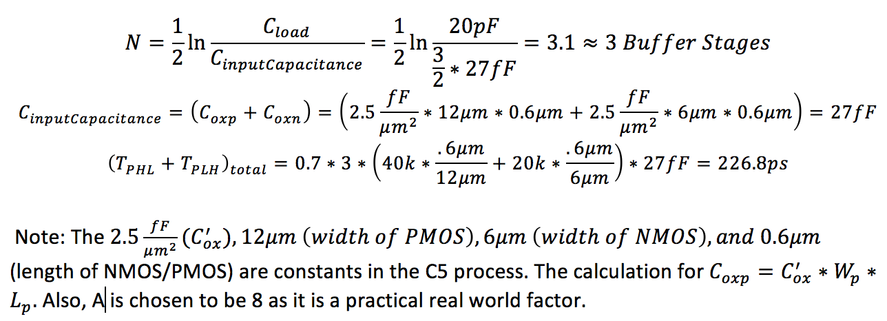
The question now becomes how many stages of inverters is needed. According to CMOS Circuit Design, Layout, and Simulation, Third Edition by R. Jacob Backer (Chapter 11), the number of inverter stages needed to create a buffer can be derived using the following formula:
What this means is that there will be three different stages of inverters connected in series. After each stage (set of inverters), the A (8) will be used to multiply the MOSFET's length and width and thus increase in size. The dimensions of this are seen below:
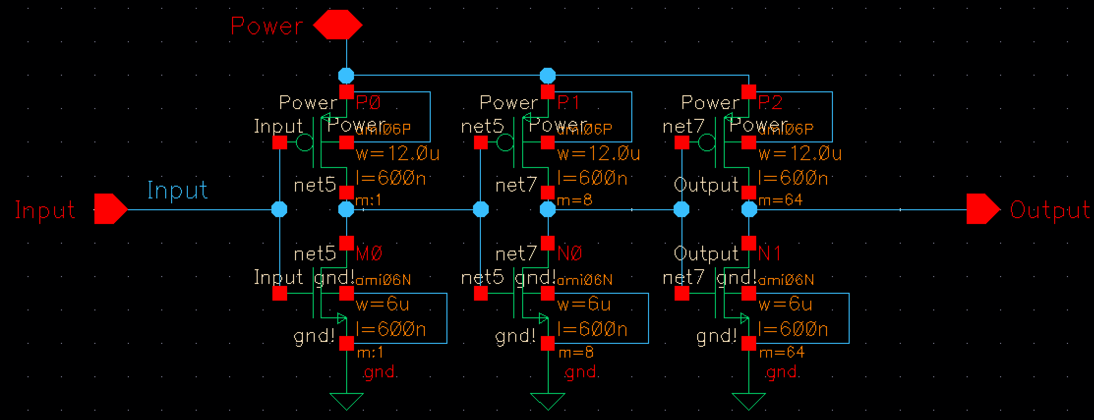
Figure 1:
This is the schematic of three stages of inverters, derived above with each input and output being connected in serial.
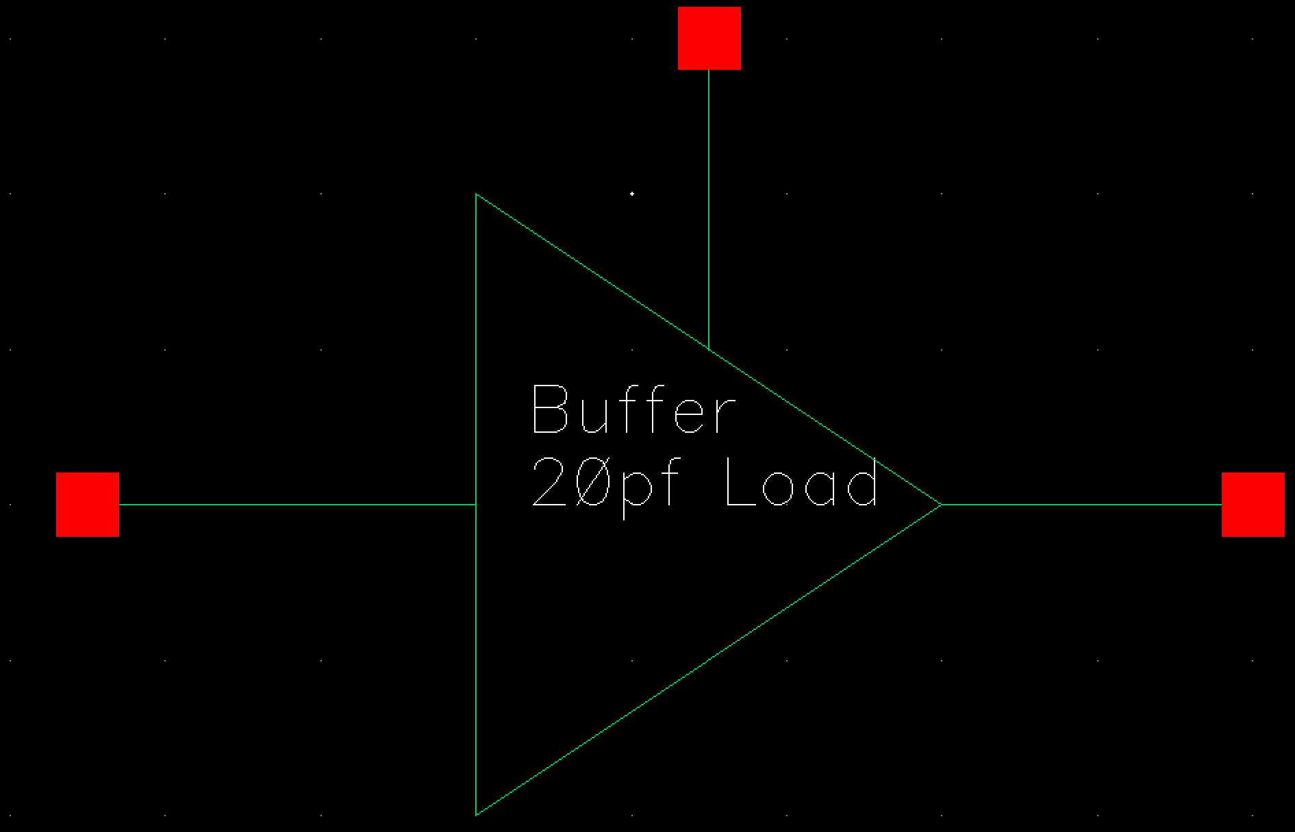
Figure 2:
This is the symbol that was created, which will reference the chain of inverters in figure 1.
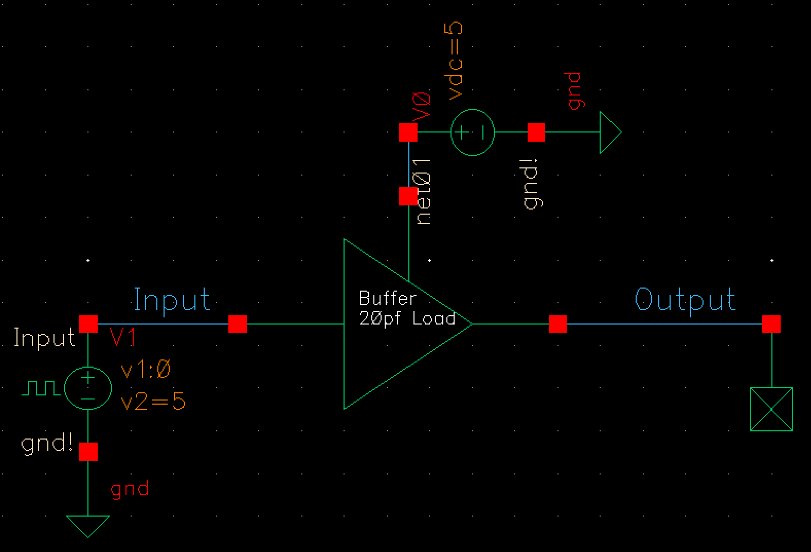
Figure 3:
This is the simulation schematic, where the symbol is instantiated and everything is connected to produce simulation waveforms to verify functionality of the buffer.
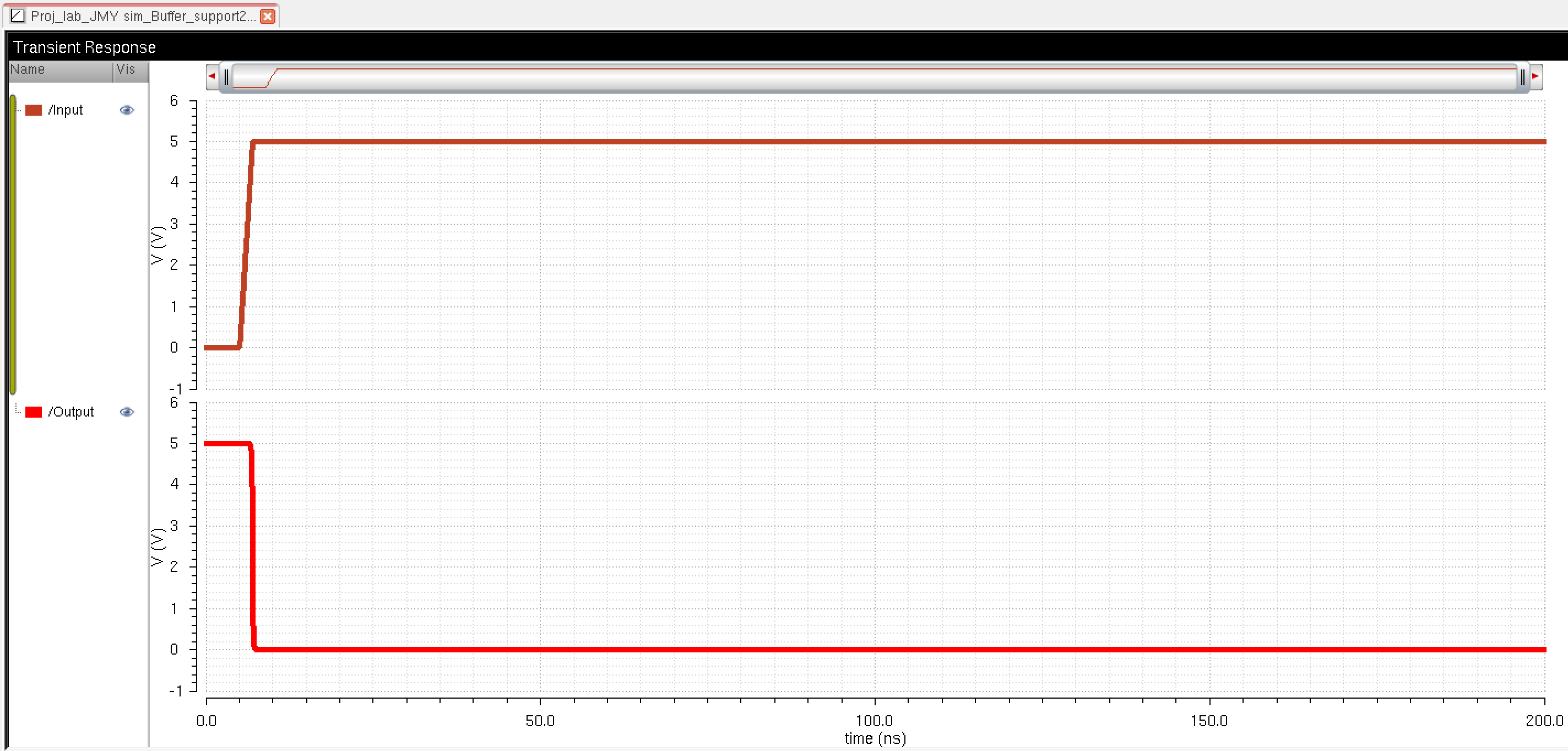
Figure 4:
This is the simulation, which resulted from the schematic in Figure 3. Notice however, the input has a small delay and that the output is more well defined. The purpose of a buffer not only allows the output to drive a larger load, but acts to sharpen a signal and give it a more well defined shape.
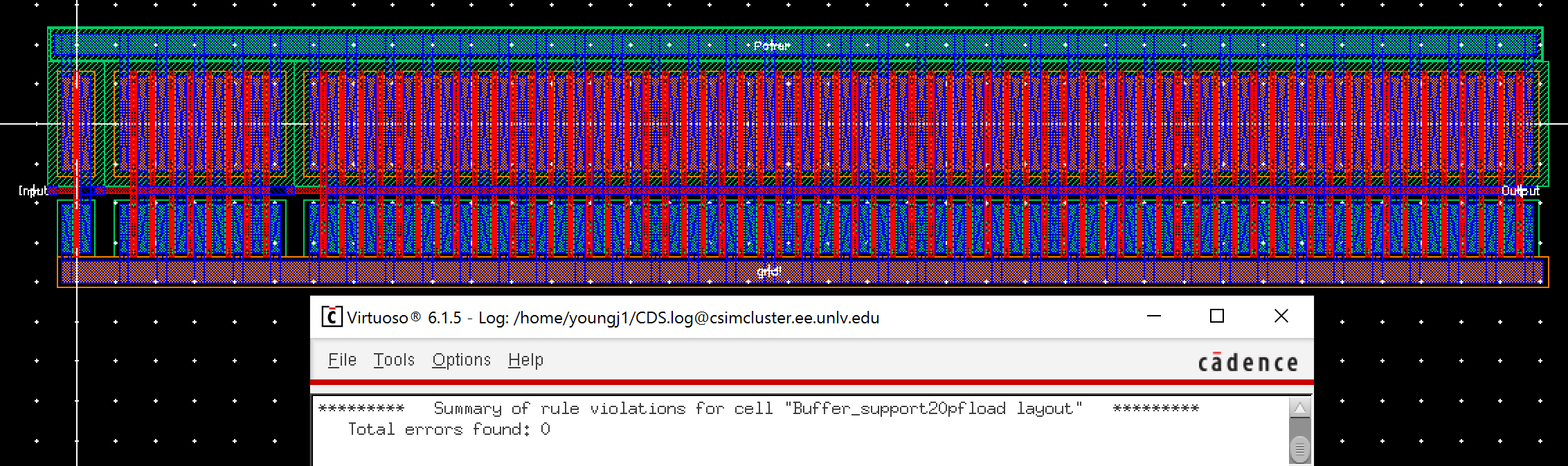
Layout 1:
This image is the layout of the buffer with three stages. It also shows that the layout DRCed without errors.
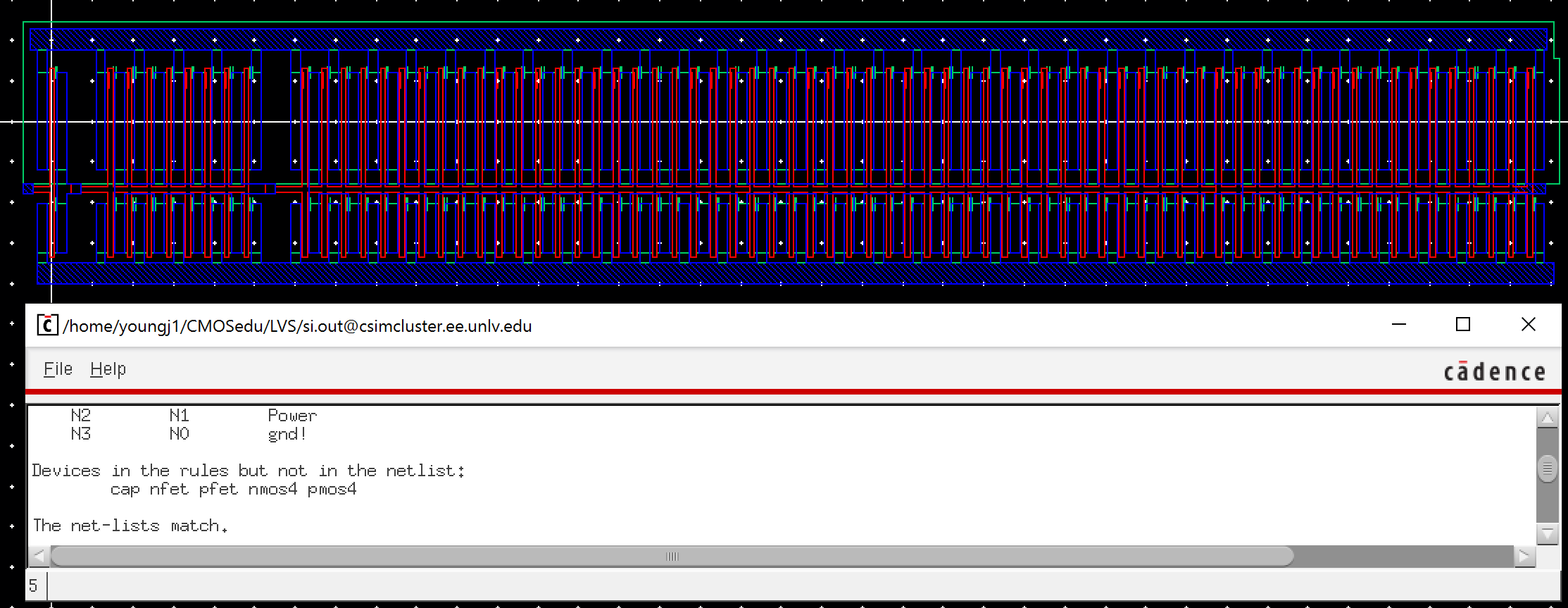
Layout 2:
This is the extracted layout of the buffer seen in Layout 1. It shows that LVS performed without errors.
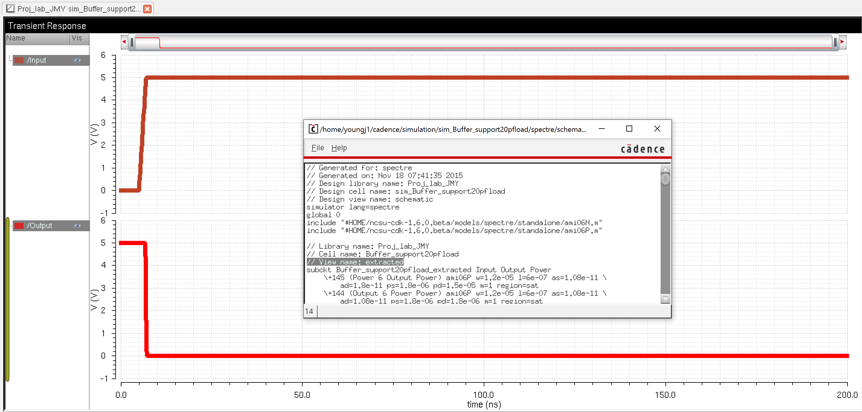
Layout 3:
This is an extracted simulation result using the layout of the circuit in Layout 2 to compare to the simulation of the schematic in Figure 4.
D Flip-Flop:
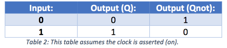
The D (data) flip-flop(FF) is known to store data (a single bit) and only change on the active edge of an input clock. The D flip-flop will output a Q, which is the output of the memory contents of the flip-flop that are stored. Qnot is the inverse of the Q output. If the clock leading into the D flip-flop is always high, then Q will mirror the input line (D), otherwise Q will display what is stored.
The following is a truth table for the D FF:
Figure 5:
This is the schematic of a D flip-flop which is constructed with inverters and transmission gates that utilize CMOS devices. For how the inverter and transmission gates are constructed, look at the respective sections below.
Figure 6:
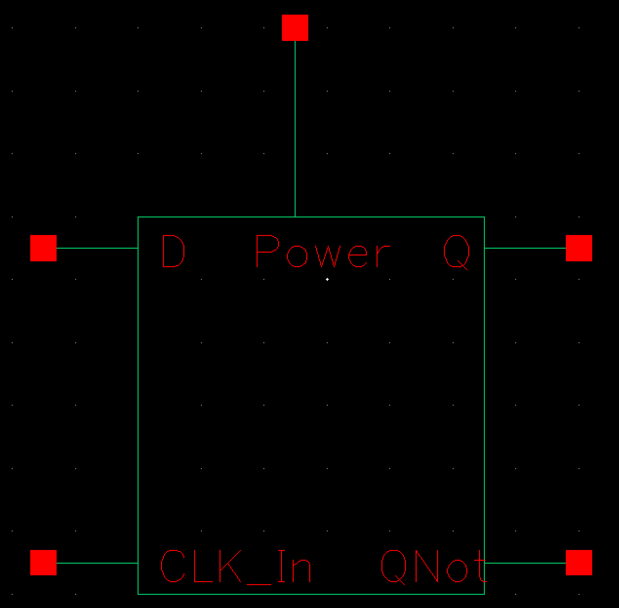
This is the symbol for the D flip-flop, which will be used for schematic instantiations.
Figure 7:
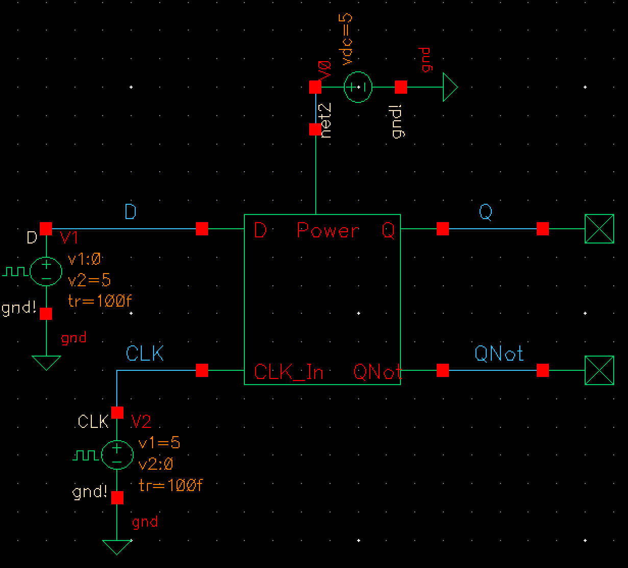
This is the simulation schematic, used to verify device functionality. Note: VDD is set to 5 volts which is used for the CMOS devices.
Figure 8:
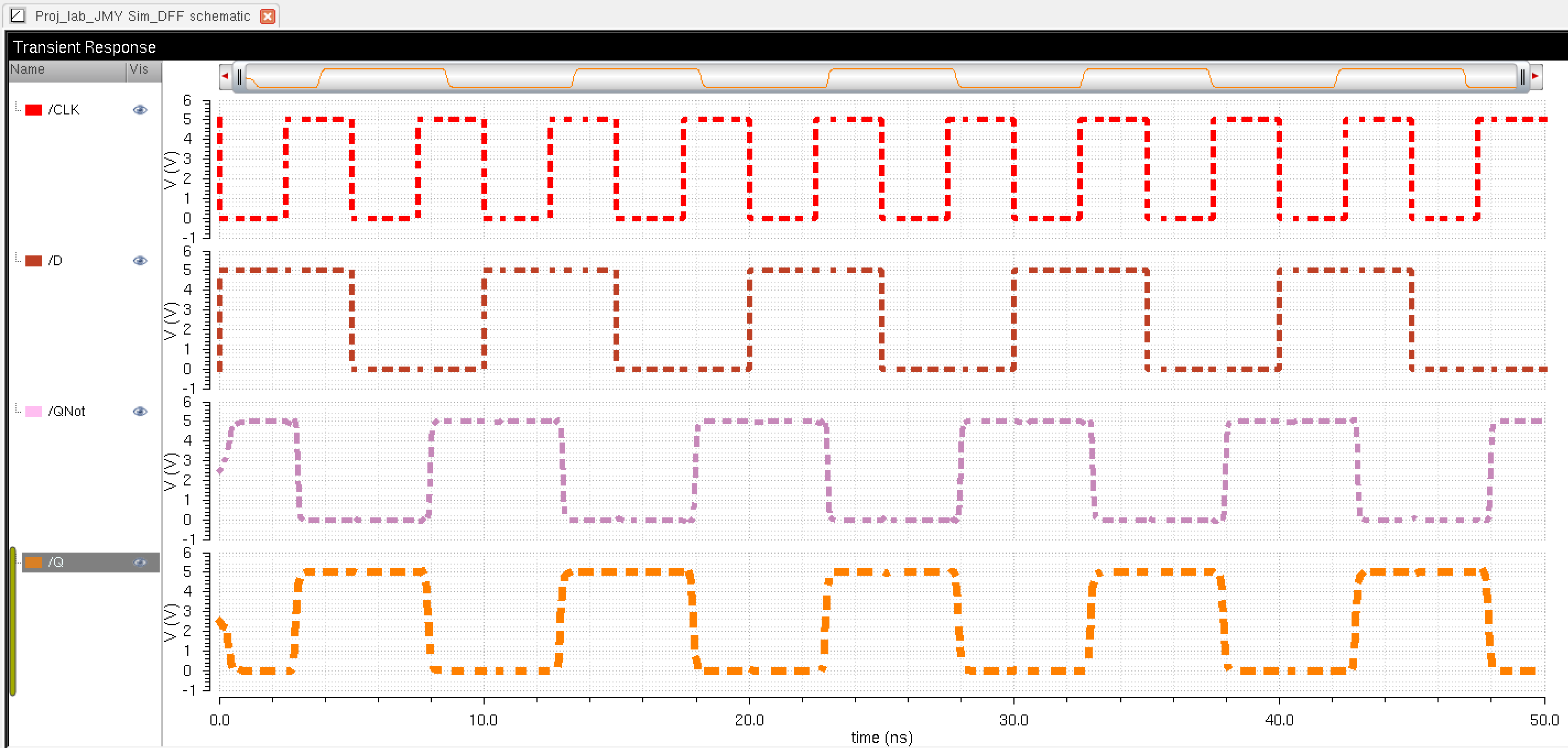
This is the simulation of the D FF, which is a result of the of the simulation schematic seen in Figure 7. Note: How QNot is the opposite (inverse) of Q, thus this shows correct functionality at the active clock edge which mirrors the input D.
D Flip-Flop with Clear:
The D FF with clear is the same design as the D FF described above, with the only minor change being the addition of the clear. This is implemented using NAND gates to allow the signal to propagate through or be blocked based on the clear signal being asserted or de-asserted. Note: The design here is for an active high clear and that it is asynchronous (allowing all logic gates to be reset regardless of the transition state it its presently in).
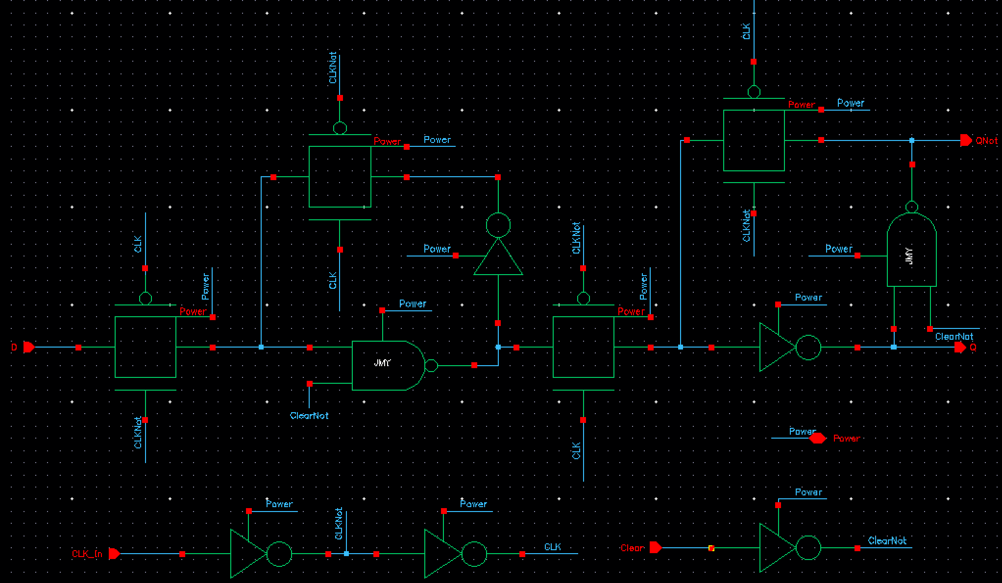
Figure 9:
This is the schematic for a D FF with a clear. Note: It is similar to figure 5, with two inverters being changed to NAND gates to allow the asynchronous clear to function.
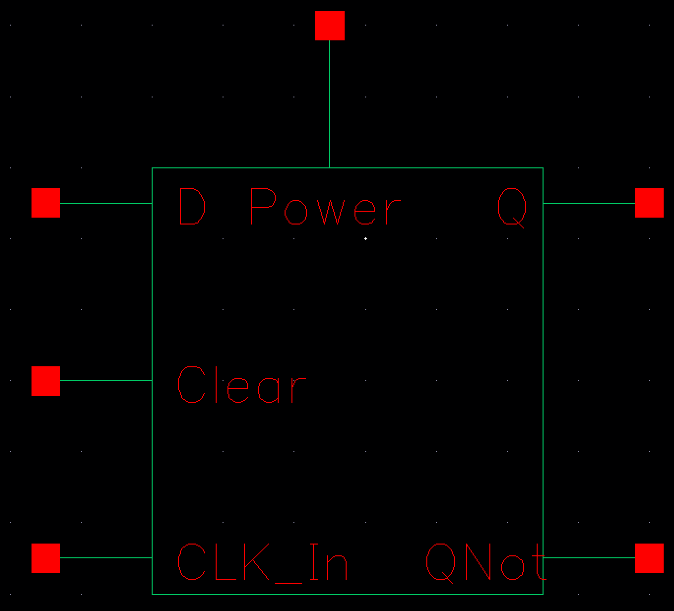
Figure 10:
This is the symbol for the D FF with clear.
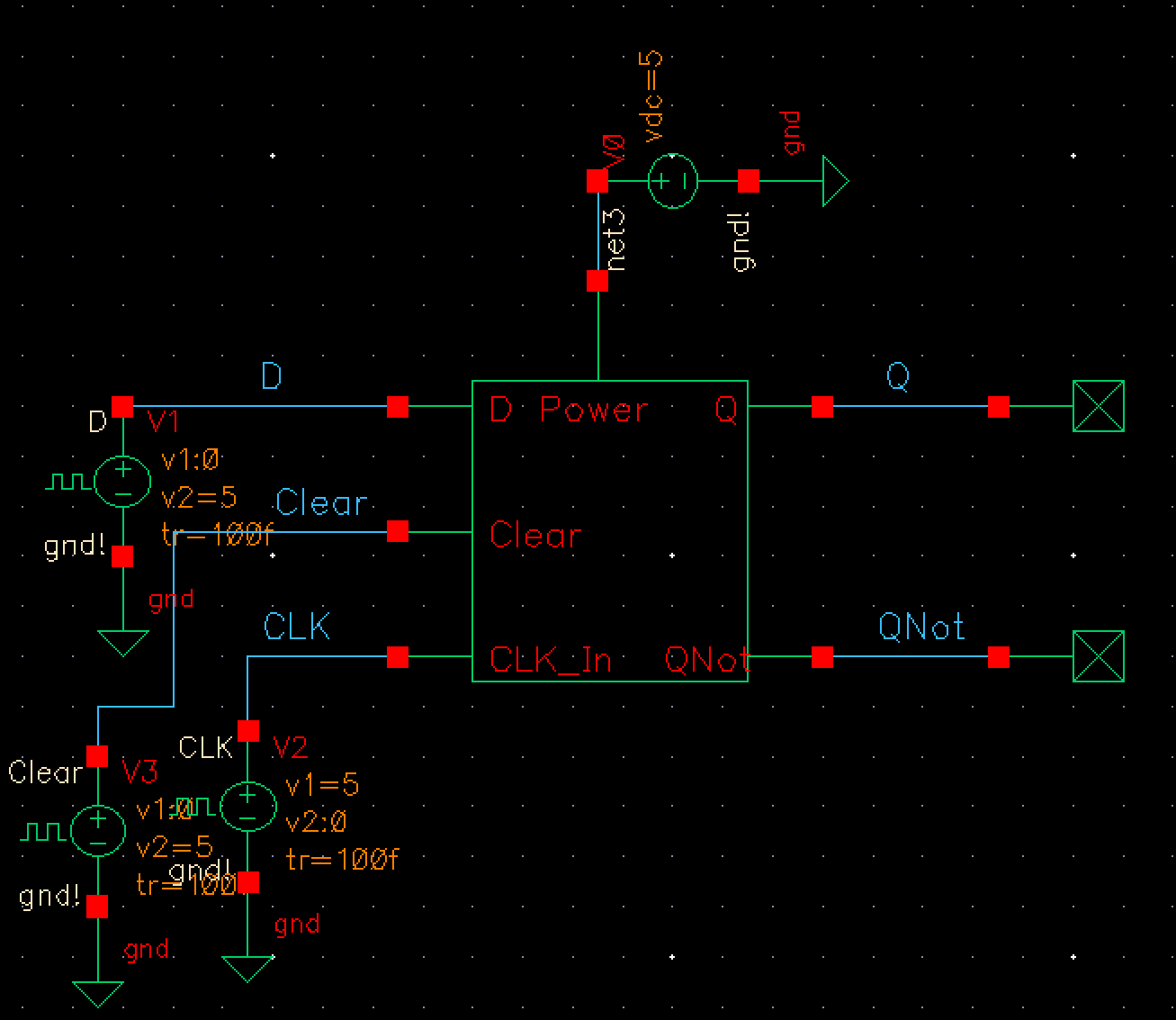
Figure 11:
This is the simulation schematic, used to test the functionality of the D FF with clear to ensure it produces the desired results.
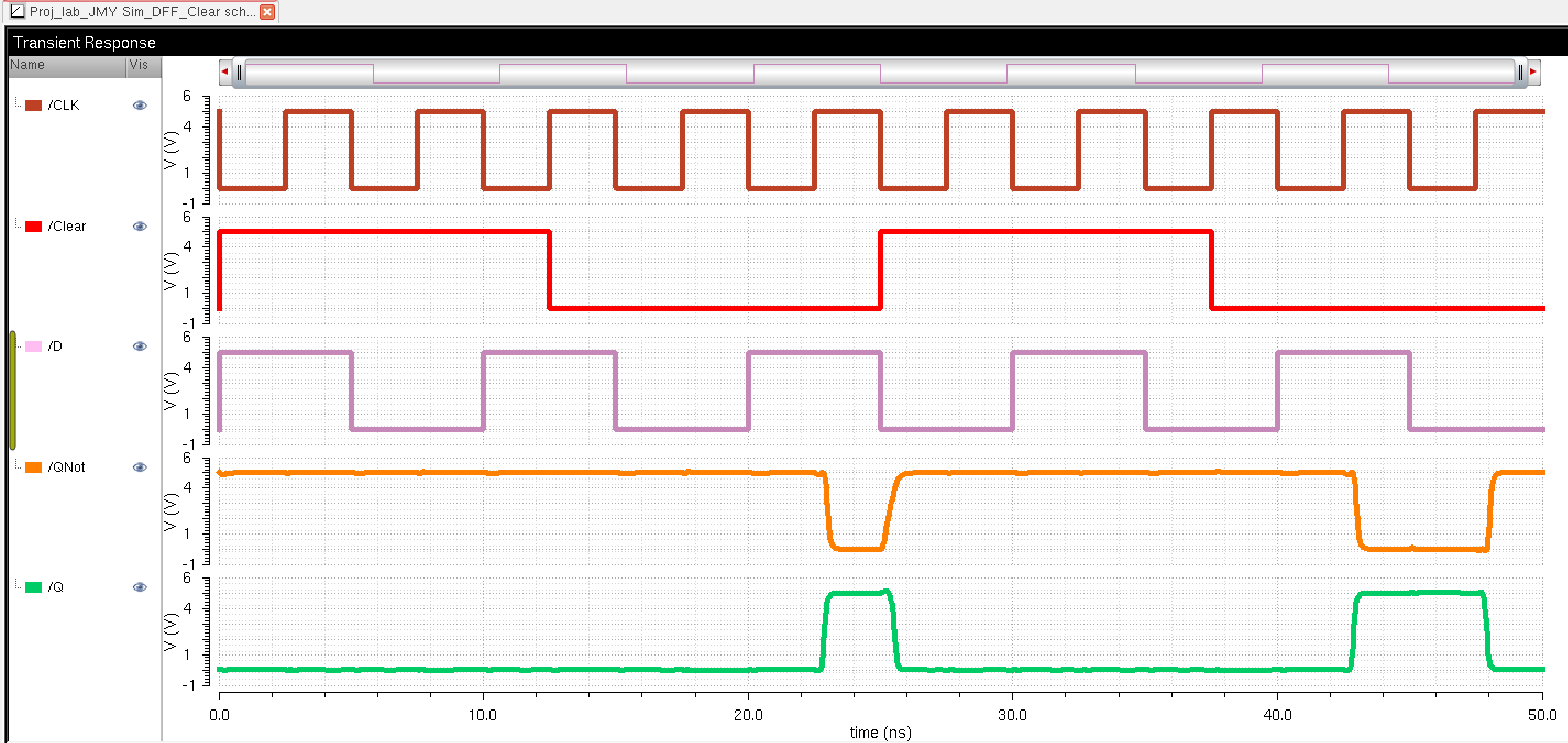
Figure 12:
This is the simulation produced from figure 11, which shows the functionality of the active high clear. Note: The functionality of the D FF is seen in figure 8.
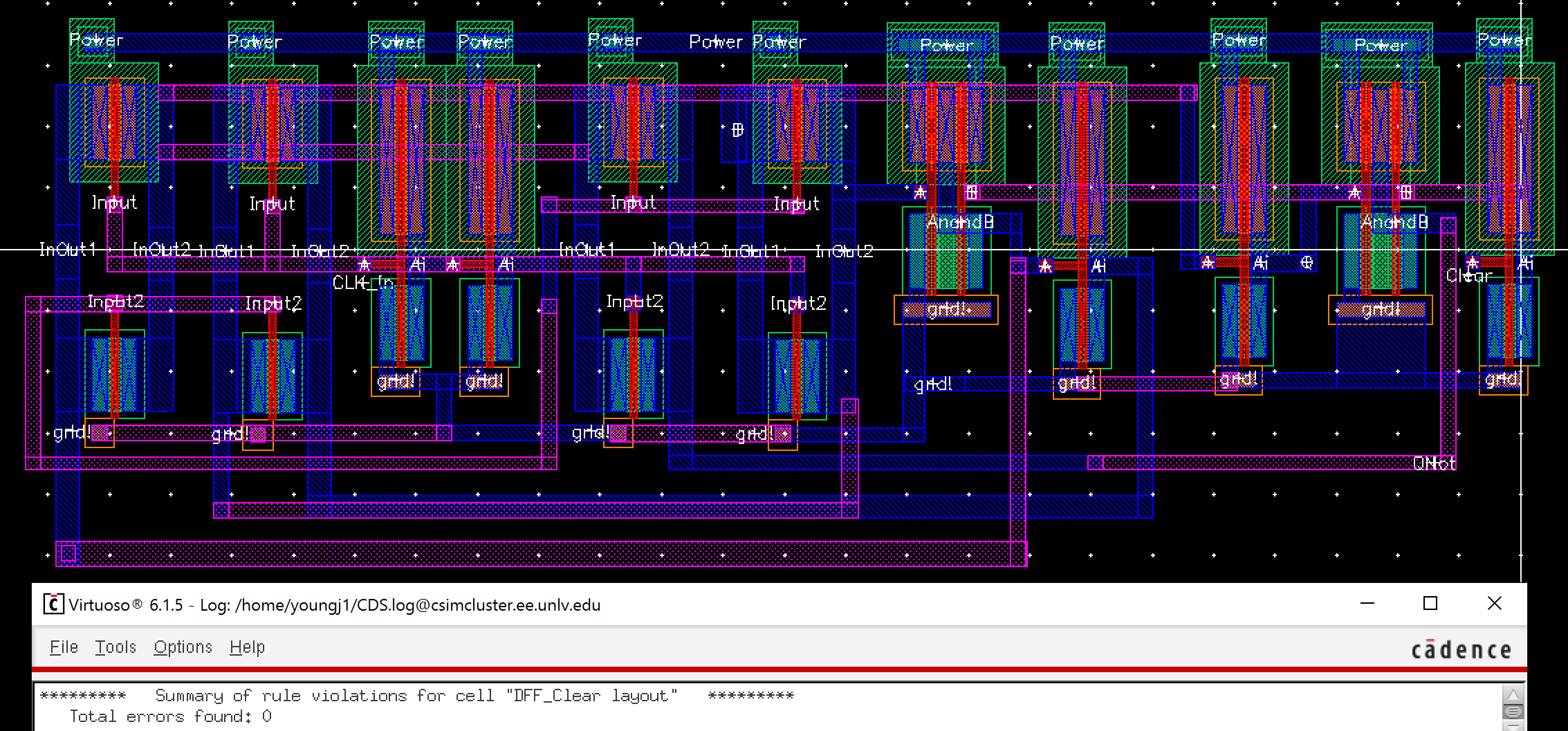
Layout 4:
This is the layout of the D FF with a clear. Note: The D FF without a clear will be nearly identical, with the NAND gates replaced with inverters as detailed above. As this circuit was required for the counter, it was the only one laid out. Once can see that it passes DRC without errors and has appropriate labels.
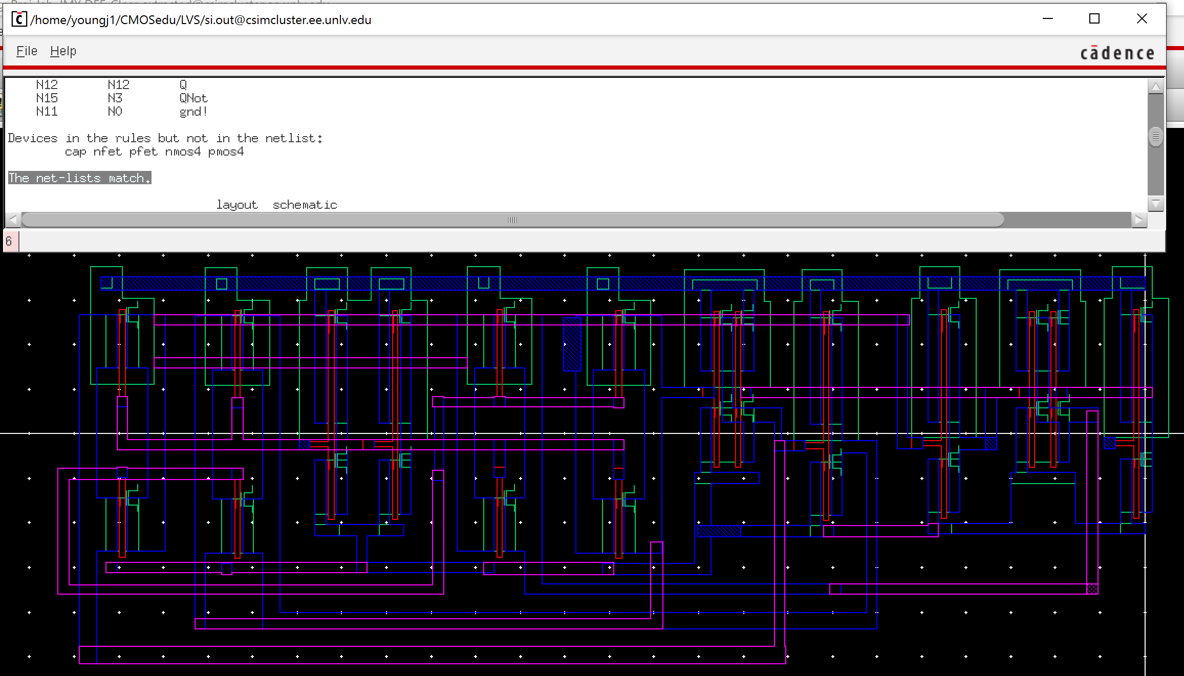
Layout 5:
This is the extracted layout, seen in Layout 4. It passes LVS without errors.
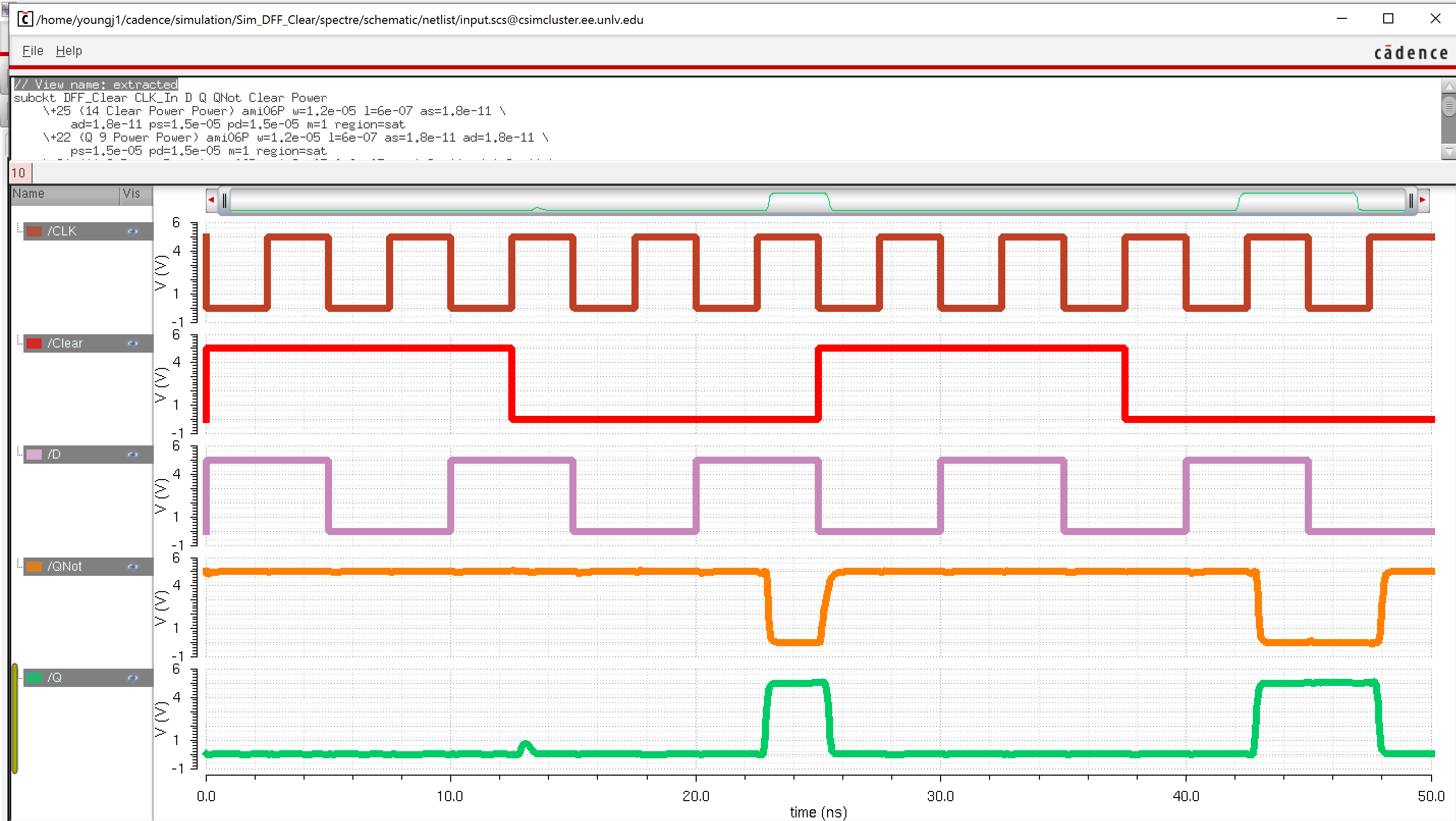
Layout 6:
This is an extracted simulation result using the layout of the circuit in Layout 5 to compare to the simulation of the schematic in Figure 12. Note: The little bumps in the Q and Qnot signals, which shows noise on the output line.
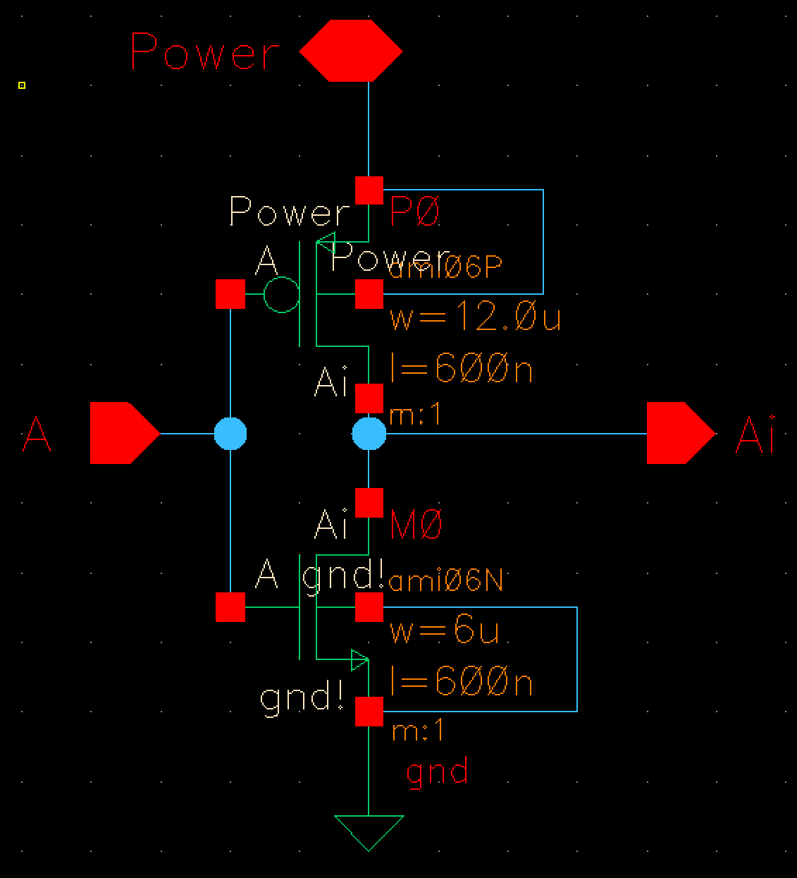
Inverter
The inverter is designed with both a PMOS and NMOS, which allows an input signal to be inverted. For example, if the input is high the NMOS will activate and allow the output signal to travel to ground. As the PMOS is off only a signal of 0 (low) is passed to the drain of the NMOS, since both are connected the output signal is tied directly to ground and thus the output is 0. Thus an inverter will produce the opposite output of its input. If the input is high, the output is low or vice versa.
Note: This inverter design is what is used in the buffer and for all other schematics which require the use of an inverter.
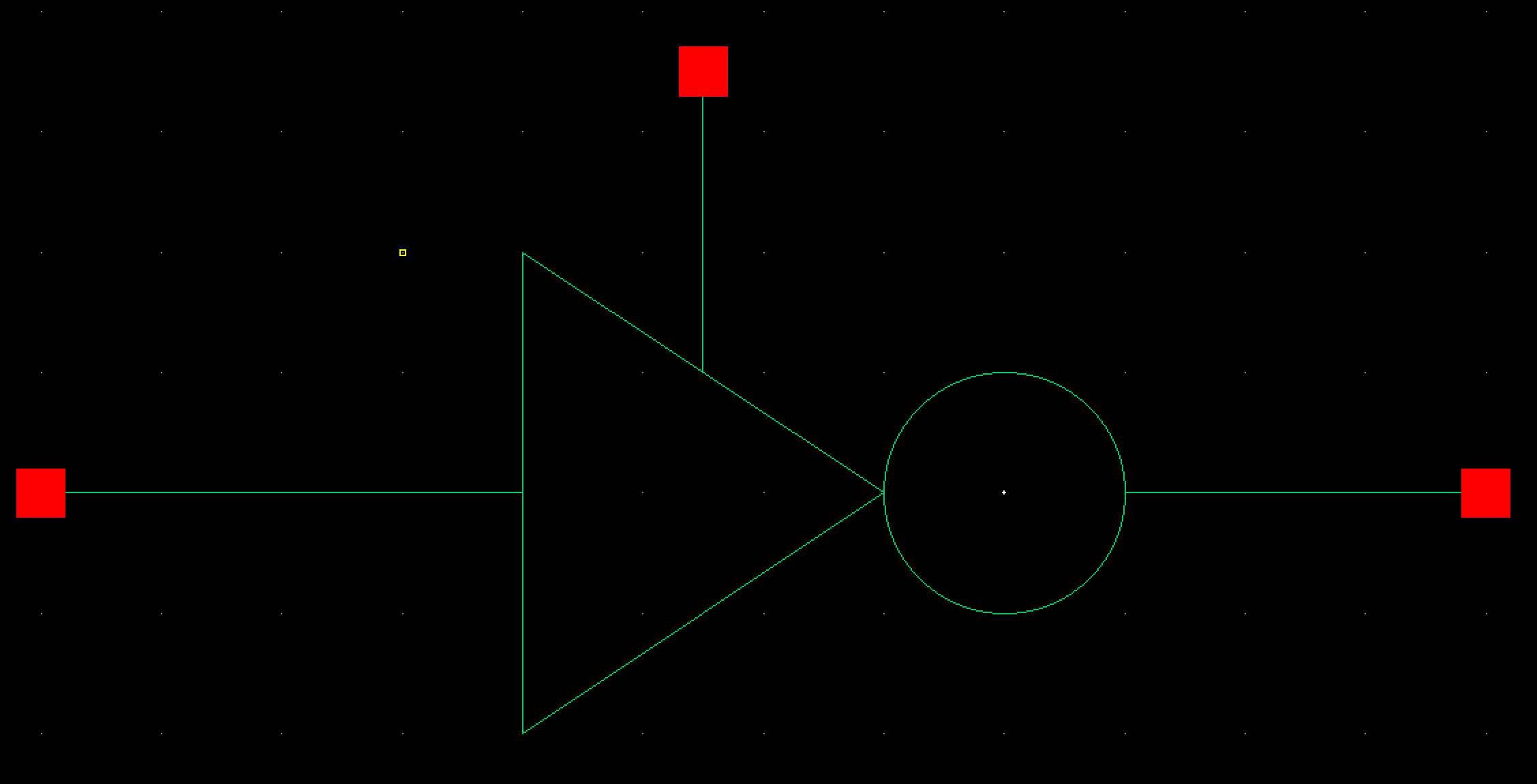
Figure 13:
This is the schematic for an inverter, using CMOS devices.
Figure 14:
This is a symbol for the inverter.
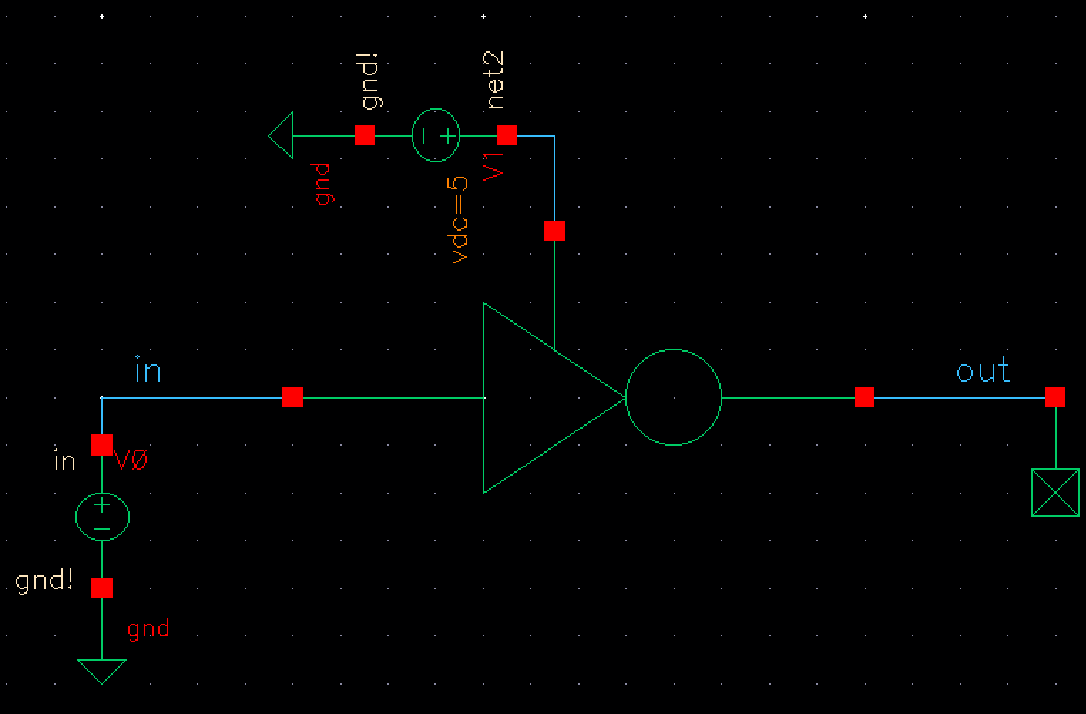
Figure 15:
This is the simulation schematic for the inverter to see if the circuit performs as it should.
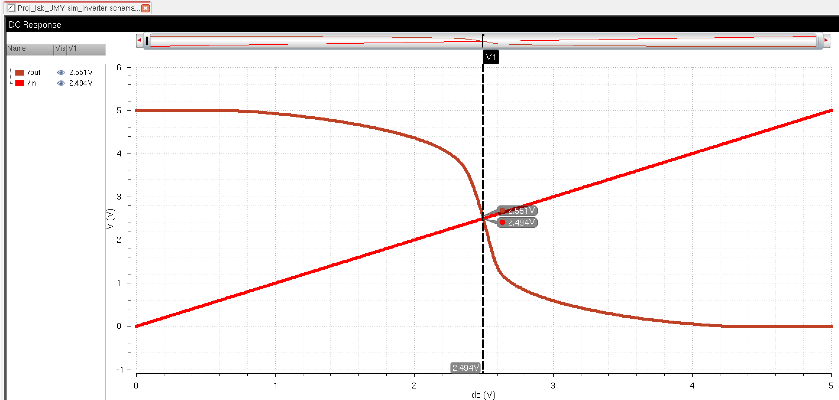
Figure 16:
The simulation schematic in figure 15 produces this transfer curves simulation showing the operation of the inverter.
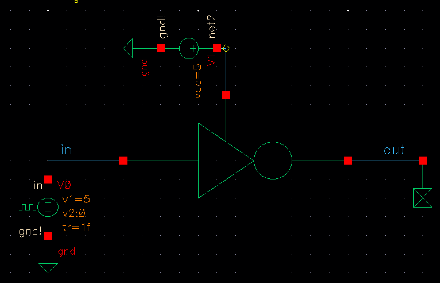
Figure 17:
This is a simulation schematic, which will be used to perform a functionality test using transient analysis.
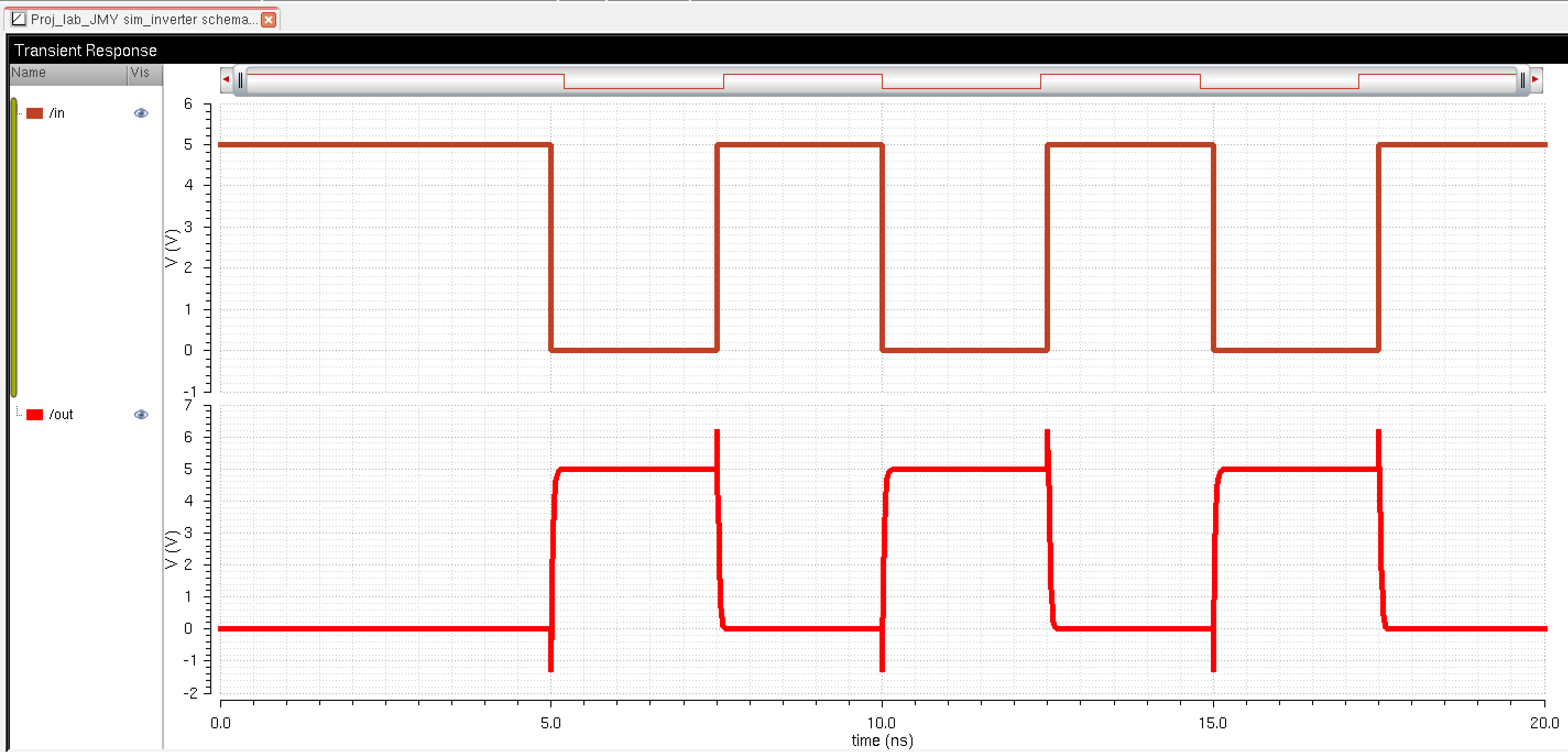
Figure 18:
This is the simulation produced from figure 17, showing the input and output stages of the inverter. Note: They are opposite of each other and thus have the correct functionality.
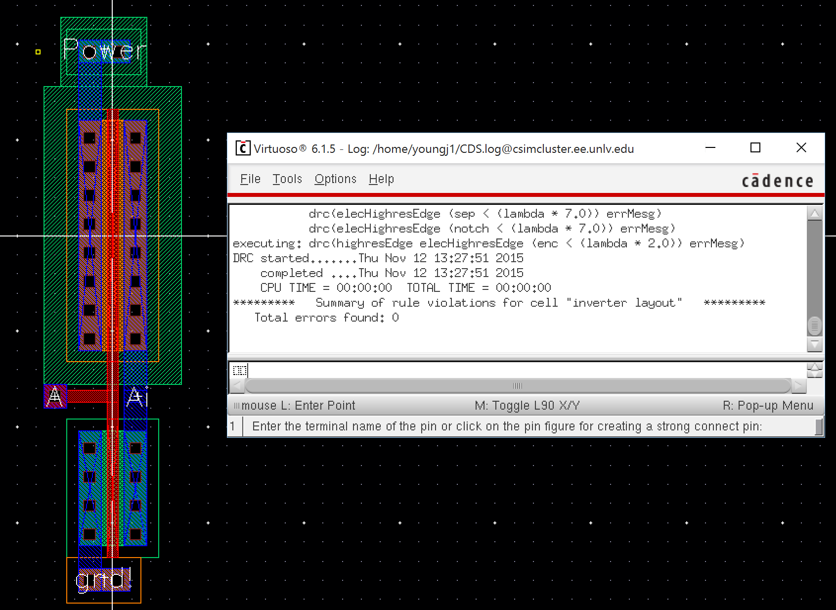
Layout 7:
This image is the layout of the inverter.. It also shows that the layout DRCed without errors.
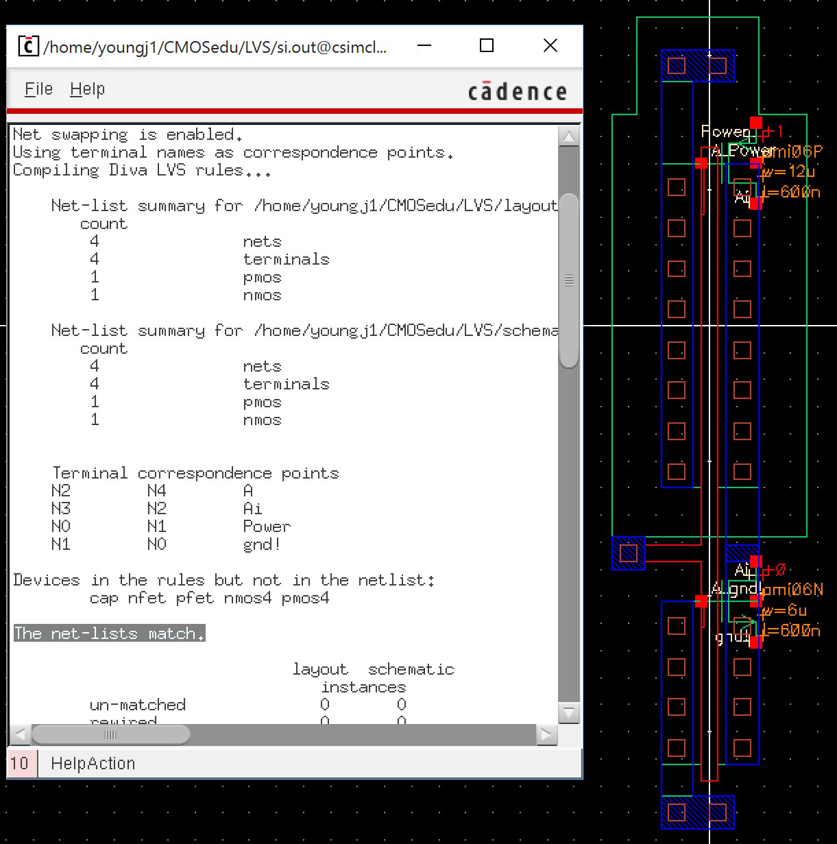
Layout 8:
This is the extracted layout of the inverter seen in Layout 7. It shows that LVS performed without errors.
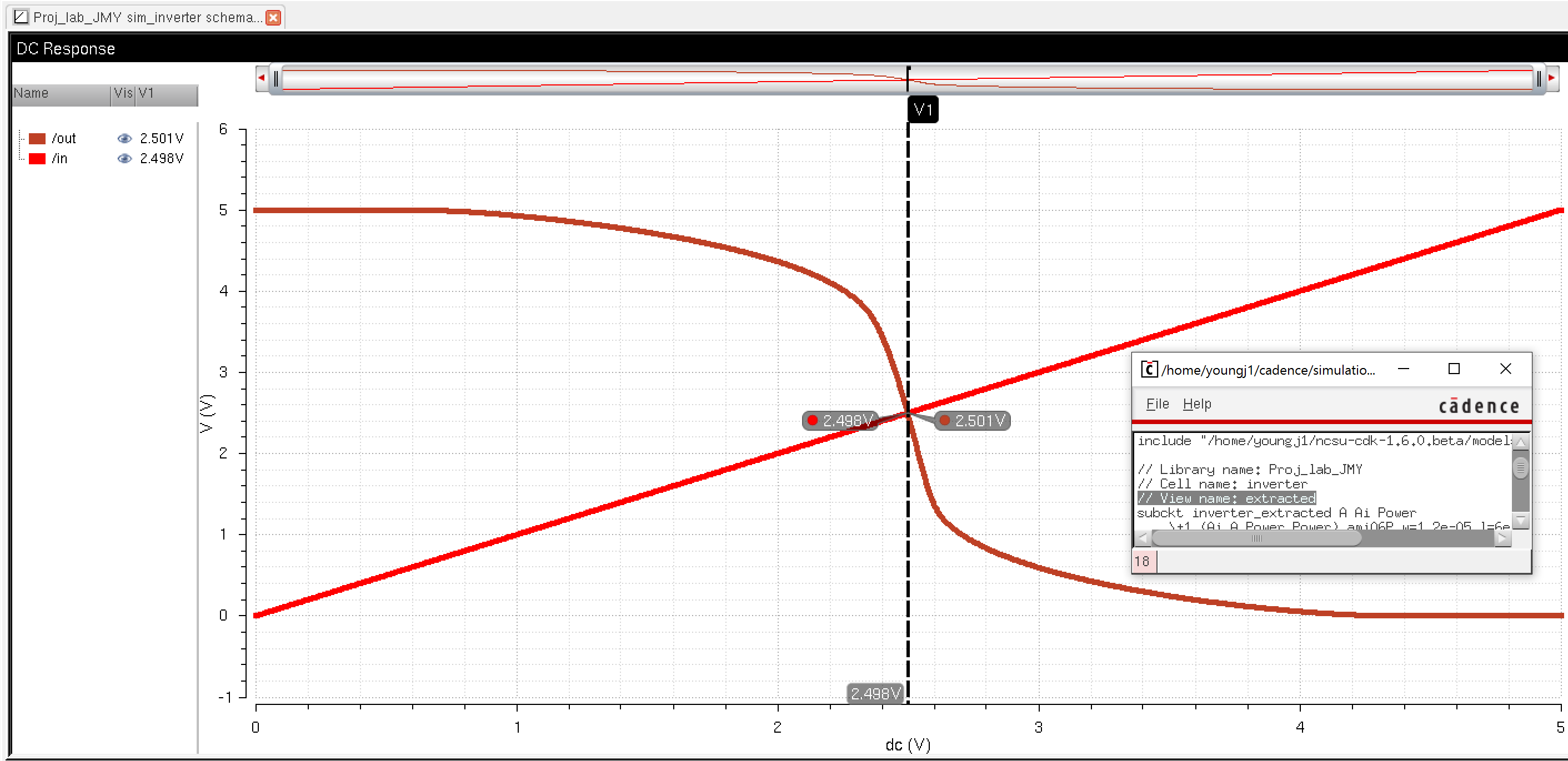
Layout 9:
This is an extracted simulation result using the layout of the circuit in Layout 8 to compare to the simulation of the schematic in Figure 16.
NAND Gate:
The NAND implements the opposite of an AND gate, which means that every input that is not all high will output a high signal.
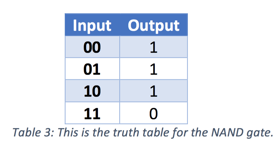
The truth table for a NAND gate is as follows:
Figure 19:
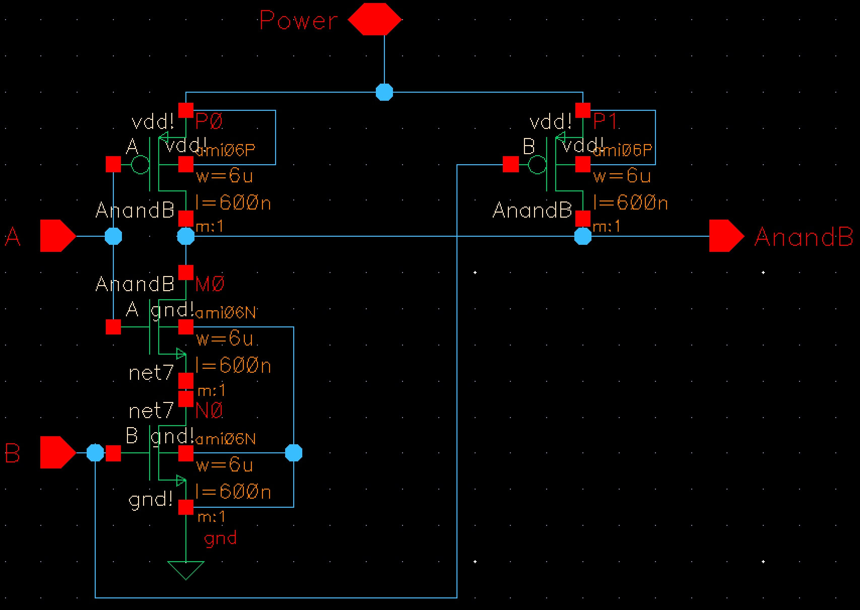
This is the schematic for a NAND gate, using CMOS devices.
Figure 20:
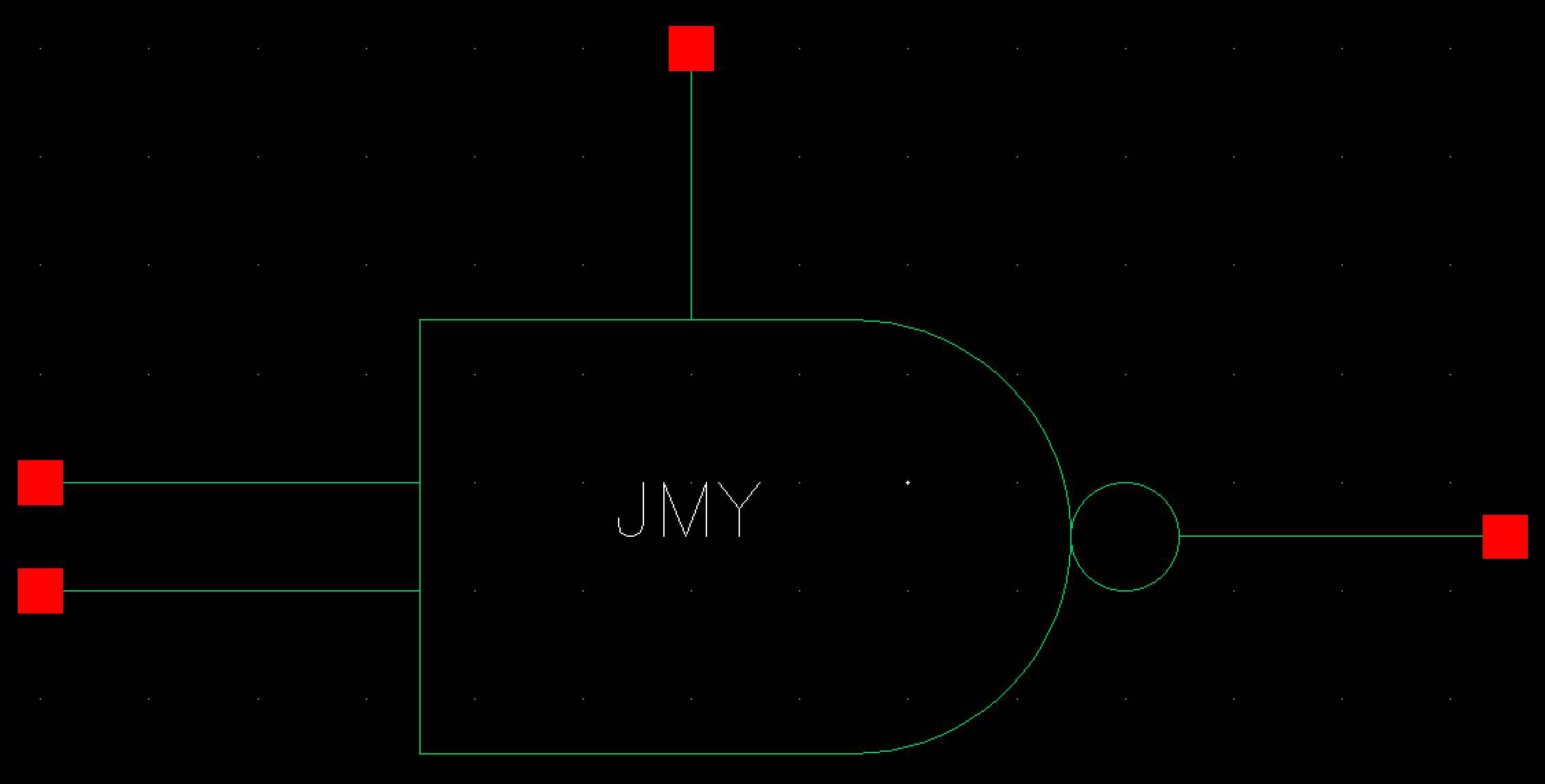
This is a standard symbol for the NAND gate.
Figure 21:
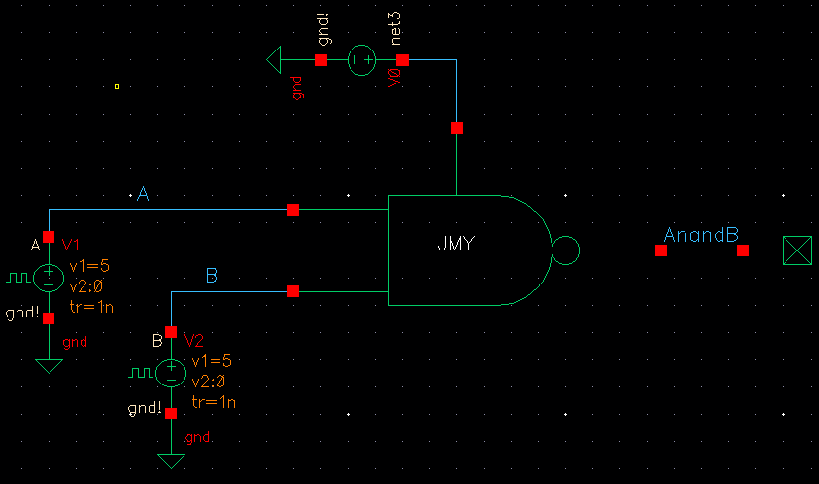
This is a simulation schematic for the NAND gate to test its functionality.
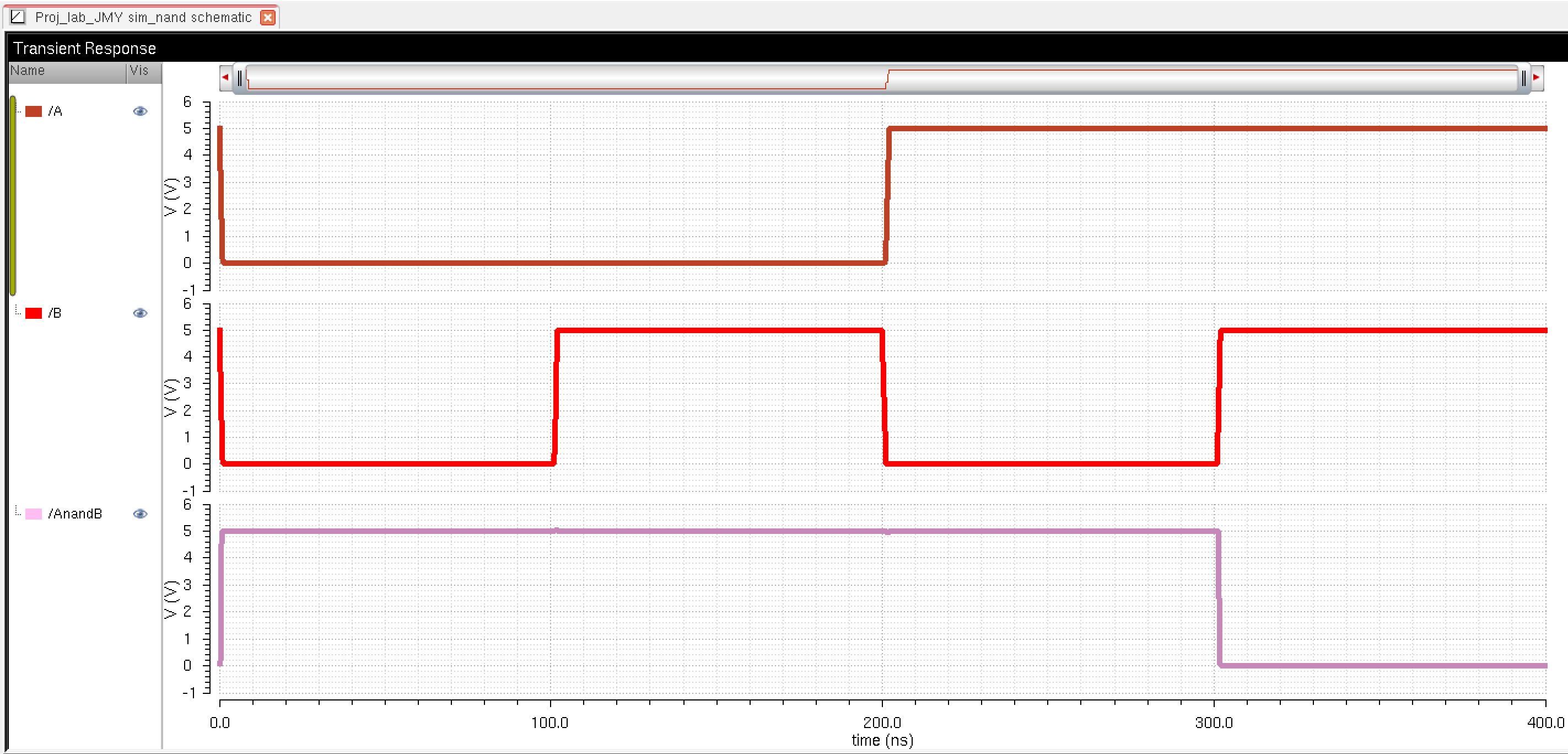
Figure 22:
This is the simulation which was produced from figure 21. Note: The NAND gate goes through all four states, as given in truth table 3 and thus performs as expected.
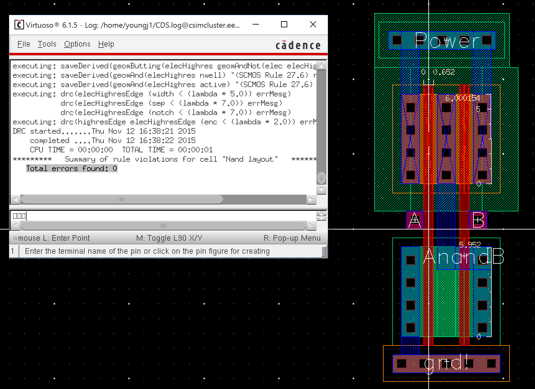
Layout 10:
This image is the layout of the NAND gate. It also shows that the layout DRCed without errors.
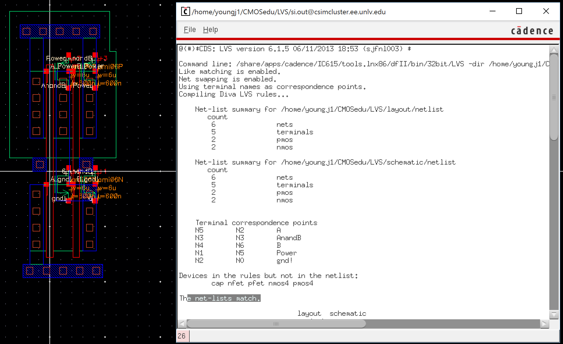
Layout 11:
This is the extracted layout of the NAND gate seen in Layout 10. It shows that LVS performed without errors.
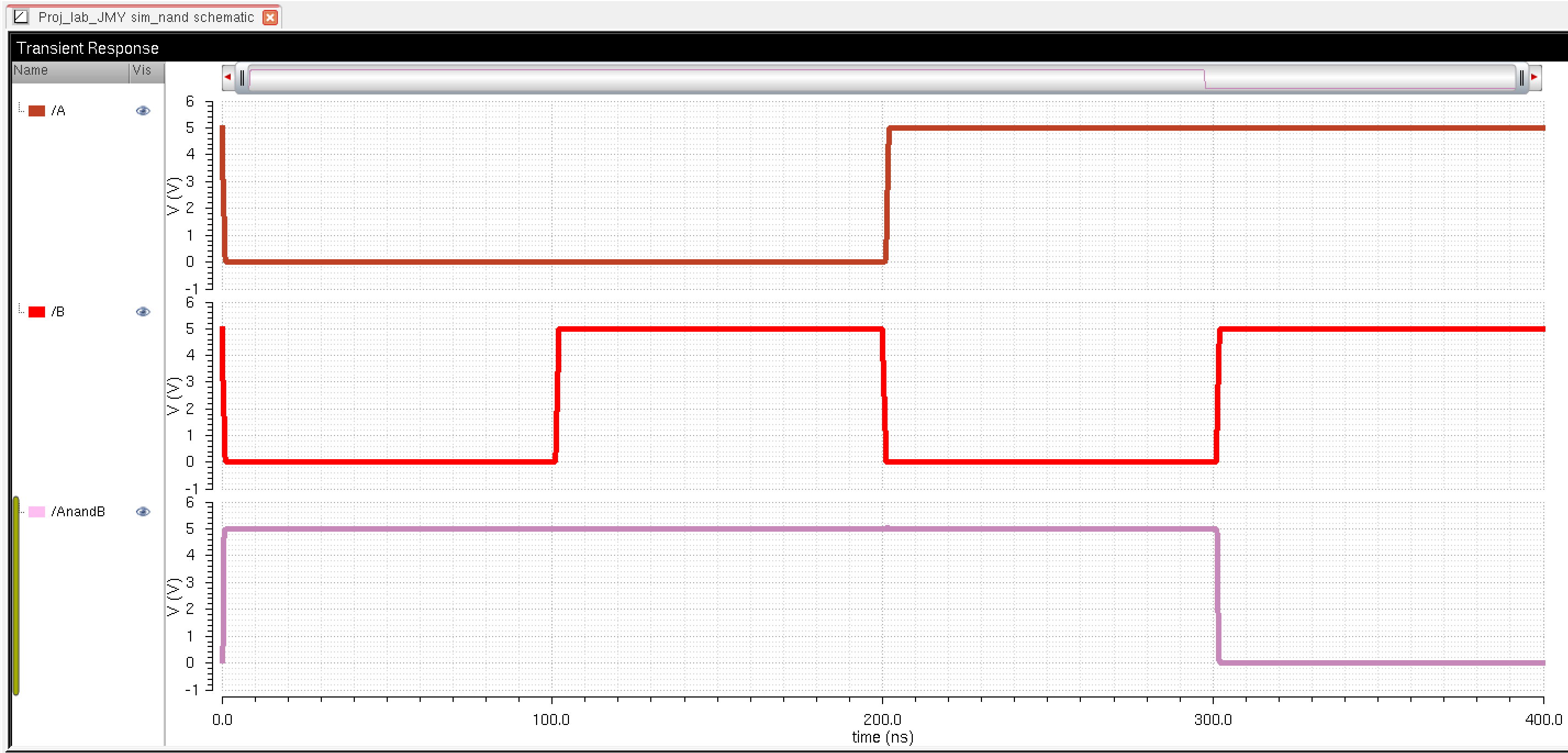
Layout 12:
This is an extracted simulation result using the layout of the circuit in Layout 11 to compare to the simulation of the schematic in Figure 22.
NOR Gate:
The NOR gate implements the inverse of an OR gate, which means when all input lines are low its output will be high. When the input is anything else the output will be low.
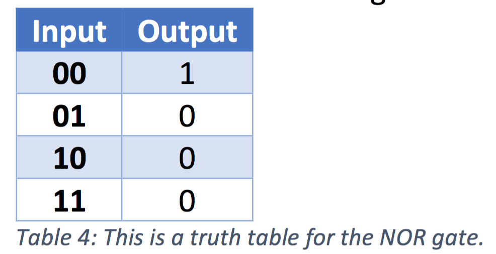
The truth table for a NOR gate is as follows:
Figure 23:
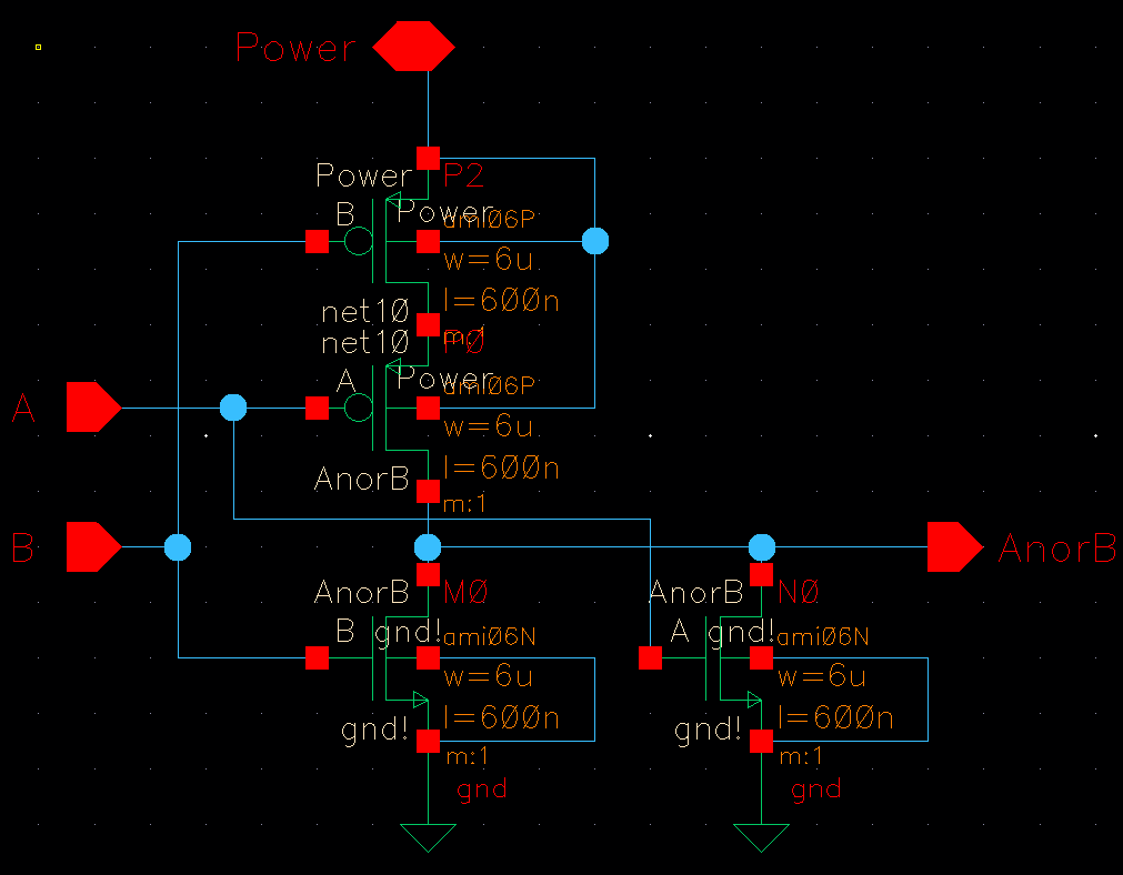
This is the schematic of a NOR gate created with CMOS devices.
Figure 24:
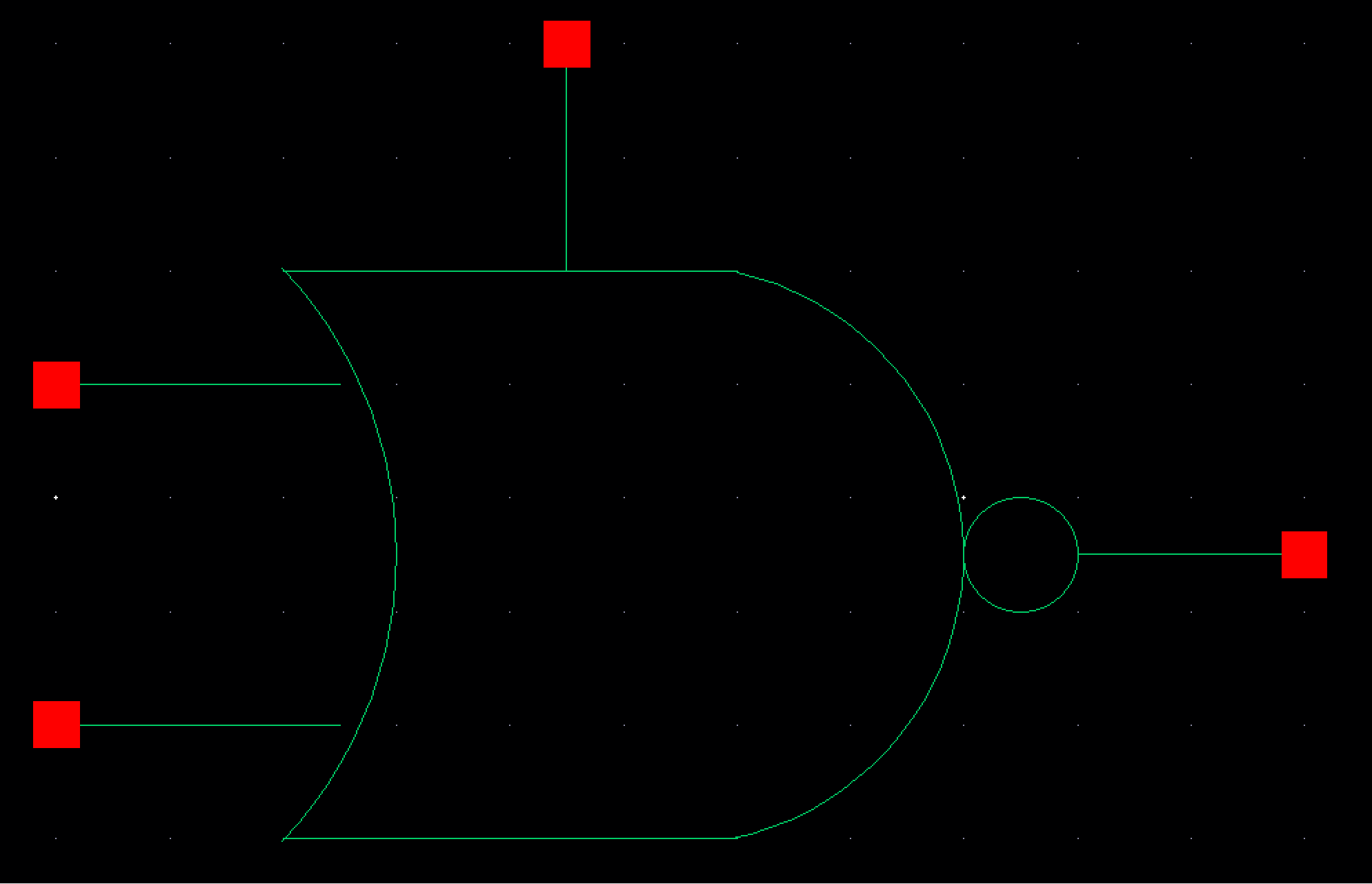
This is a standard NOR gate symbol.
Figure 25:
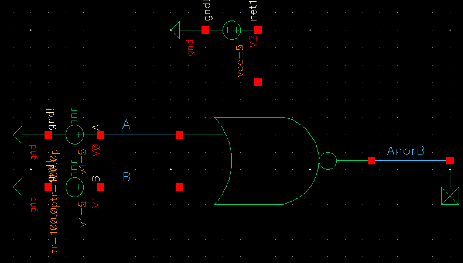
This is the simulation schematic used to verify the circuit's functionality.
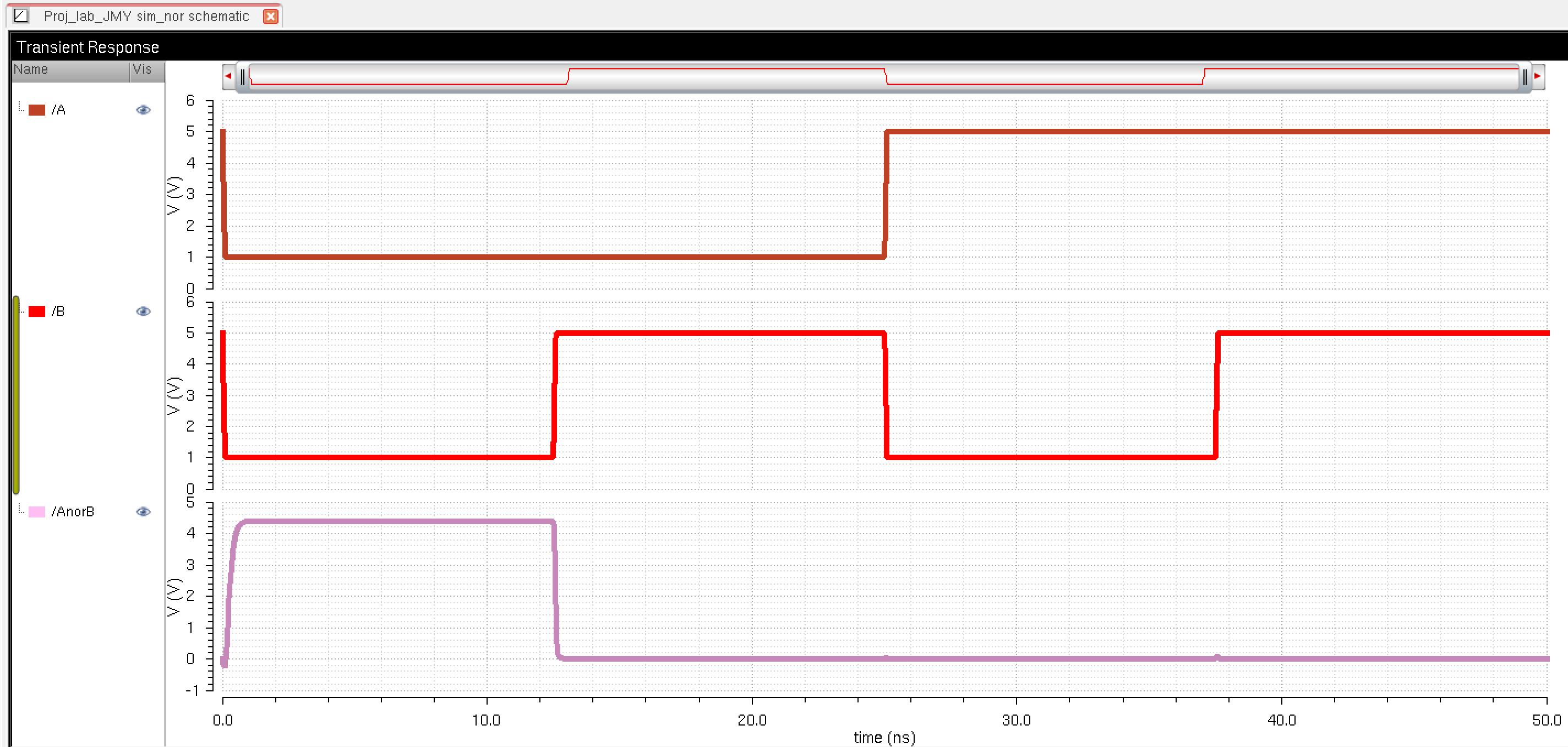
Figure 26:
These are the simulation results produced from figure 25. Note: The simulation simulates all four-states of truth table 4.
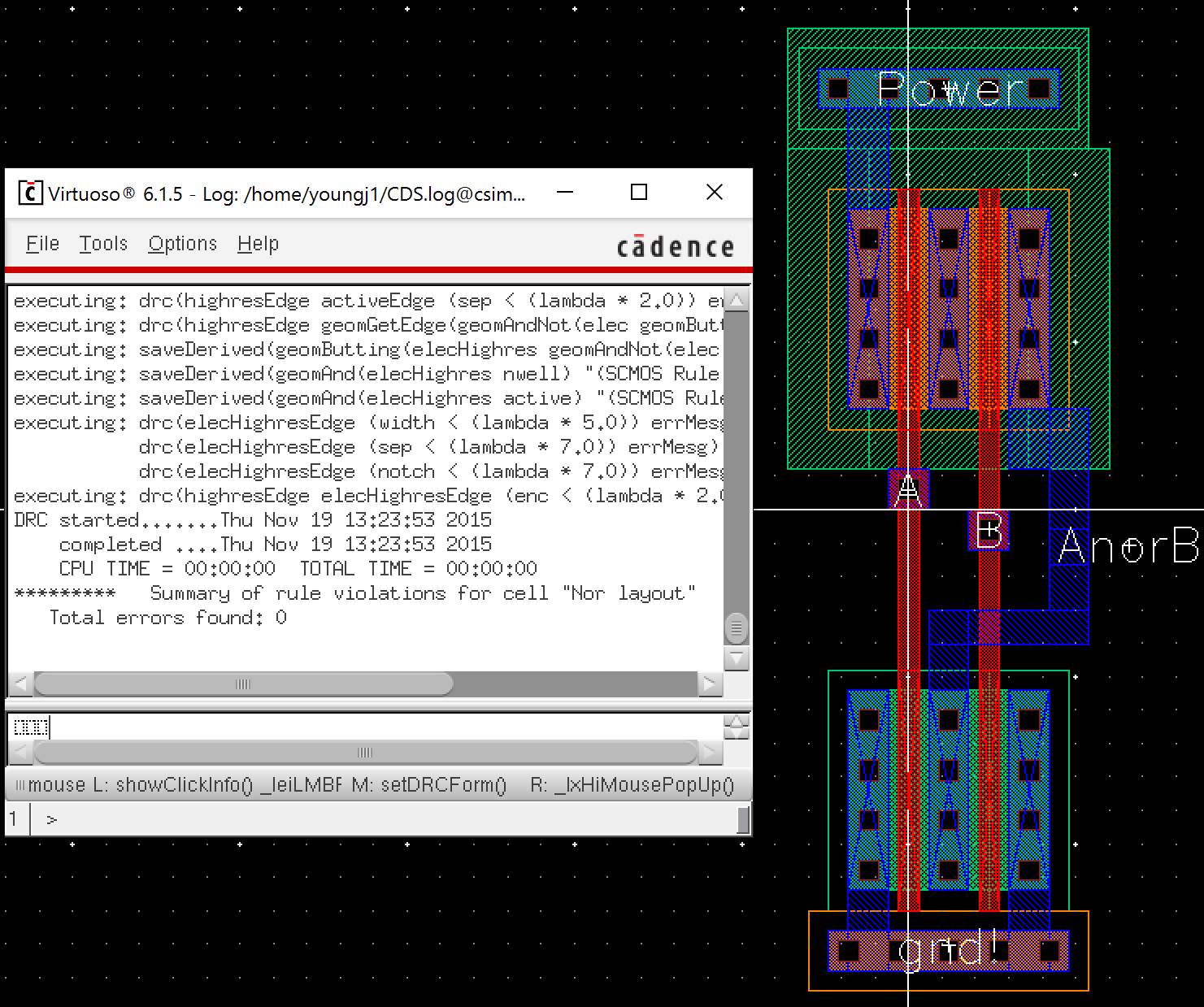
Layout 13:
This image is the layout of the NOR gate. It also shows that the layout DRCed without errors.
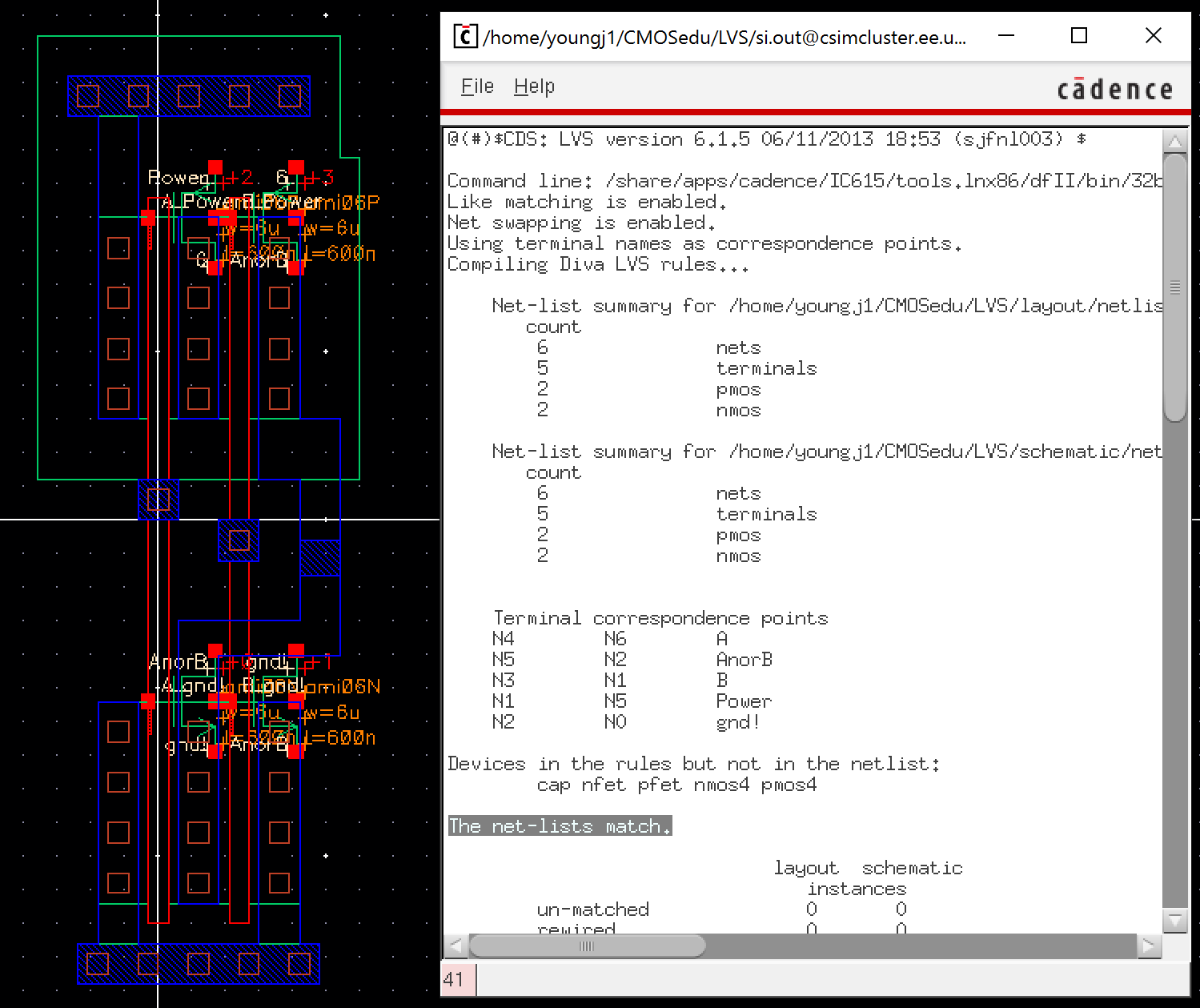
Layout 14:
This is the extracted layout of the NOR gate seen in Layout 13. It shows that LVS performed without errors.
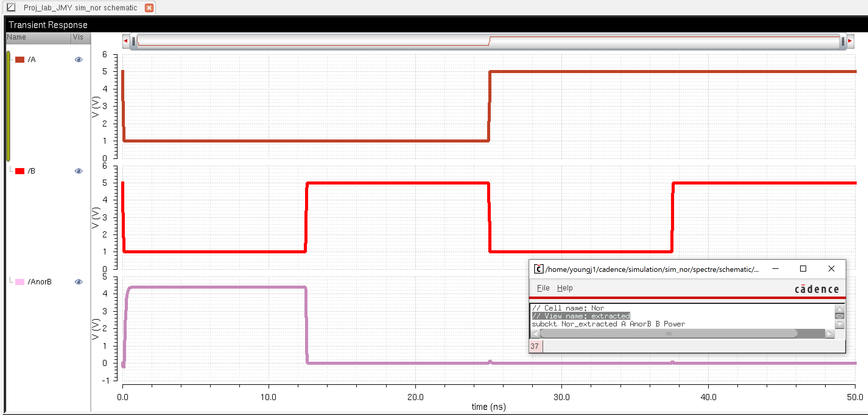
Layout 15:
This is an extracted simulation result using the layout of the circuit in Layout 14 to compare to the simulation of the schematic in Figure 26.
Ring Oscillator:
A ring oscillator is a convenient way of generating a clock signal using only the basic inverter circuit. A ring oscillator is an a-stable device that will oscillate spontaneously with the application of power to the circuit. It comprises "n" gates connected in a string with the output of the last gate fed back as the input to the first. The number of gates must always be an odd value because feeding the output of an inverter back to the input creates an unstable condition; whereas, if you feed the output of a two inverter chain back to the input it will settle high or low after power turn on and not oscillate because this configuration is inherently stable. In a ring oscillator, the state of the last gate depends on the state of the first gate and vice- versa but due to the cumulative delay of the inverter chain the state changes will occur at intervals equal to the cumulative time delay of the chain, so, the device oscillates at a frequency driven by 1/n*d where "n" is the number of inverters and "d" is the sum of the individual delay times for an inverter. Note: That if one increases the number of inverters the resultant frequency will be lower and if one decreases the number inverters the frequency will be higher so a wide range of frequencies can be achieved with this simple design.
Since one of the design requirements for this project is to design a 31-stage ring oscillator, 31 inverters will be used. Another requirement is that this oscillator must have a buffered connection that is capable of driving a 20pF load, see the discussion in the buffer section above for more information.
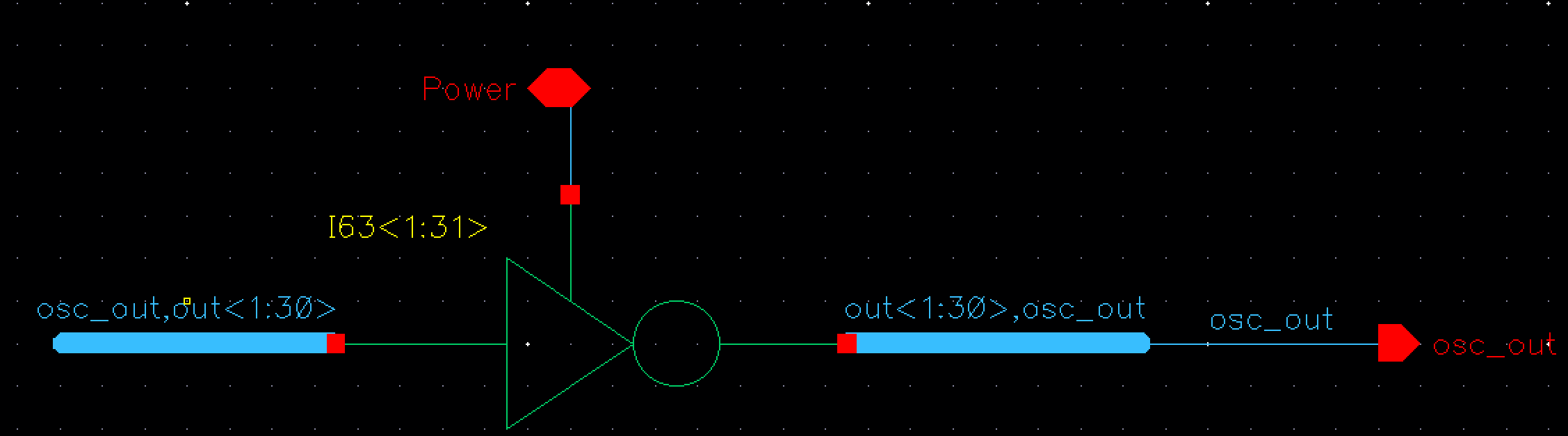
Figure 27:
This is the schematic of a ring oscillator. Note: This is using 31 invertors, which are instantiated 31 times. The inverter schematic was generated above.
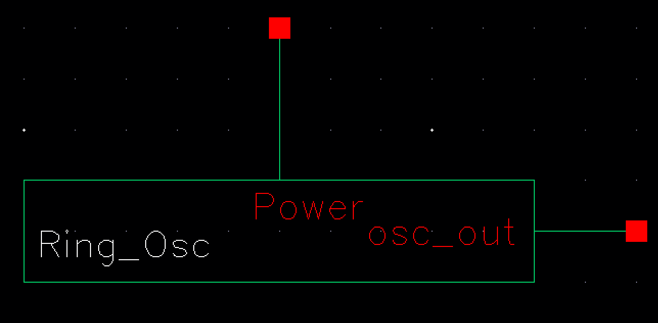
Figure 28:
This is the created symbol of a ring oscillator.
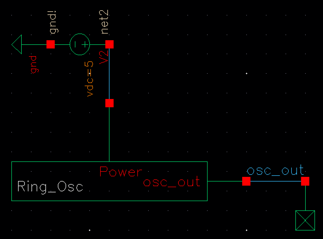
Figure 29:
This is the simulation schematic to test functionality of the ring oscillator to ensure it oscillates.
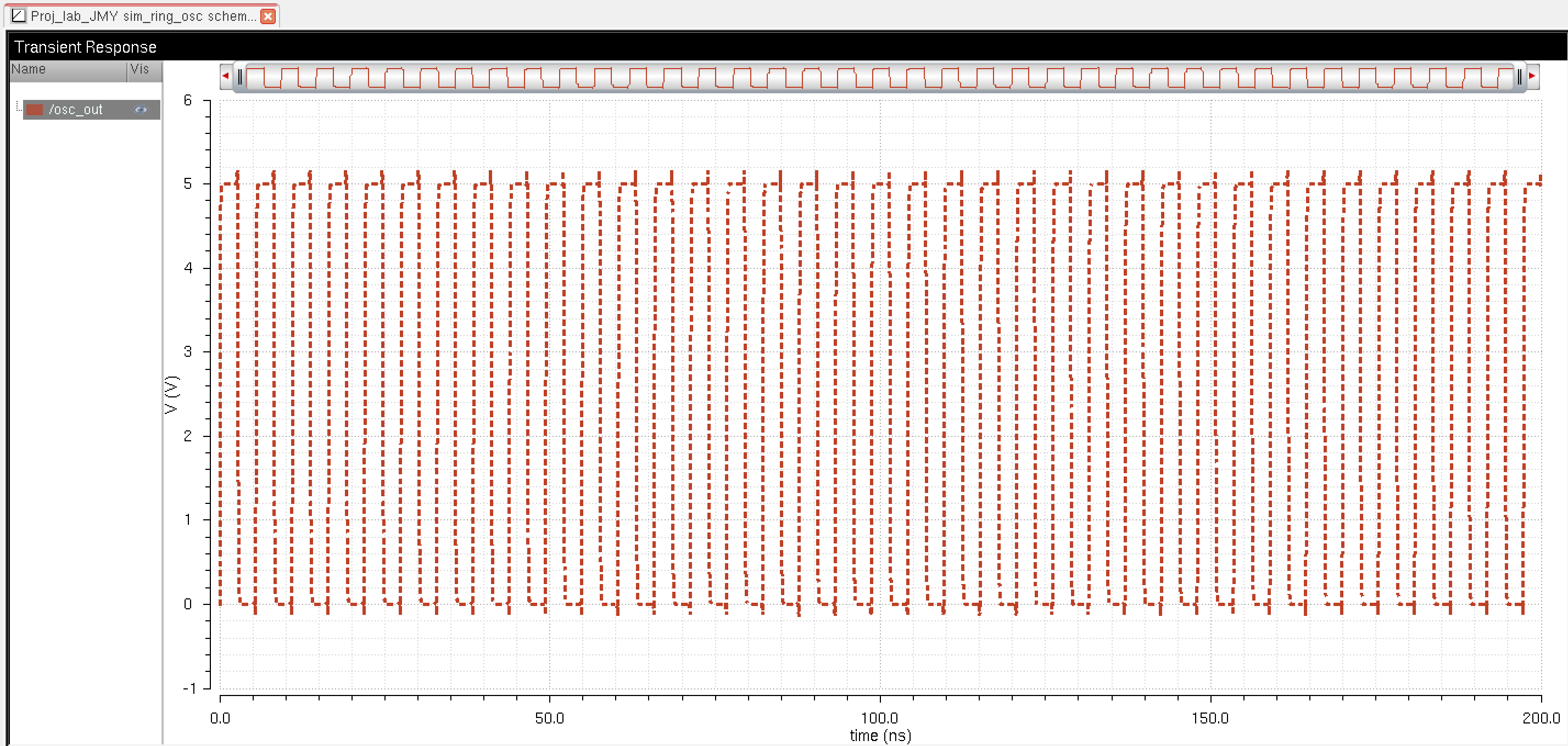
Figure 30:
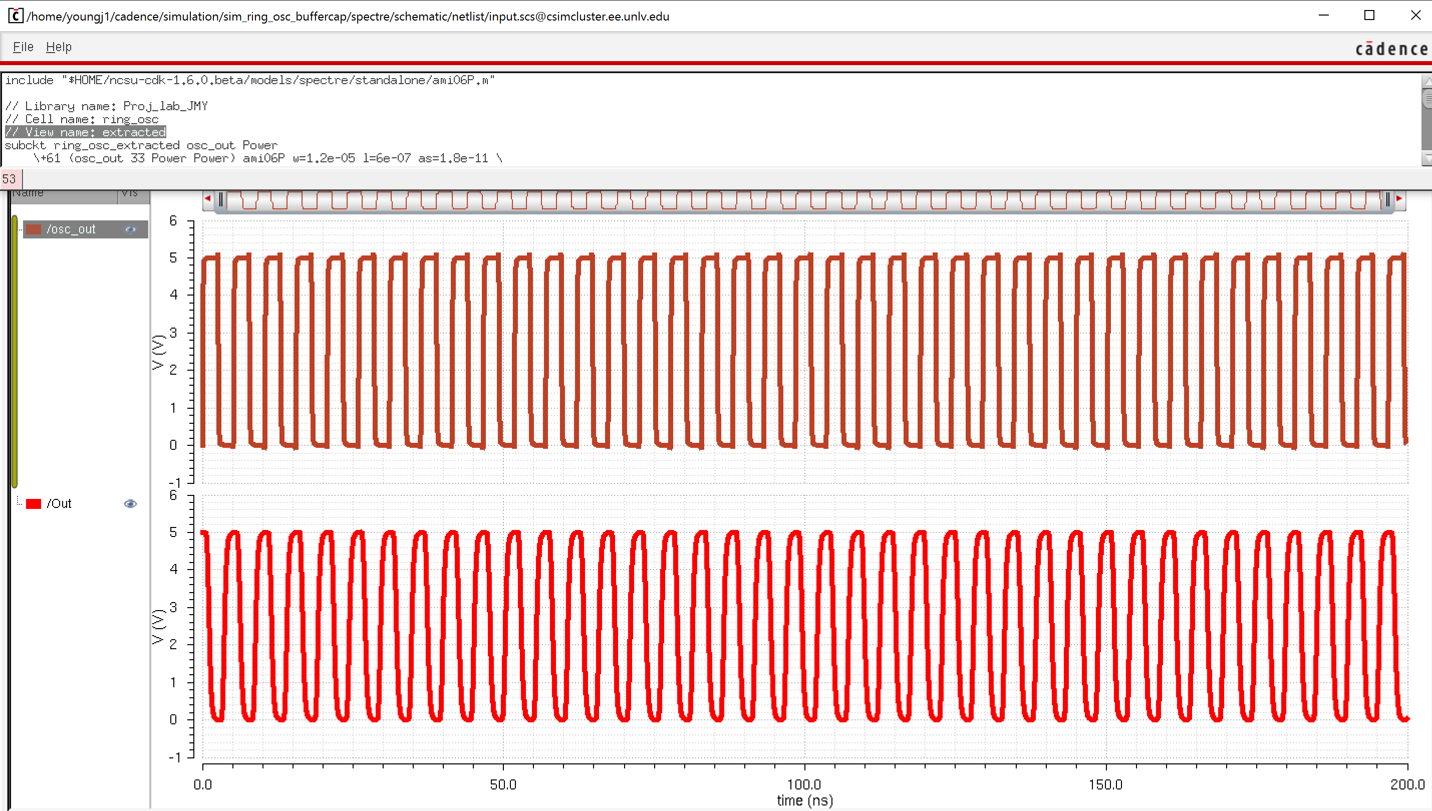
This is the simulation of the schematic in figure 31, showing proper oscillation. Note: Using the C5 process, the oscillation should be 1/31*189ps (delay, using values in the buffer gate section) =170.6 MHz which is close to the simulation results here which appear to be in the range of 200 MHz.
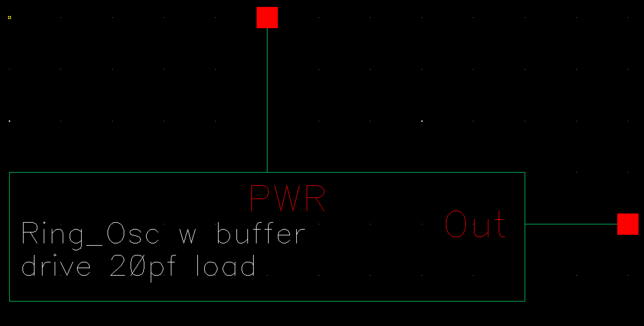
Figure 31:
This is another simulation schematic, but this time with a buffer and a 20pF load as per the project's design requirements. Note: The symbol below will be just the Ring_Osc and Buffer connection combined.
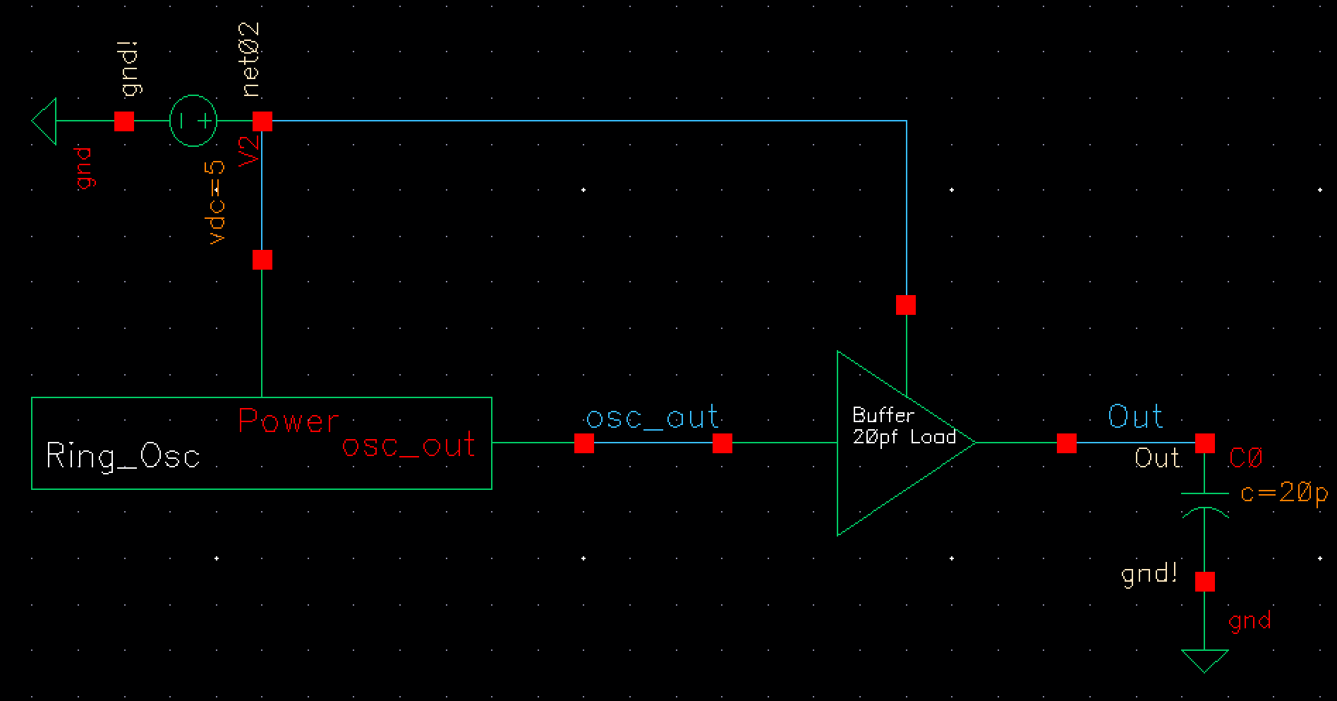
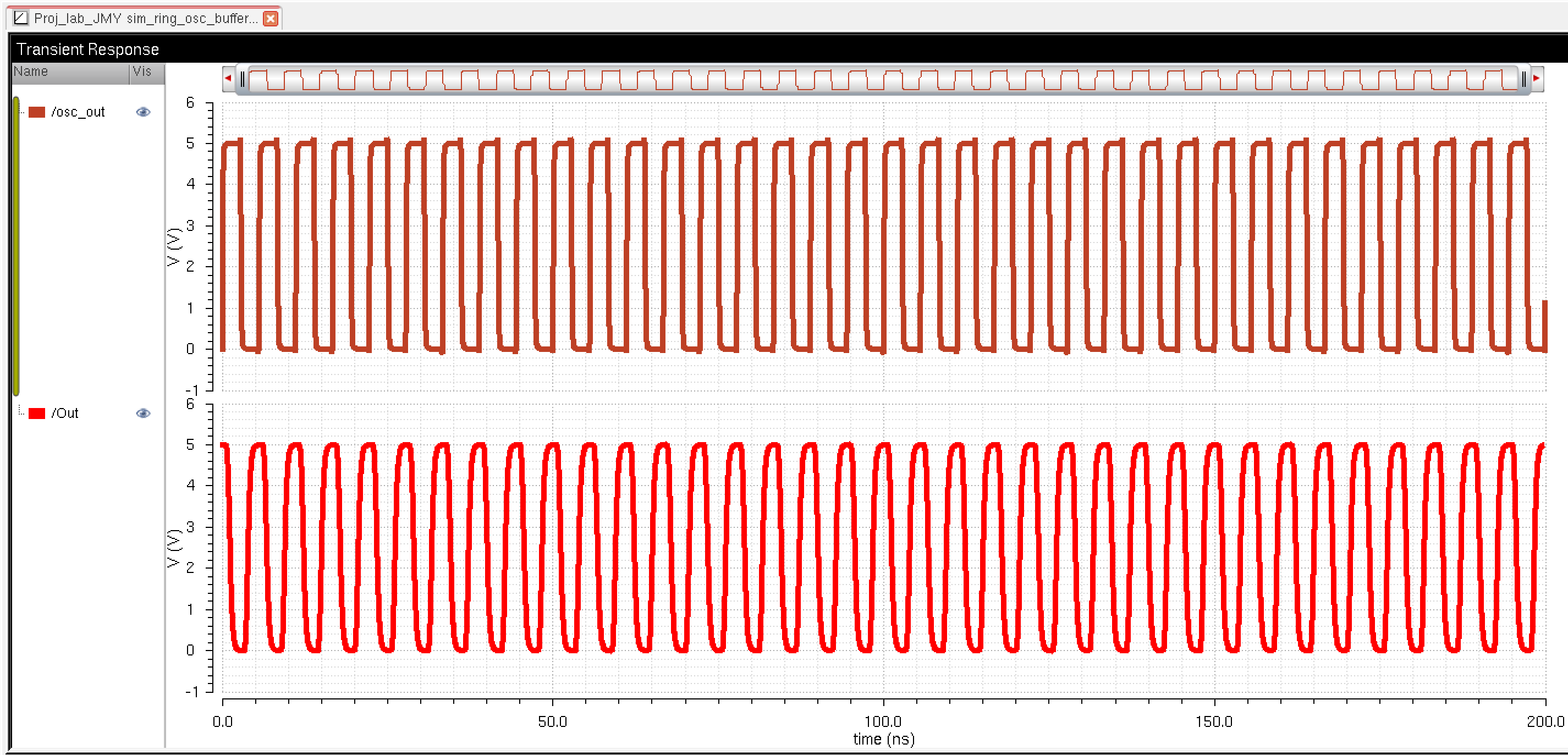
Figure 32:
These are the simulation results of figure 31, showing how the output is unaffected by the 20pF load, i.e. the signal continues to oscillate without change.
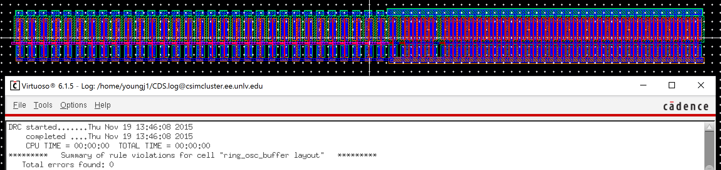
Layout 16:
This image is the layout of the ring oscillator with a buffer. It also shows that the layout DRCed without errors. Note: These layouts are with the ring oscillator and buffer, as per the design requirements.
Layout 17:
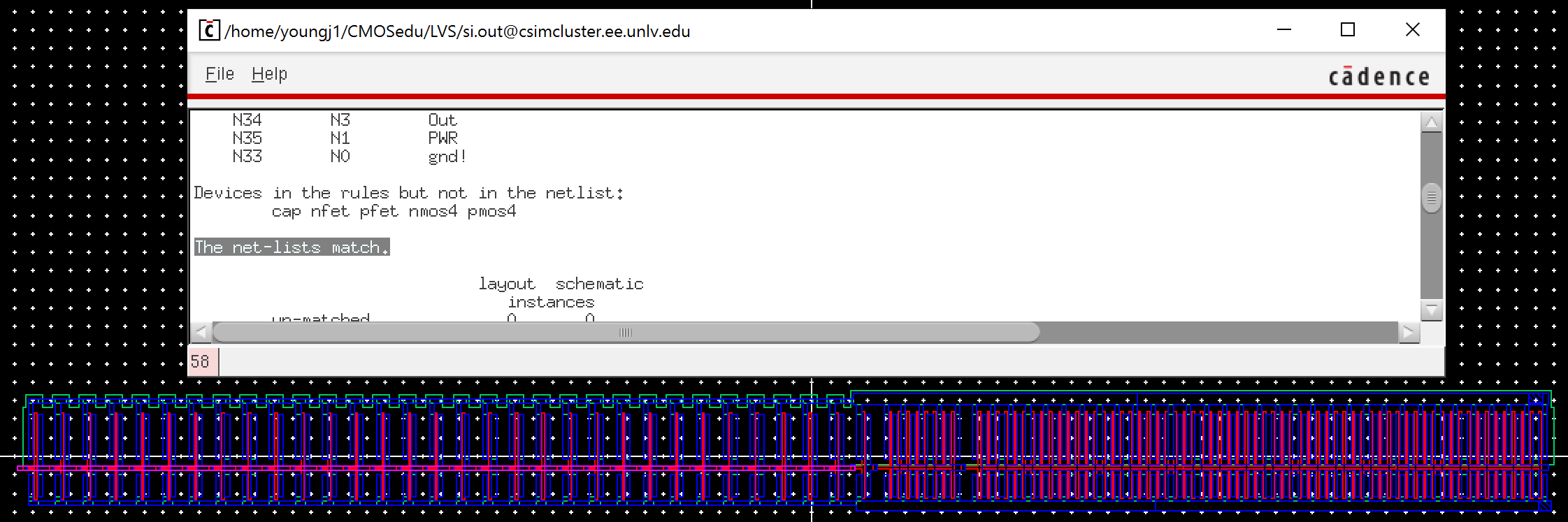
This is the extracted layout of the ring oscillator with a buffer seen in Layout 16. It shows that LVS performed without errors.
Layout 18:
This is an extracted simulation result using the layout of the circuit in Layout 17 to compare to the simulation of the schematic in Figure 32.
Transmission Gate:
Transmission gates are created with the CMOS devices connected end to end, as seen in the schematic below. This allows the control signals (gate inputs) to allow signals through their respective gates. Both the connections will be input and output. The functionality of this circuit works for example of the up/down counter, the up signal is the control signal with the input and output signals driving clocks or input into the D FF with clear.
If the up signal is high, then the output will be allowed through the NMOS device but not the PMOS device. If the up signal is low, for a count down, then the PMOS is on and allows signal to propagate through the transistors. This design allows one to implement straight logic functions which control the flow of input and output signals to their respective circuit counter part.
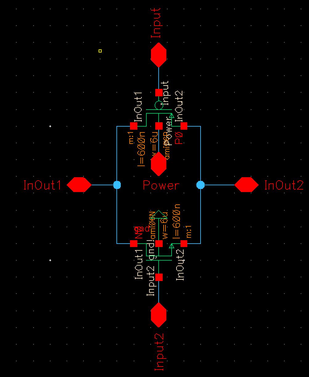
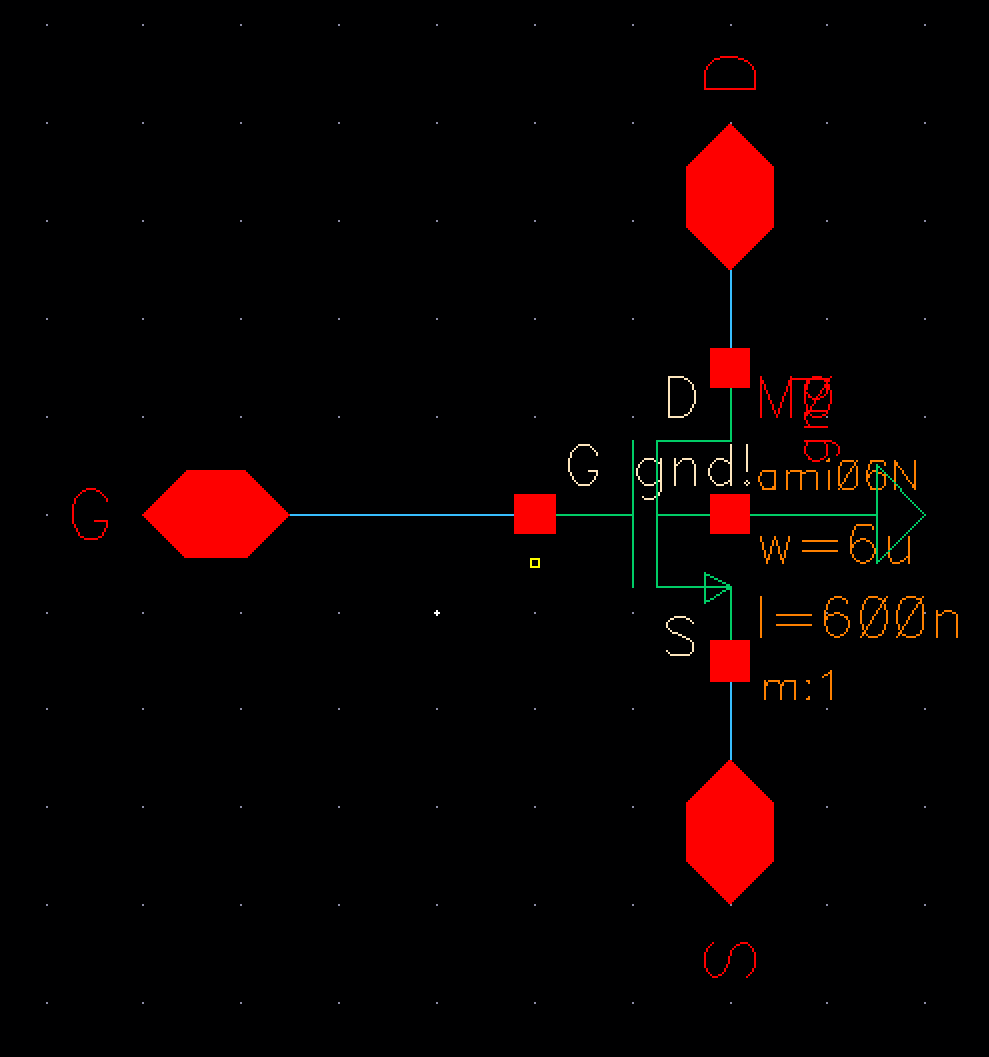
Figure 33:
This is the schematic of a transmission gate.
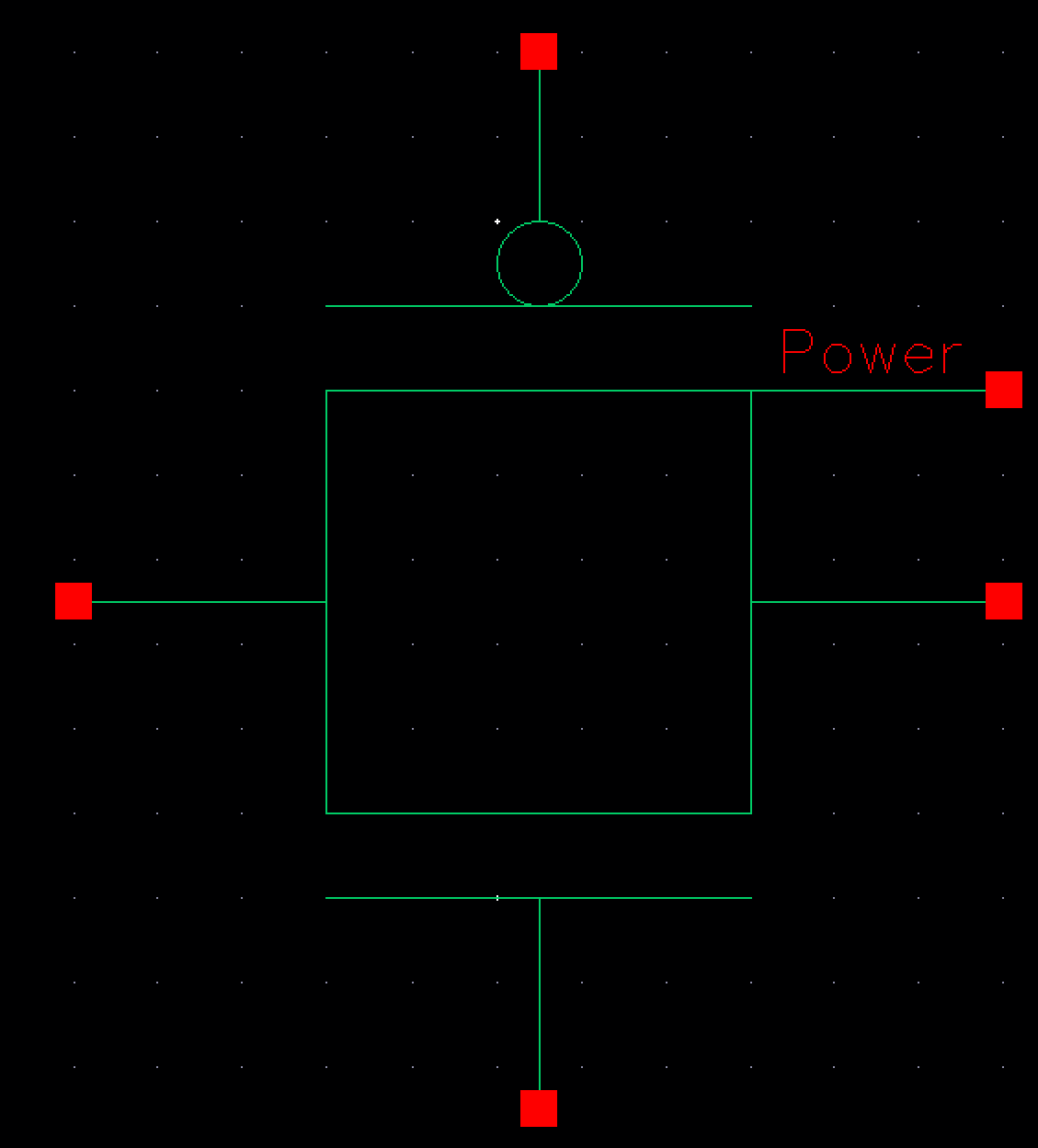
Figure 34:
This is a standard symbol for a transmission gate.
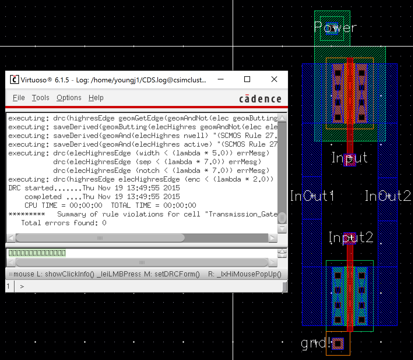
Layout 19:
This image is the layout of the transmission gate. It also shows that the layout DRCed without errors.
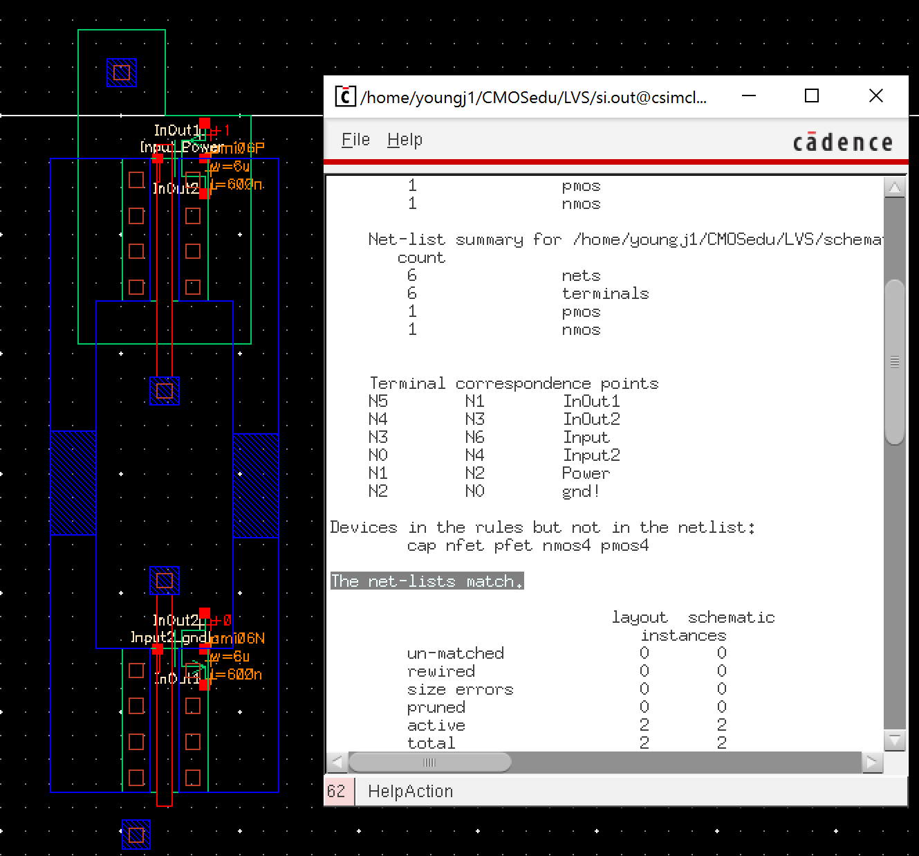
Layout 20:
This is the extracted layout of the transmission gate seen in Layout 19. It shows that LVS performed without errors.
Transistors (NMOS/PMOS):
The negative metal oxide semiconductor (NMOS) transistor is part of the complementary metal oxide semiconductors, it's opposite is the positive metal oxide semiconductor (PMOS). These devices are opposites of each other, meaning that when one gate is active the other gate will be off when they are used in conjunction with each other in circuit designs, such as the inverter design above. The NMOS allows signal to propagate from the drain (top of the device, D) down to the supply (which is often connected directly to ground, S), when the gate (middle input pin, G) is has a signal about its threshold voltage. The threshold voltage is the amount of voltage required for an input signal to overcome before the gate (switch) is activated. The PMOS on the other hand has its supply on top, with the drain on the bottom. This is opposite the NMOS. Also note that the gate leading into the PMOS has a circle, which implies it is inverted and thus the gate activates only when the input signal is low (0). In all, the use of these basic CMOS elements is critical because it allows one to realize every high-level functional design (ring oscillator, counter, etc) on the chip using these elements as basic building blocks. This is what makes the integrated circuit chip possible.
Figure 35:
This is the schematic for an NMOS transistor.
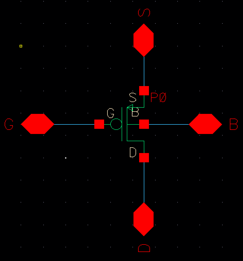
Figure 36:
This is the symbol of an NMOS transistor, note the body is connected to ground and thus is not shown here.
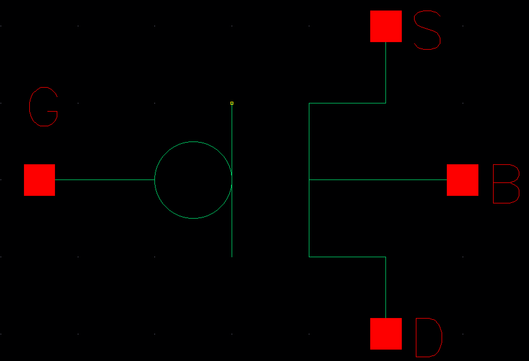
Figure 37:
This is the schematic of a PMOS transistor, note the body is a pin to allow it to be connected to a separate power line.
Figure 38:
This is the standard symbol for the PMOS transistor.
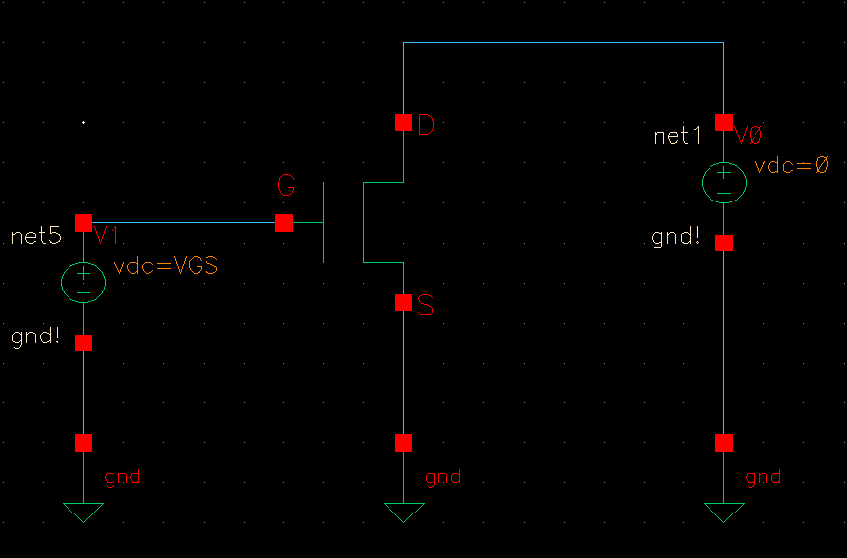
Figure 39:
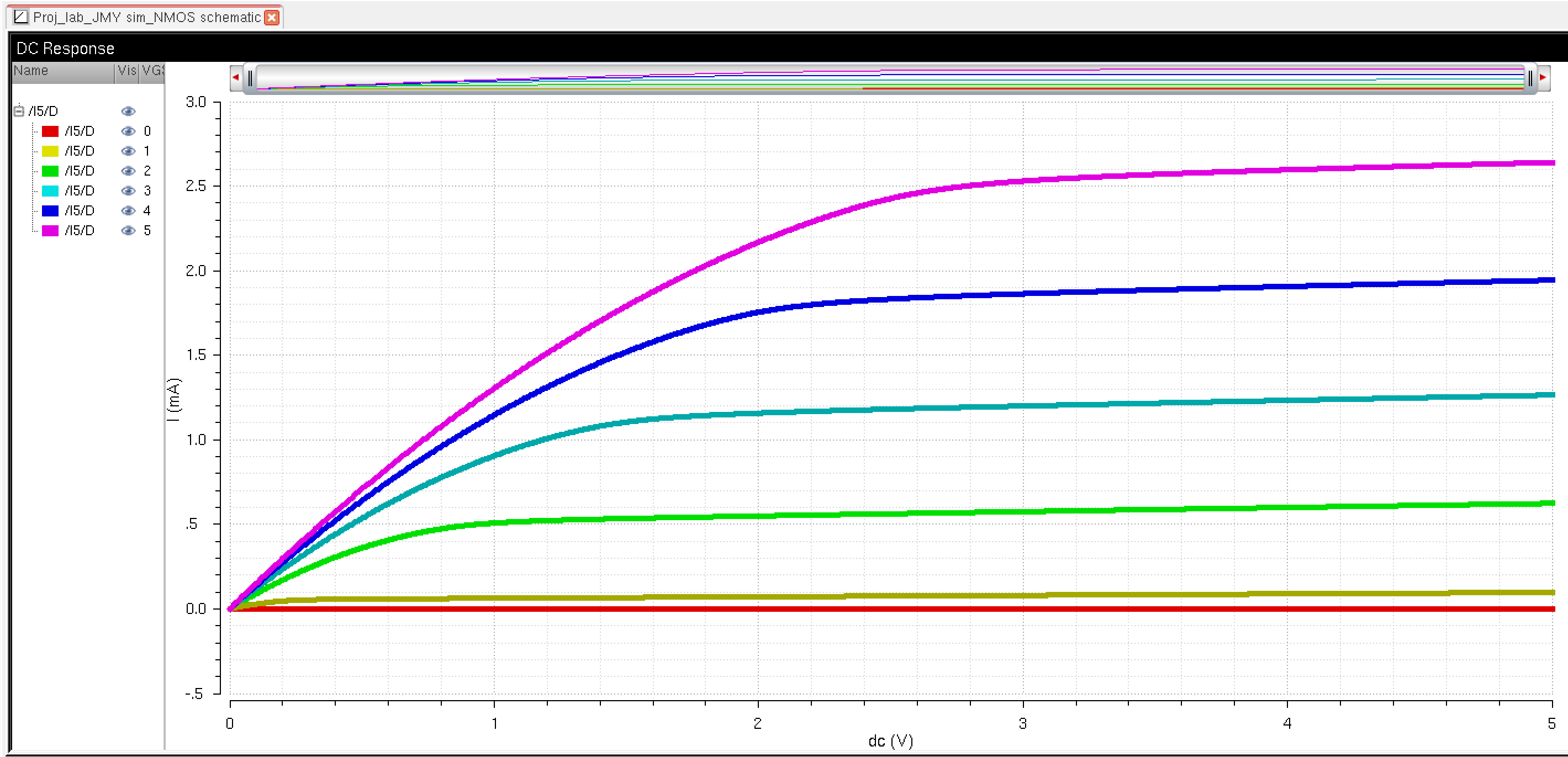
This is the simulation schematic of an NMOS transistor.
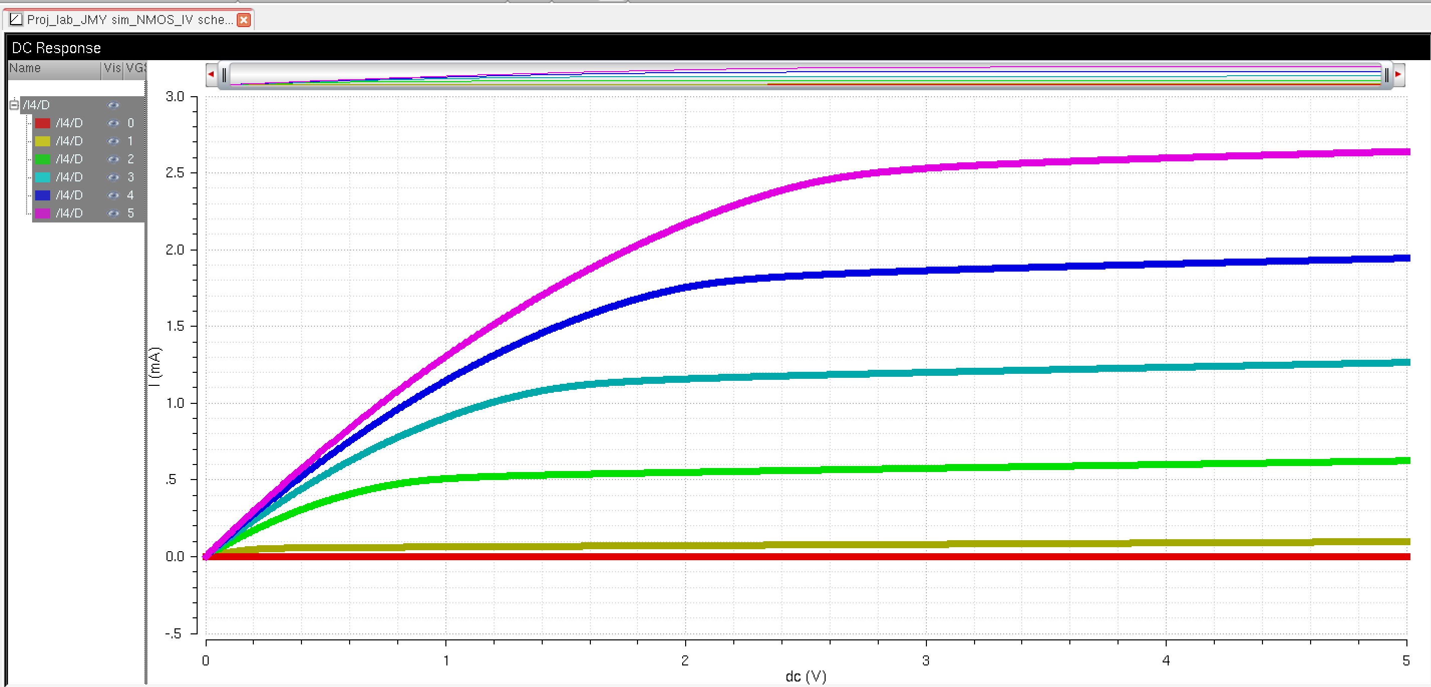
Figure 40:
These are the simulation results produced from the schematic of the previous figure. As Vds increases the higher the output goes, especially in lowering the threshold voltage required to activate the gate of the NMOS transistor.
Figure 41:
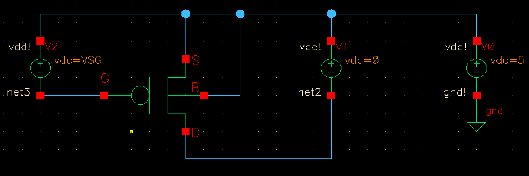
This is the simulation schematic for testing the functionality of the PMOS transistor.
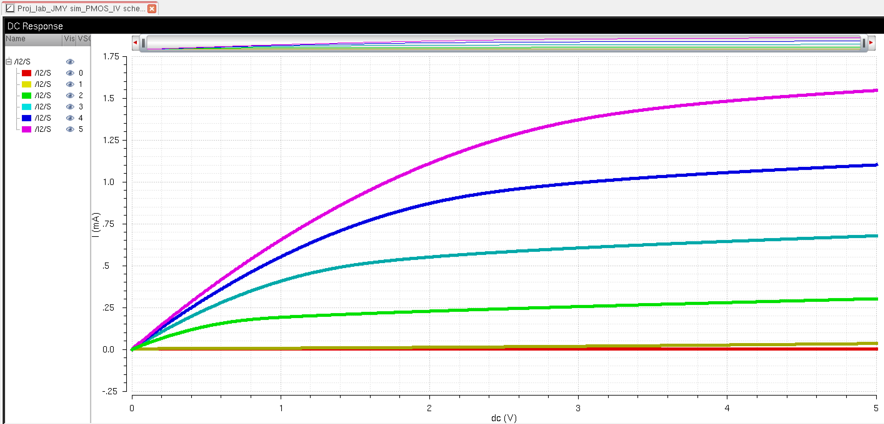
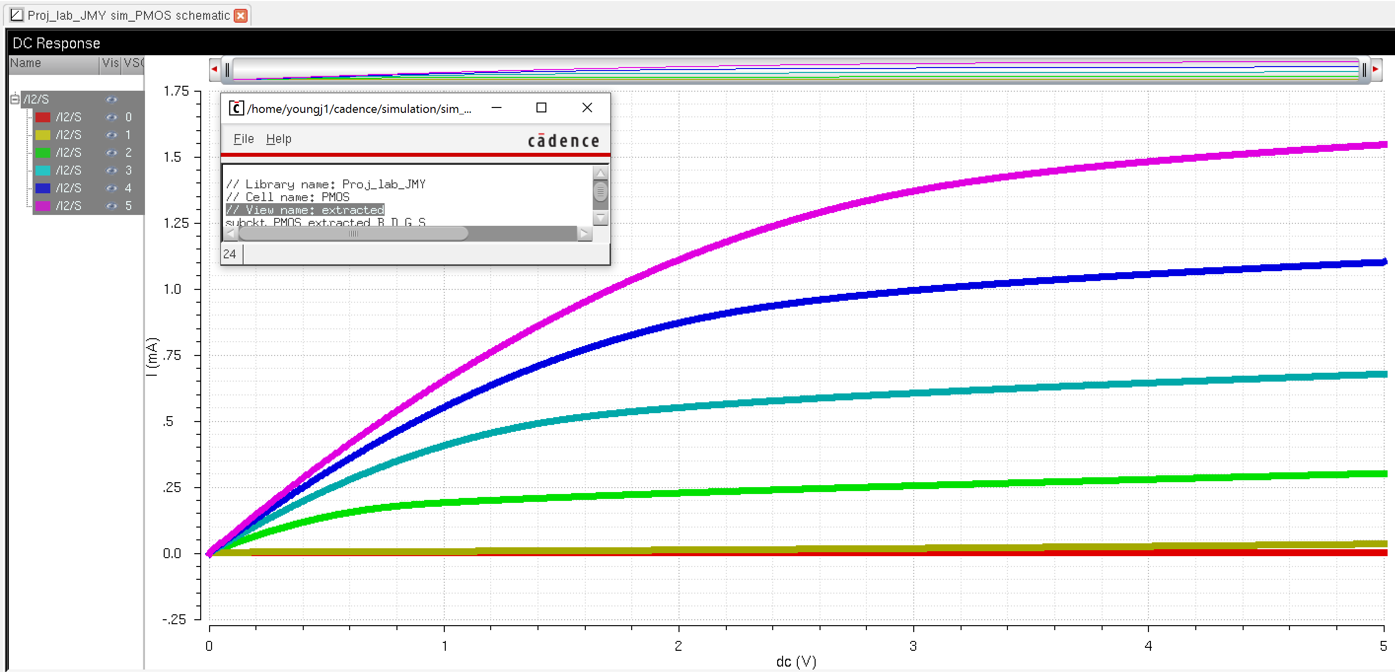
Figure 42:
These are the simulation results produced from the schematic of the previous figure. As Vsd increases the higher the output goes, especially in lowering the threshold voltage required to activate the gate of the PMOS transistor.
Layout 21:
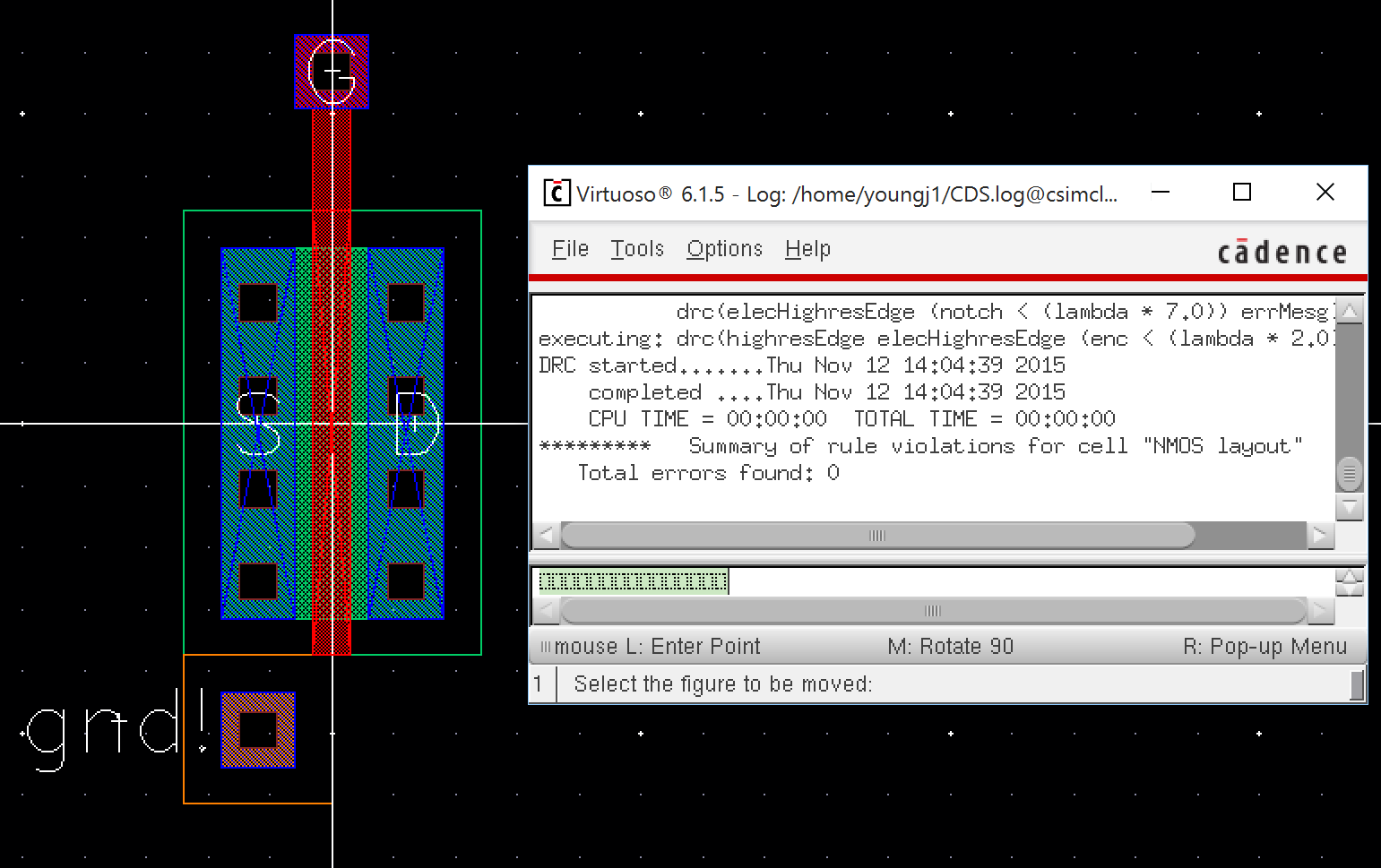
This image is the layout of the NMOS. It also shows that the layout DRCed without errors.
Layout 22:
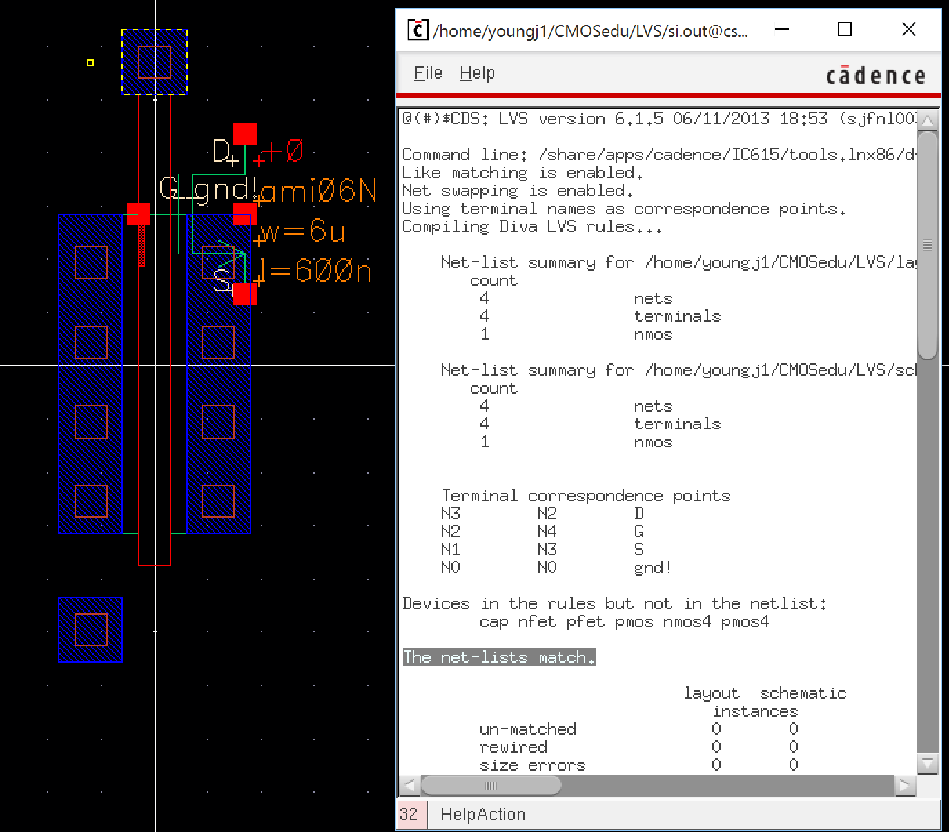
This is the extracted layout of the NMOS seen in Layout 22. It shows that LVS performed without errors.
Layout 23:
This is an extracted simulation result using the layout of the circuit in Layout 23 to compare to the simulation of the schematic in Figure 40.
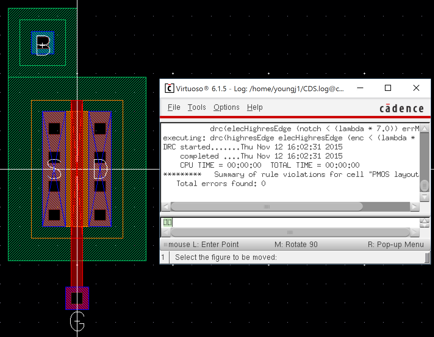
Layout 24:
This image is the layout of the PMOS. It also shows that the layout DRCed without errors.
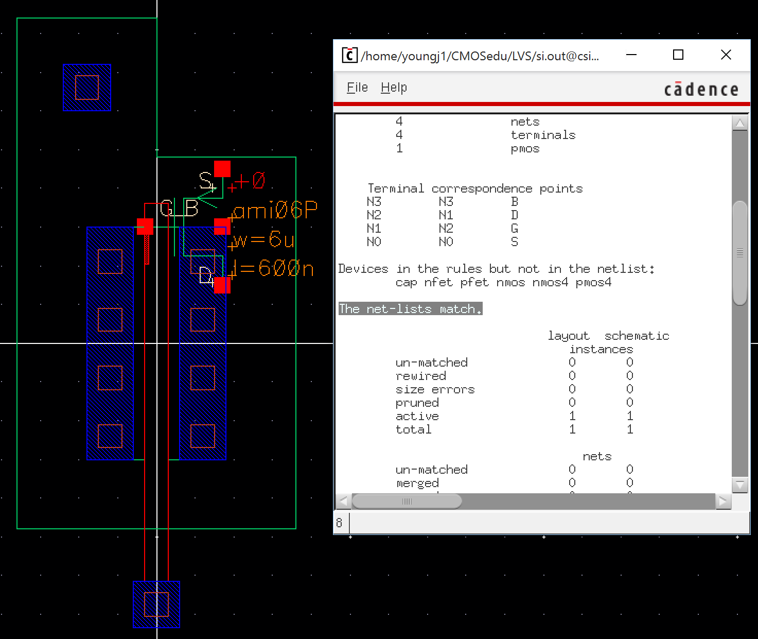
Layout 25:
This is the extracted layout of the PMOS seen in Layout 25. It shows that LVS performed without errors.
Layout 26:
This is an extracted simulation result using the layout of the circuit in Layout 26 to compare to the simulation of the schematic in Figure 42.
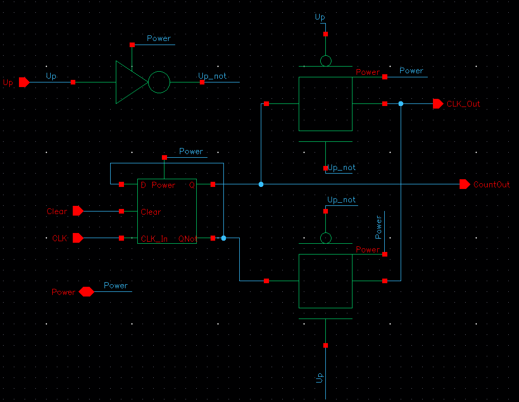
Up/Down Counter:
A single up/down counter consists of the D FF with an asynchronous clear along with two transmission gates, which are connected to the up input signal. This is what gives the up/down counter the ability to count up or down by allowing/blocking the signals that are allowed to transfer through. Once a signal propagates though it is then stored in the D FF. For more information on how the D FF or the D FF with a clear work, see the discussions above.
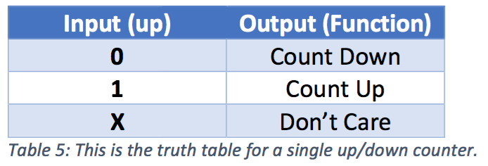
The truth table for the up/down counter is as follows:
Figure 43:
This is the schematic for a single bit up/down counter with a clear.
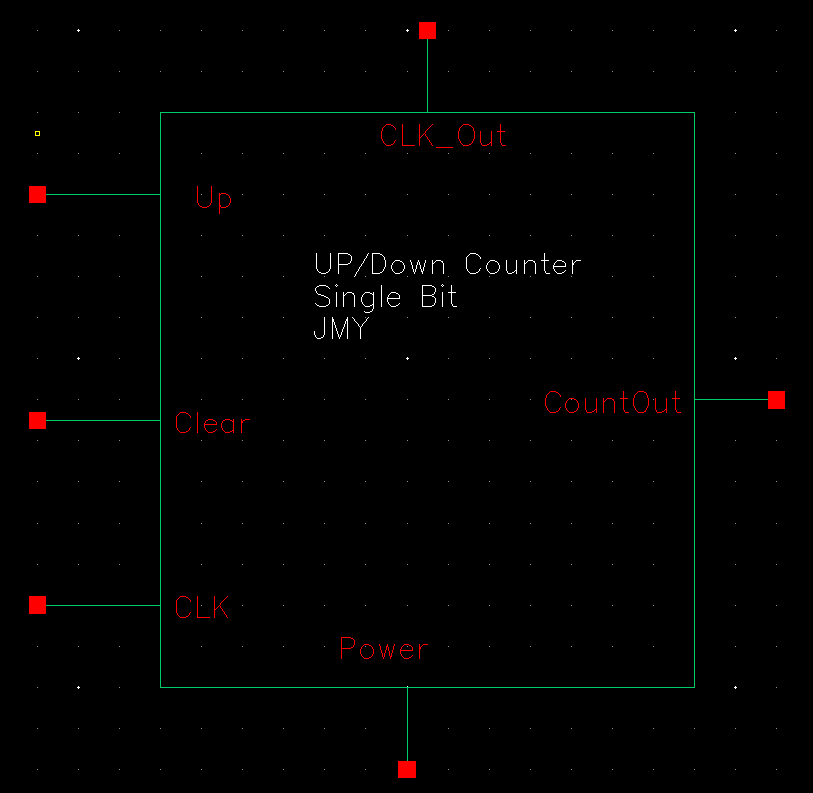
Figure 44:
This is the symbol for an up/down counter with a clear and two outputs.
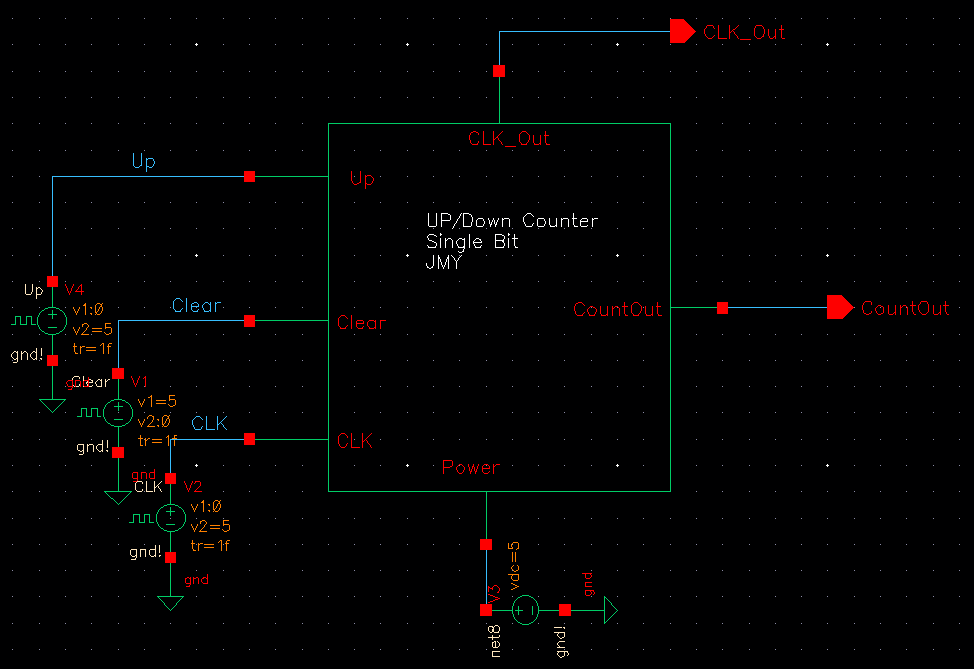
Figure 45:
This is the simulation schematic, which is used to verify the up/down functionality of the counter.
Figure 46:
These are the simulation results from the previous figure, showing how the counter is working with up/down and an active clear. All results are satisfactory.
Layout 27:
This image is the layout of the up/down counter with a clear. It also shows that the layout DRCed without errors.
Layout 28:
This is the extracted layout of the up/down counter with a clear seen in Layout 28. It shows that LVS performed without errors.
Layout 29:
This is an extracted simulation result using the layout of the circuit in Layout 29 to compare to the simulation of the schematic in Figure 46.
Up/Down Counter (8-Bits):
A design requirement for this project is to create an 8-Bit up/down counter, with an asynchronous clear. To achieve this design, a single bit counter will be created with it being instantiated eight times to generate an 8-Bit up/down counter.
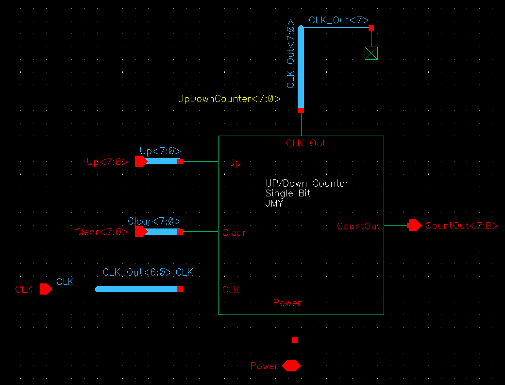
Figure 47:
This is the schematic of the 8-bit up/down counter using the single bit counter instantiated 8 times for 8-bits.
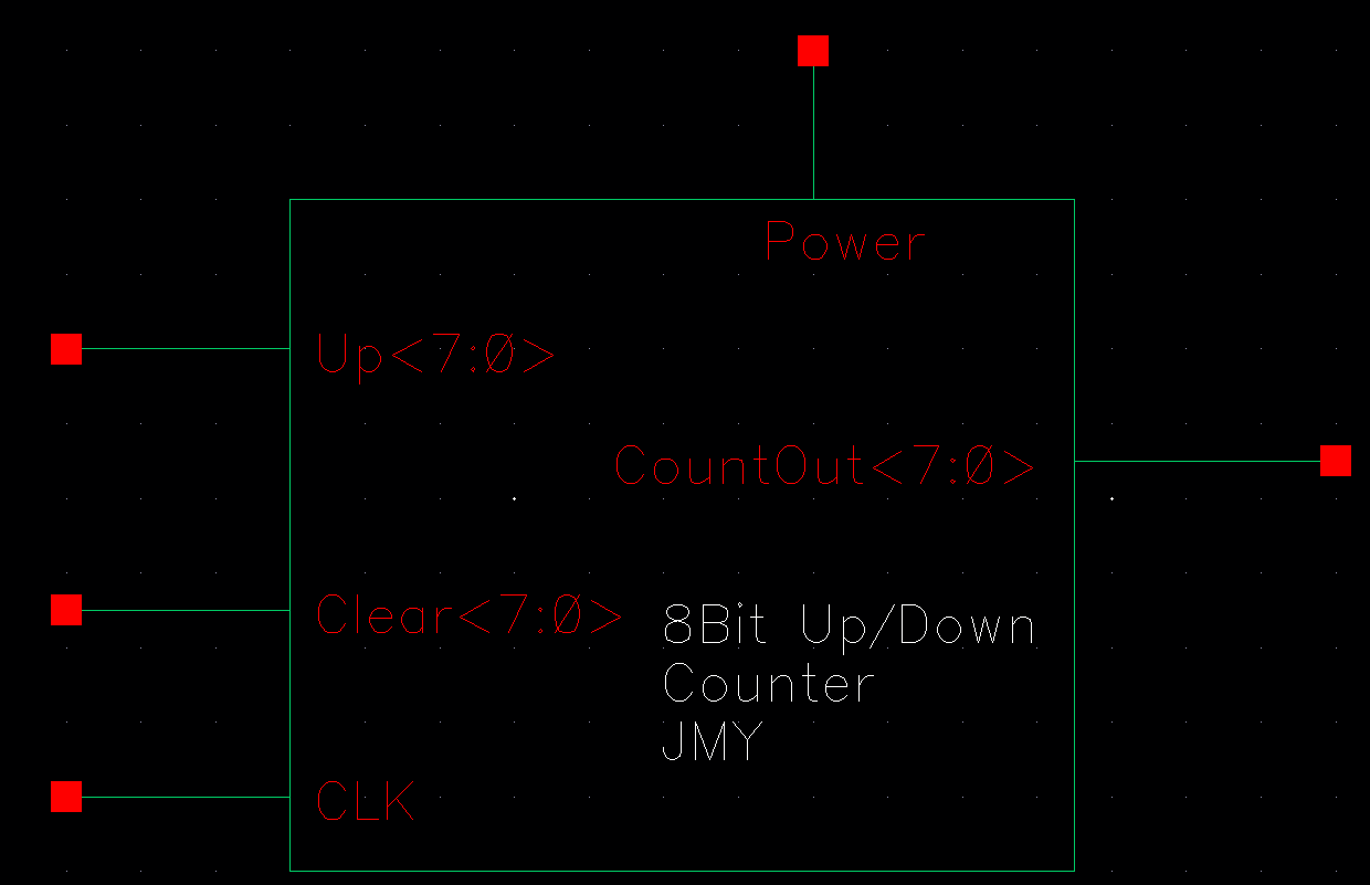
Figure 48:
This is the symbol created for an 8-bit up/down counter.
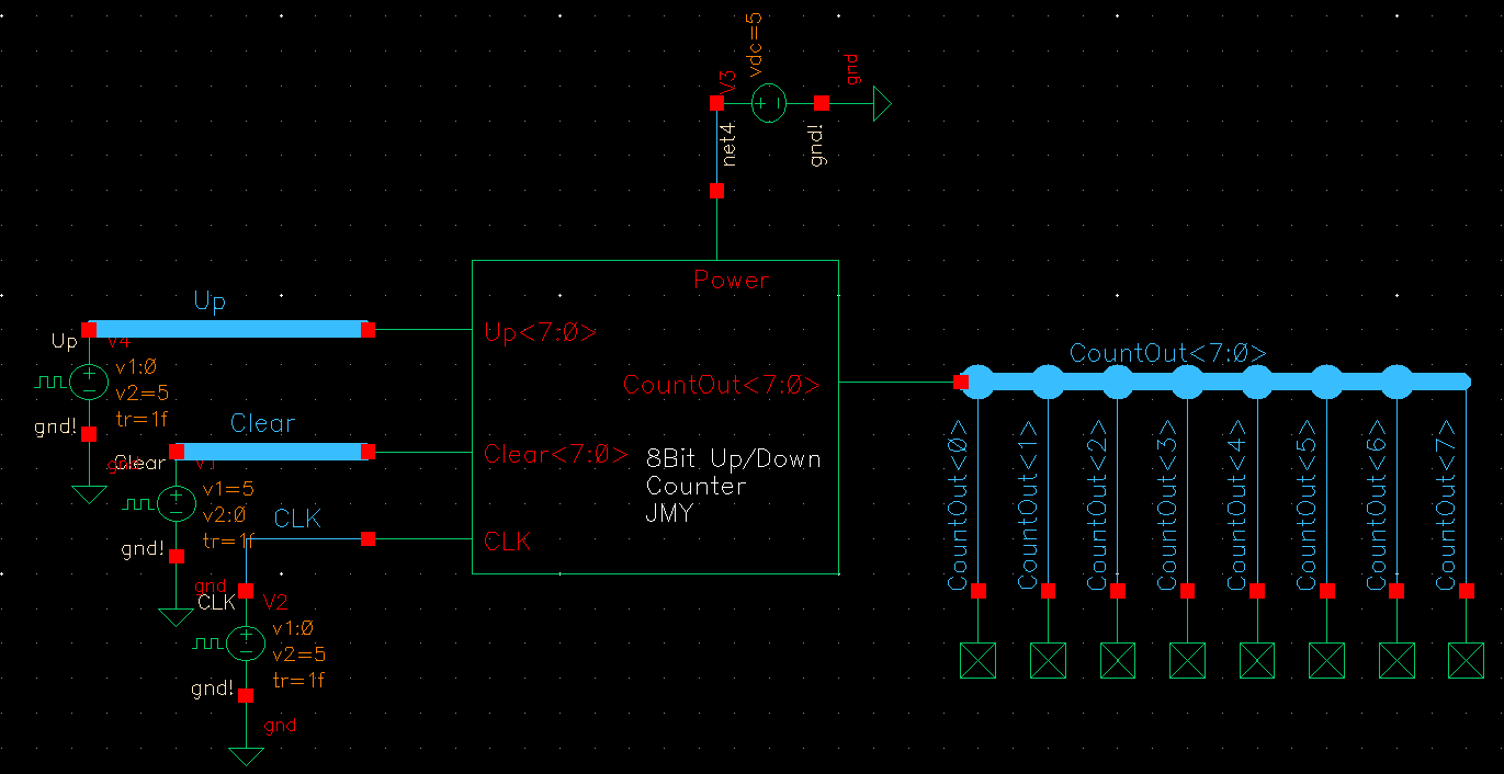
Figure 49:
This is the simulation schematic, used for verification of the 8-bit up/down counter and all its functionality.
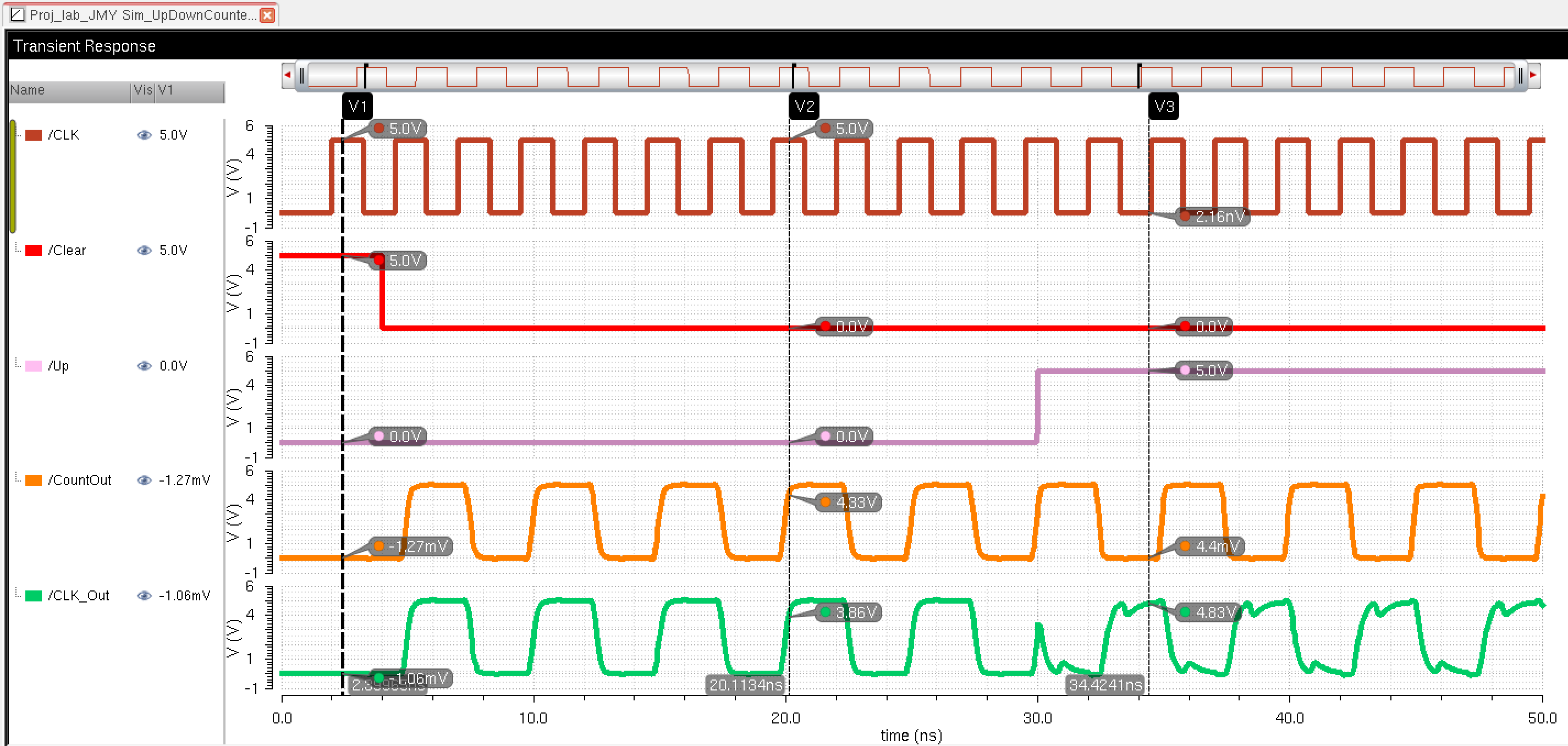
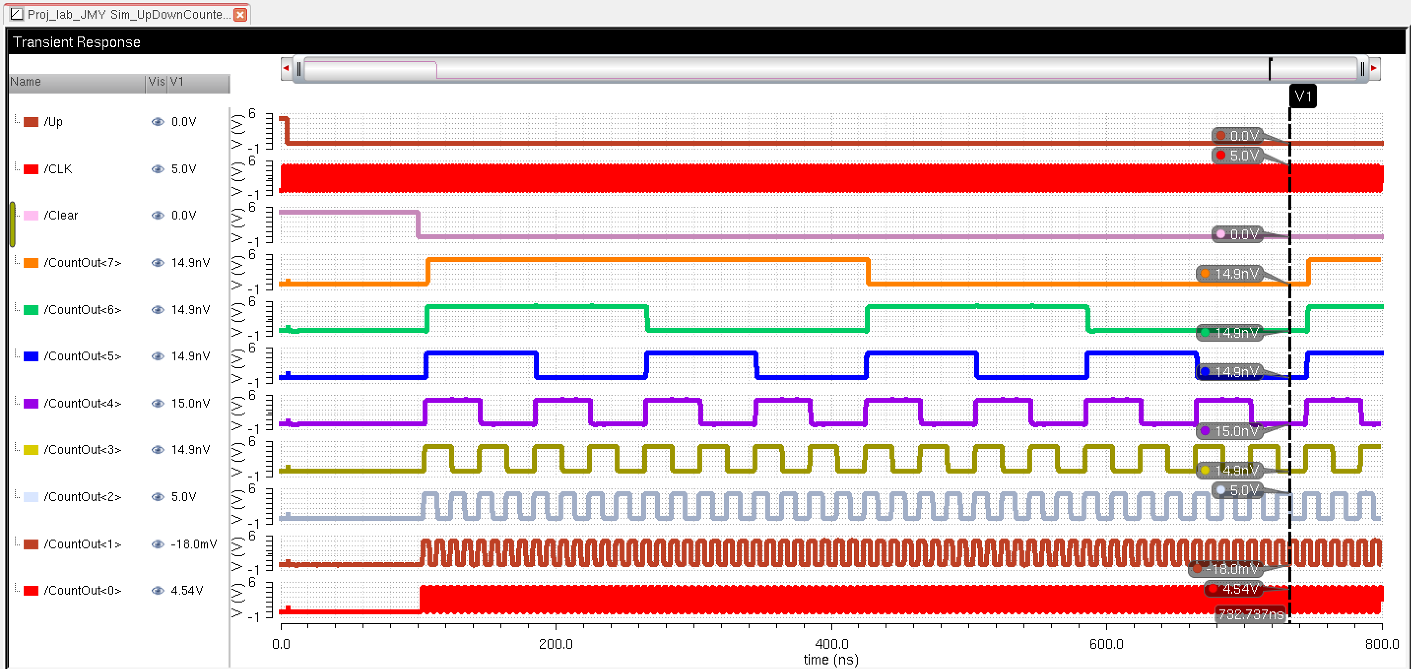
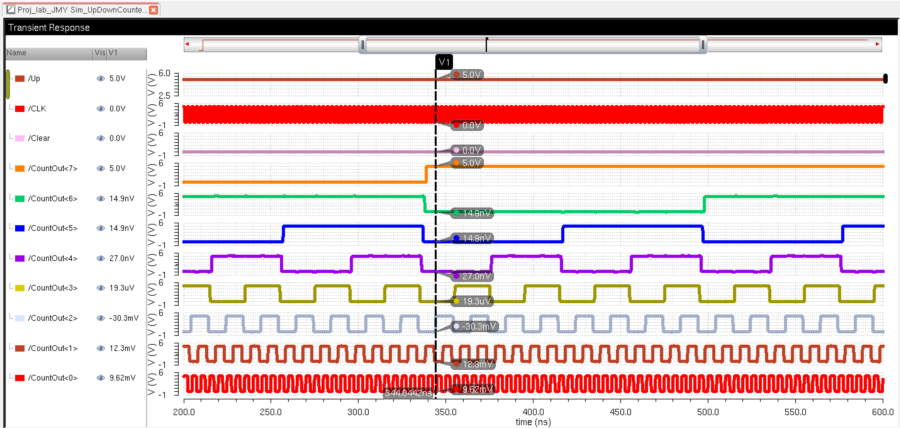
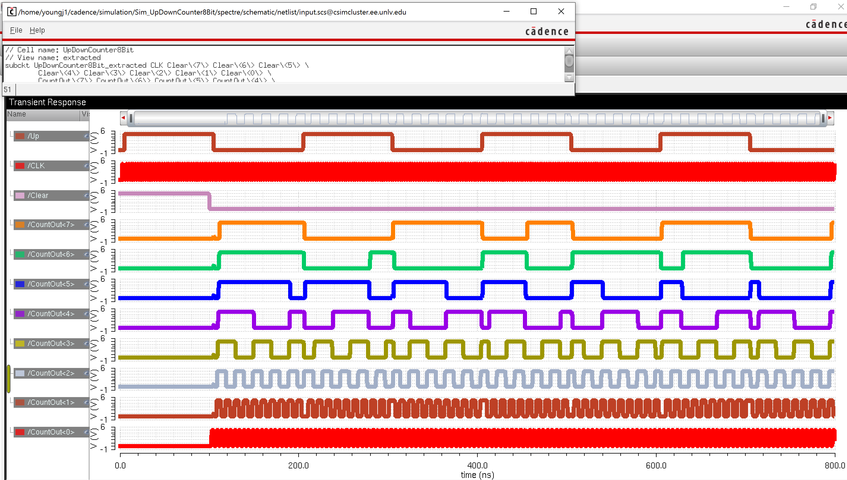
Figure 50:
These are the simulation results from figure , which show the down counter functionality of the up/down counter. Note: At V1 that all the output lines are zero and thus the down counter worked satisfactorily.
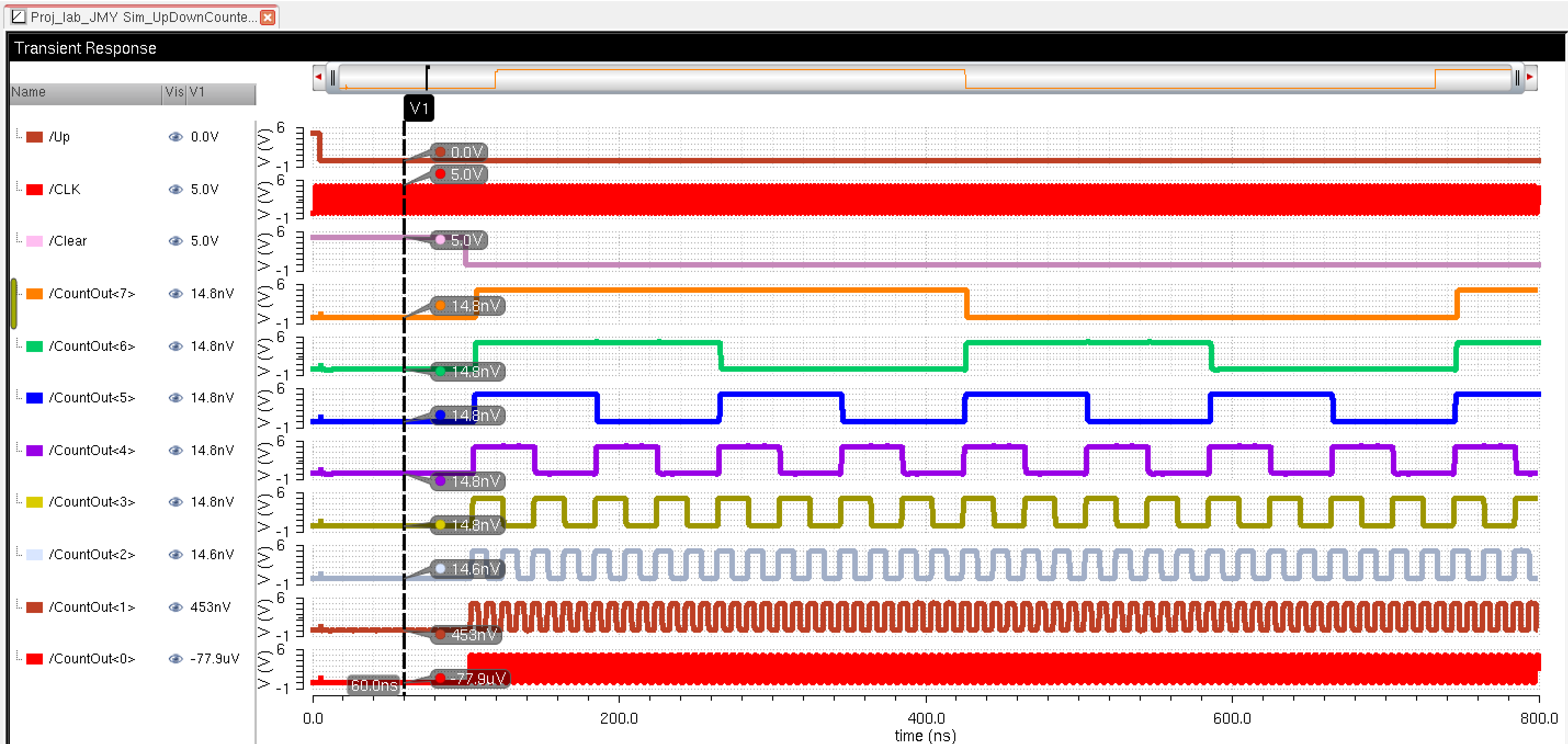
Figure 51:
This simulation shows the up functionality of the up/down counter. Note: V1 shows the 8th bit being high while the other are low and continues counting until all 8-bits are 1's. Another note, this is a zoomed in view of the simulation and thus the up signal is shown as on when it was initially off to produce delay.
Figure 52:
This simulation shows the active high clear in action, which resets all of the outputs to low for the up/down counter.
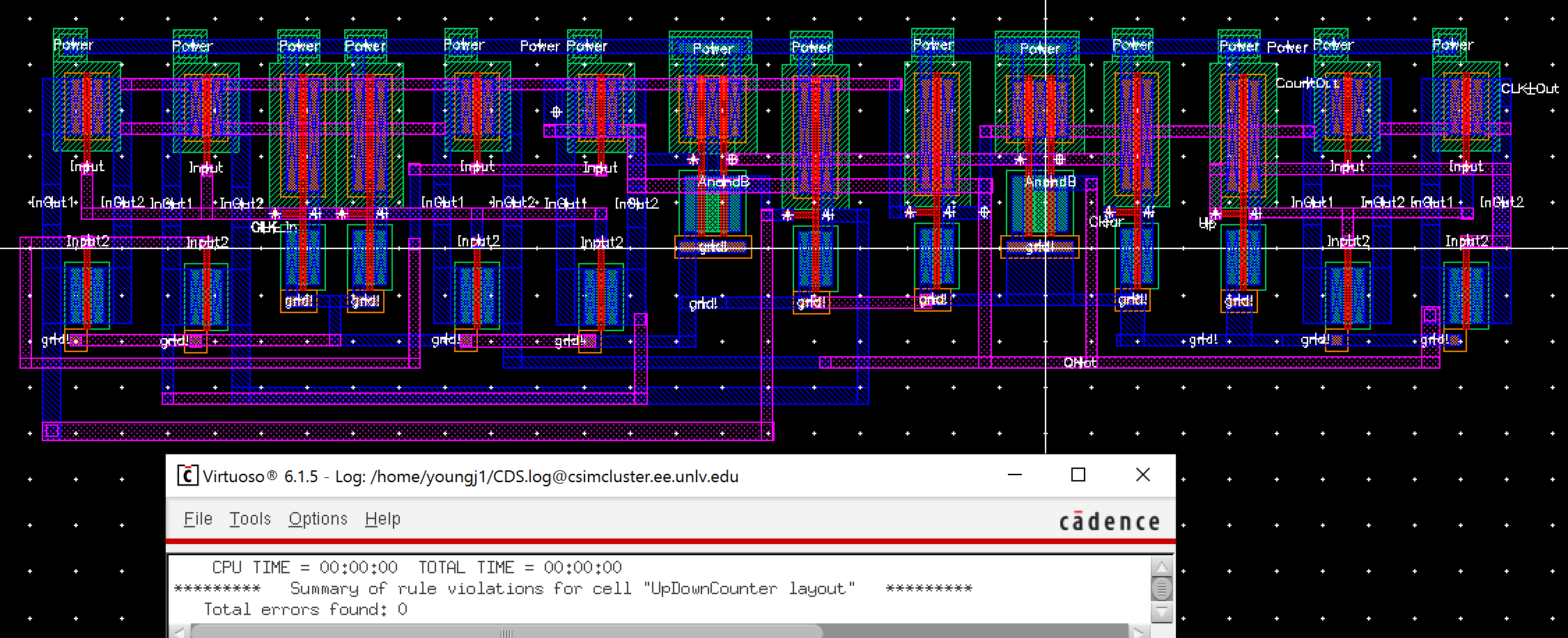
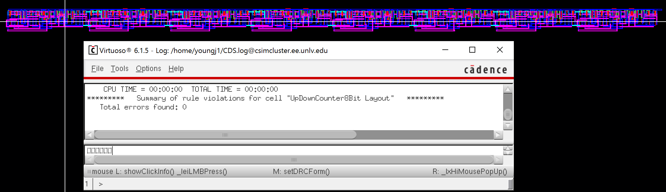
Layout 30:
This image is the layout of the up/down counter with a clear. It also shows that the layout DRCed without errors.
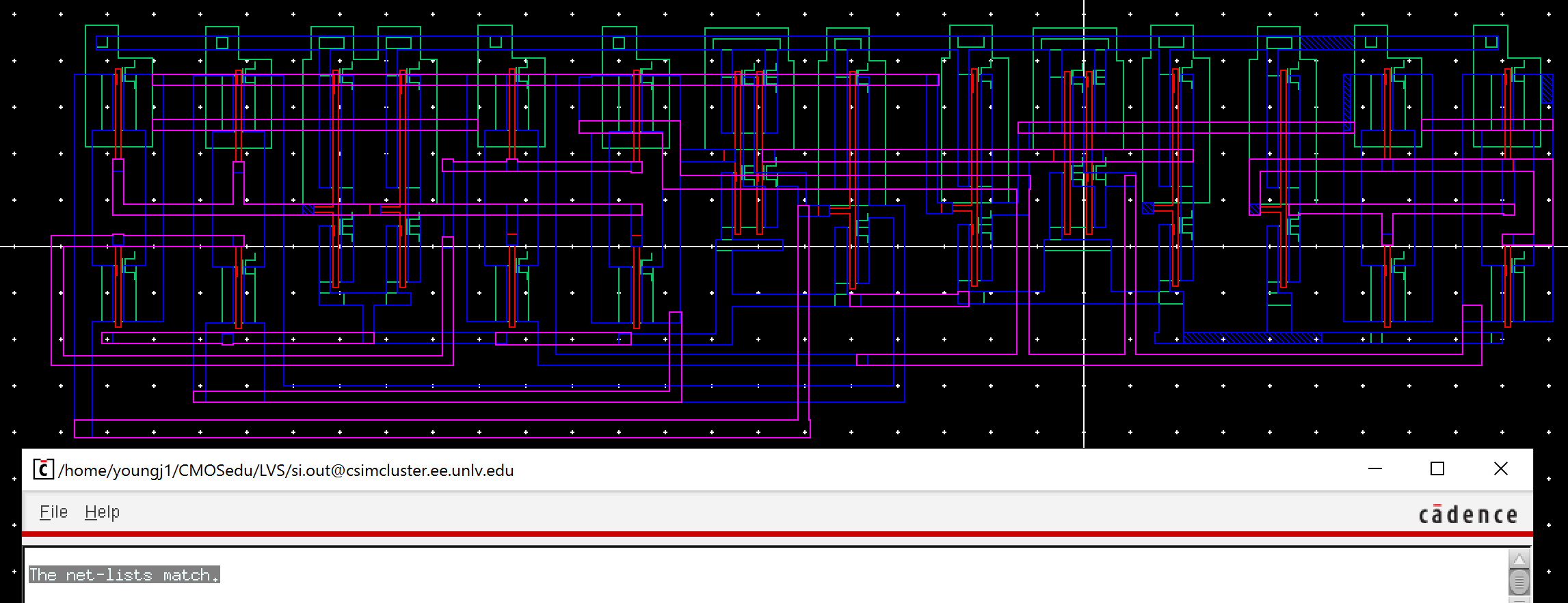
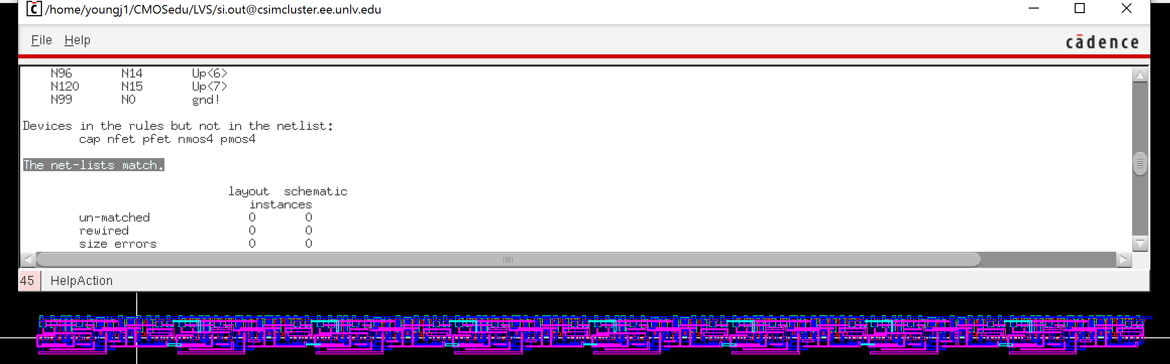
Layout 31:
This is the extracted layout of the up/down counter with a clear seen in Layout 30. It shows that LVS performed without errors.
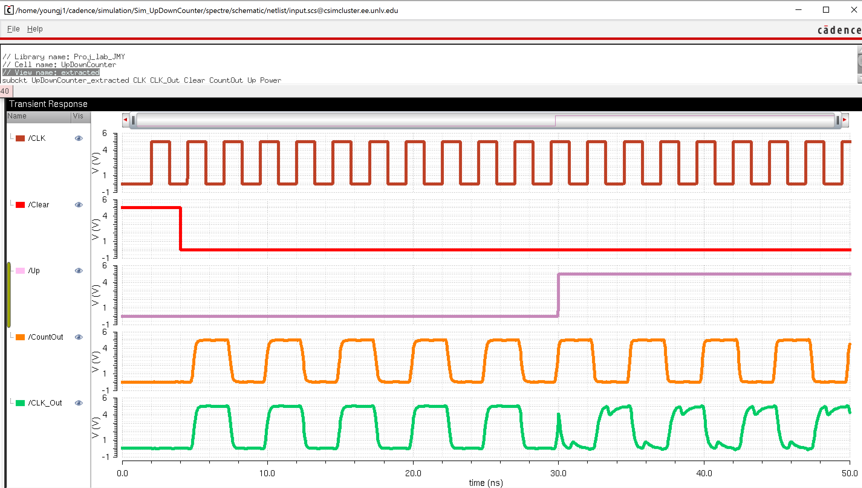
Layout 32:
This is an extracted simulation result using the layout of the circuit in Layout 31 to compare to the simulation of the schematic in Figure 50-52.
Voltage Divider:
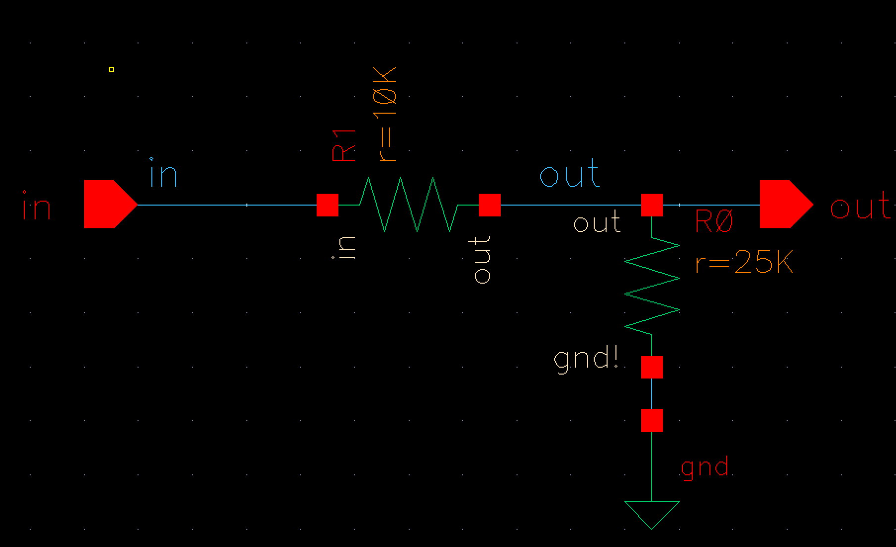
A voltage divider is used to scale an input voltage down to some desired level. A simple resistive divider comprises of two or more resistors connected in series to ground (common) with taps at the resistor junctions to pick off the desired voltage.
In this design a two resistor divider is used: a 10k resistor is connected in series with a 25k resistor connected to ground. Tapping the voltage at the junction of the two gives an output of: Vin (25k/(10k+25k)). For our example, Vin will be 5V and thus the output will be 3.57V.
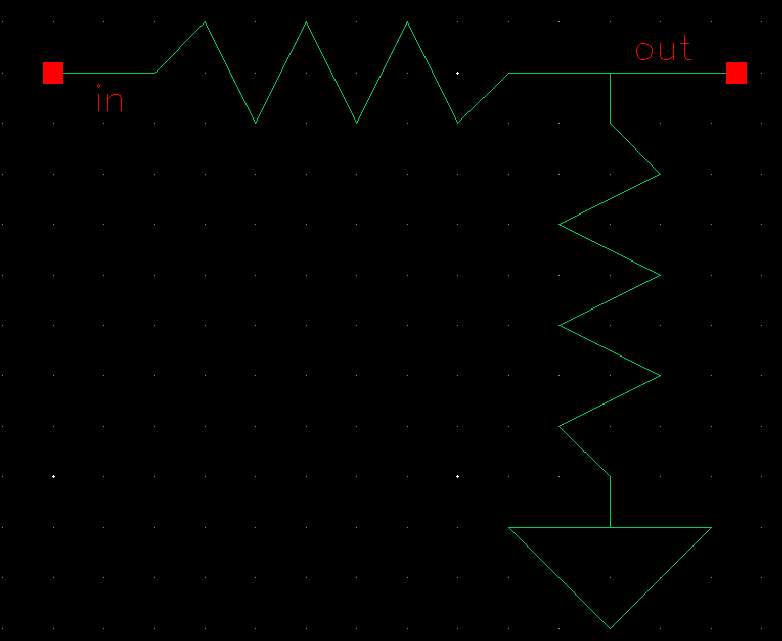
Figure 53:
This is the schematic of a voltage divider.
Figure 54:
This is a symbol created to show a voltage divider.
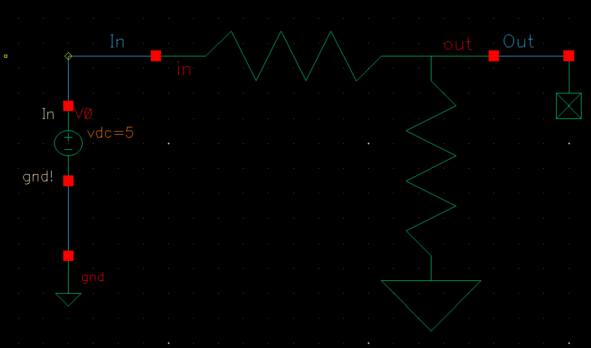
Figure 55:
This is the simulation schematic, used to verify that the output is as expected (as described above).
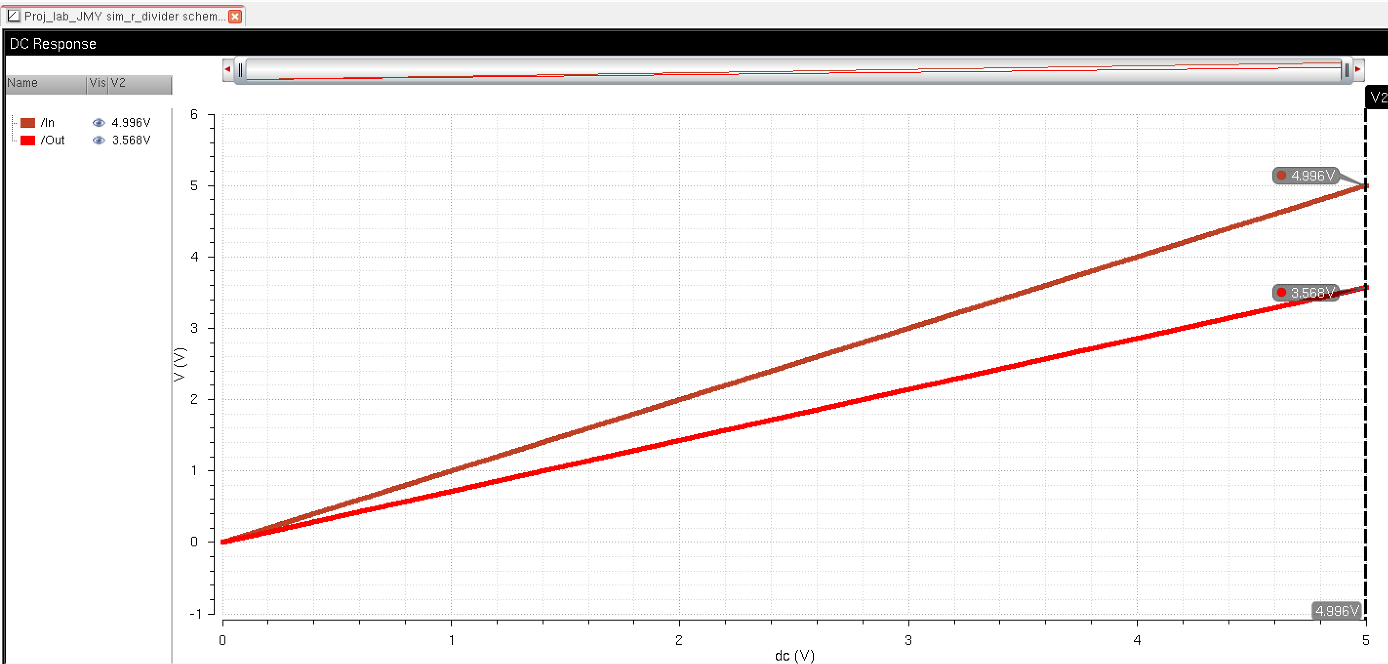
Figure 56:
These are the simulation results produced from the previous figure, showing how the ratio is maintained at various voltage levels. Note: When Vin is 5 volts, we get the expected 3.57V output.
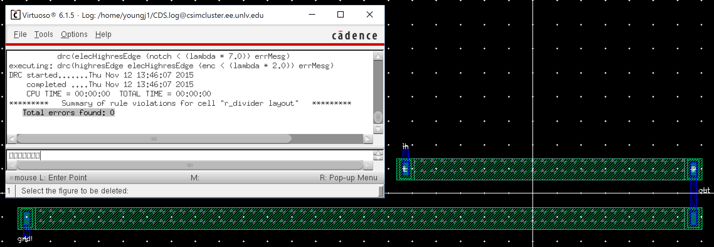
Layout 33:
This image is the layout of the voltage divider. It also shows that the layout DRCed without errors. Note: The 25k resistor is laid out in the n-well, as per project specifications. It was merged with the 10k resistor in n-well, not done as a separate instantiated layout. The actual 25k resistor is the same as seen here, which can be seen in the project folder below.
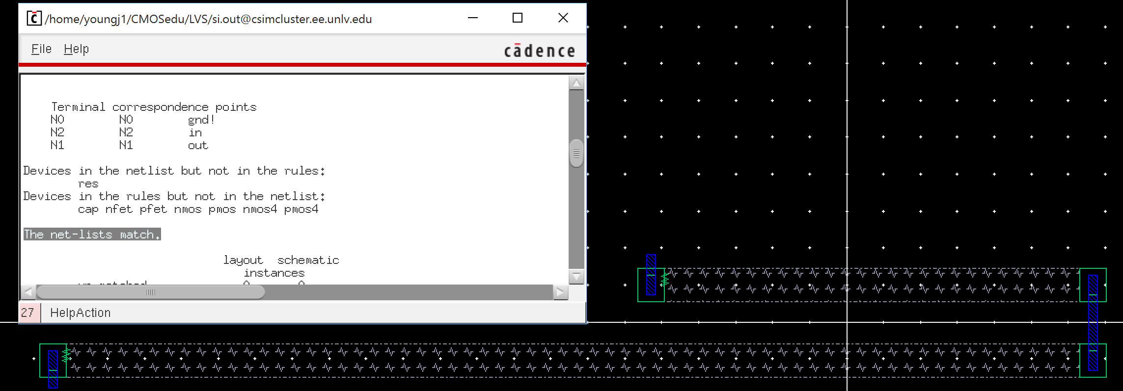
Layout 34:
This is the extracted layout of the voltage divider seen in Layout 33. It shows that LVS performed without errors.
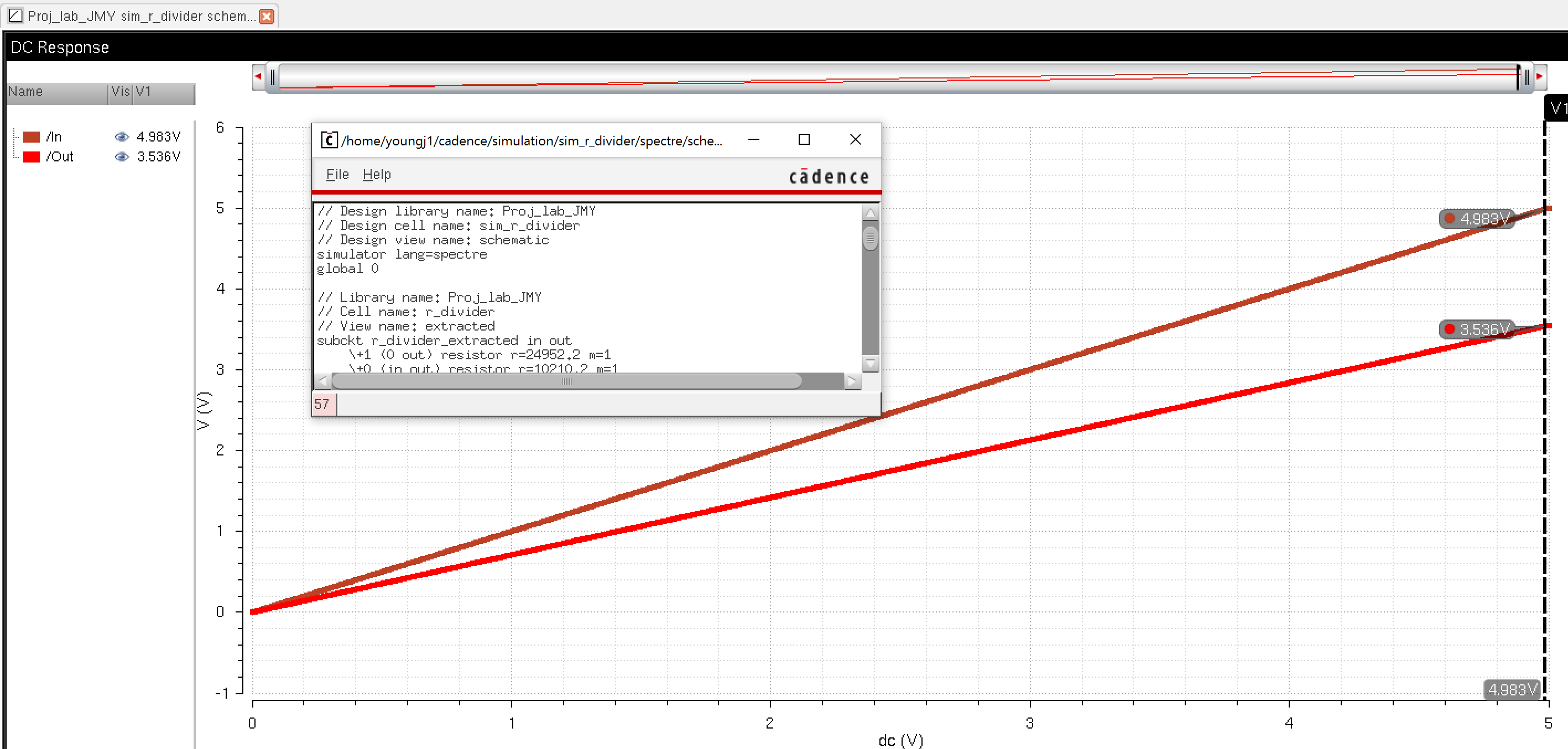
Layout 35:
This is an extracted simulation result using the layout of the circuit in Layout 34 to compare to the simulation of the schematic in Figure 56.
Back Up & Design Directory:
The lab directory containing the layouts, schematics, simulations, and symbols generated in this lab report can be downloaded by clicking this link: Proj_lab_JMY.zip. This link is provided for informational and grading purposes only. All other use is prohibited.