Lab 1 - EE 421L
Digital Integrated Circuit Design
Author:
Matthew Meza
Email:
mezam11@unlv.nevada.edu
August
31, 2015
Lab
Intro, Lab Report, Cadence
Pre-lab work
- The
lab reports will be drafted
using html and placed on CMOSedu.
- Prior
to the first day of lab,
but no earlier than one week before the lab starts, get a CMOSedu
account, using your UNLV email address, from Dr. Baker,
rjacobbaker@gmail.com
- Review
the material seen here covering editing webpages (do
this before the first lab)
Lab Description
- This
first lab will go through the first part of Tutorial 1 seen here.
- Use an Xterm
(written and video)
as discussed in class NOT a remote
desktop as used in the tutorials.
Lab Requirements
- Go
through Tutorial 1 up to the 25th image in the tutorial.
-
Simply showing
some of the images in this tutorial (that you generated) with some
simple coherent narrative
-
Discuss how you
will do regular backups while working on the future labs by zipping up
your work and emailing it to yourself or uploading to dropbox, google
drive, etc. with file names including the date (include at least two
images to support your discussion).
Tutorial
Images
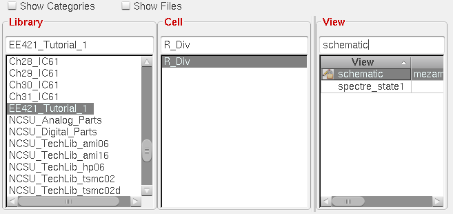
In order to create a
schematic for simulation a Library must be made
followed by a Cell.
Cadence has a very heirarchal
system which helps keep projects
organized.
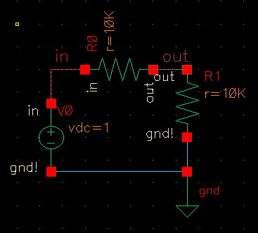
Shown below is the resistive
voltage divider schematic. Notice
that the two nodes (nets)
labeled "in" and "out" are
highlighted. This means that they are chosen
to be plotted in
the transient simulation. The
voltage source, ground, and resistors
were introduced into
the schematic by pressing "i"
(instance) and selecting parts from the
NCSU_Analog_Parts
folder.
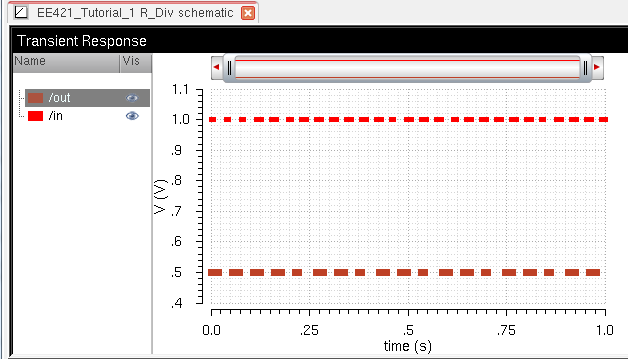
The image below shows the
transient response of the resistive voltage
divider circuit shown above.
The voltage divider uses two
10K resistors which halfs the voltage.
When simulating and plotting curves,
the line thickness can be
adjusted by right clicking on the name (such
as /out or /in) and clicking trace
properties. This is helpful
if a snapshot of the curve must be taken
for others to view.
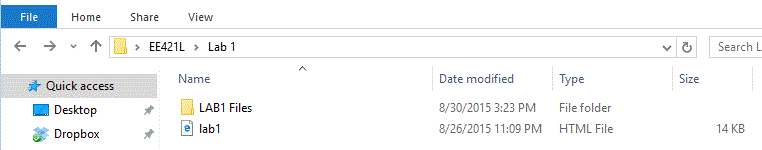
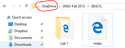
Backup
All of my work done in EE421
Lab will be backed up via Onedrive.
Onedrive will allow me to access
my work from my laptop and
any other school computer if necessary. The
image below shows the lab work
saved on my personal computer.
The image bleow shows the
work being backed into Onedrive!
Return
to EE 421 Labs