EE 421L Digital Integrated Circuit Design
Laboratory - Lab 7
11/16/16
Using buses
and arrays in the design of word inverters, muxes,
and high-speed adders
Pre-lab
work
o
Back-up all of your work from the
lab and the course.
o
Go through Tutorial 5
o
Read through the entire lab
before starting it.
Experiment
1
Wide
wires (buses) are added using the bindkey shift+W or the menu button seen circled below.
Arrayed
symbols (by changing the symbol's name) are used to make schematics
concise and easier to use.

Examine the circuit used for inverting a 4-bit word seen below
left. The inverter uses 6u/0.6u NMOS and PMOS devices.
We can make an equivalent, more concise, schematic by
instantiating an inverter and naming the inverter using an arrayed name
(I0<3:0> see image below right). Connect a wide-wire (bus) as seen
below and connect it to input and output pins. Name the pins as seen
below. This schematic is equivalent to the one seen to the left but
obviously more concise. For your lab report please use cell names that
indicate the current semester and your initials.


Create
a symbol for the schematic as displayed below left. Using this symbol create
a simulation schematic like the one seen below right.
o All four inverters' inputs are
tied together to an input pulse source.
o The out<0> is not
connected to a load while out<3> is connected to a 100fF load.
o The out<1> is connected to
a 1 pF load while out<2> is connected to a 500 fF
load.


Show,
in your lab report, how a capacitive load influences the delay and rise/fall
times.
The first experiment required
drafting the schematic and symbol for a 4-bit inverter using buses and arrays.
The schematic with DRC verification is displayed below to the left and the
corresponding symbol is displayed below to the right. Note the symbol naming
convention is followed with the X4
indicating a 4-bit inverter. The files used for this experiment are located in inv_4bit_EM_f16. The inverter schematic
with NMOS and PMOS symbols was initially created and can be viewed in Lab5.


Next, a schematic connected to the
loads as directed in the laboratory instructions was created and simulated. The
schematic with DRC verification is displayed below. The following schematic can
be found in the file sim_inv_4bit_EM_f16.

The ADE-L simulation results for all three
loads are displayed below. As seen below, the size of the capacitive load
influences the rise and fall times due to the delay inherent in each load. For
example, the delay for the 100fF load is smaller than the delay for the 1pF
load. Similarly, the 500fF load has a higher delay than the 100fF load, but a
smaller delay than the 1pF load. These results verify the intuitive expectation
that a larger capacitive load will have a longer delay than smaller capacitive
loads. The inverter is unable to supply enough current to drive the higher
capacitive loads as easily as the smaller loads, thus the ouputs
of the larger loads do not approximate the input signal as well as the smaller
loads.

Experiment
2
Create
schematics and symbols for an 8-bit input/output array of the following gates:
o Inverter
o NAND
o NOR
o AND
o OR
Provide
a few simulation examples using these gates.
The first gate created was the 8-bit inverter.
The schematic and symbol, both with DRC verification, are displayed below to
the left and right, respectively. Note again, naming conventions are followed.
The files below are found in inv_8bit_EM_f16.


Next, a schematic
for simulation of the 8-bit inverter was created. The schematic with DRC verification
is displayed below to the left. The simulation results demonstrating the 8-bit
inverter functions properly is displayed to the right. The related file is
titled sim_inv_8bit_EM_f16. Note the inverter functions as intended, going high
when the input is low and going low when the input is high. The capacitive
loads were not included in the following simulations simply due to the
comprehension these would result in similar delays as seen in the 4-bit
inverter and because the laboratory instruction did not specifically mandate
the capacitive loads to be included in simulation of these gates. This was not
an optimal choice, but due to the loss of access to the Cadence software for an
extended period, tradeoffs were required to allow completion of all coursework
within the alotted timeframe.


The next gate
created was the 8-bit NAND gate. The schematic and symbol, both with DRC
verification, are seen below to the left and right, respectively. These files
are found in NAND_8bit_EM_f16.


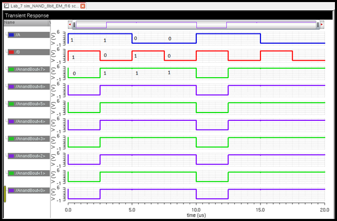
Continuing, a
schematic for simulating the 8-bit NAND gate was designed. The schematic with
DRC verification is displayed below to the left. The simulation results,
displayed below to the right, demonstrate the NAND gate functions as intended.
The files below can be found in sim_NAND_8bit_EM_f16.
The NAND gate schematic displaying NMOS and PMOS symbols can be seen in Lab6.

The truth table for
a 2-input NAND is included as a reference to verify the above simulation
results. Each output can be considered AnandB for simplification.
|
A |
B |
AnandB |
|
0 |
0 |
1 |
|
0 |
1 |
1 |
|
1 |
0 |
1 |
|
1 |
1 |
0 |
Following the NAND,
an 8-bit NOR gate was designed. The schematic and symbol, both with DRC verification,
are seen below to the left and right, respectively. These files are found in NOR_8bit_EM_f16.


For reference, the basic NOR schematic
displaying NMOS and PMOS symbols is displayed below.

Following, a schematic
for simulating the 8-bit NOR gate was drafted. The schematic with DRC
verification is displayed below to the left. The simulation results, displayed
below to the right, demonstrate the NOR gate functions as intended. The files
below can be found in sim_NOR_8bit_EM_f16.


The truth table for
a 2-input NOR is included as a reference to verify the above simulation
results. Each output can be considered AnorB for simplification.
|
A |
B |
|
|
0 |
0 |
1 |
|
0 |
1 |
0 |
|
1 |
0 |
0 |
|
1 |
1 |
0 |
The next gate
designed was an 8-bit AND gate. The AND gate is simply the NAND gate with an
inverter added to the output. The AND gate schematic displaying NMOS and PMOS
symbols is displayed below for reference.

The AND gate schematic
and symbol, both with DRC verification, are seen below to the left and right,
respectively. These files are found in AND_8bit_EM_f16.


Next, a schematic
for simulating the 8-bit AND gate was drafted. The schematic with DRC
verification is displayed below to the left. The simulation results, displayed
below to the right, demonstrate the AND gate functions as intended. The files
below can be found in sim_AND_8bit_EM_f16.


The truth table for
a 2-input AND gate is included as a reference to verify the above simulation
results. Each output can be considered AandB for simplification.
|
A |
B |
AandB |
|
0 |
0 |
0 |
|
0 |
1 |
0 |
|
1 |
0 |
0 |
|
1 |
1 |
1 |
The next gate
designed was an 8-bit OR gate. The OR gate is simply the NOR gate with an
inverter added to the output. The OR gate schematic displaying NMOS and PMOS
symbols is displayed below for reference.

The OR gate
schematic and symbol, both with DRC verification, are seen below to the left
and right, respectively. These files are found in OR_8bit_EM_f16.


Next, a schematic
for simulating the 8-bit OR gate was drafted. The schematic with DRC
verification is displayed below to the left. The simulation results, displayed
below to the right, demonstrate the OR gate functions as intended. The files
below can be found in sim_OR_8bit_EM_f16.


The truth table for
a 2-input OR gate is included as a reference to verify the above simulation
results. Each output can be considered AorB for simplification.
|
A |
B |
AorB |
|
0 |
0 |
0 |
|
0 |
1 |
1 |
|
1 |
0 |
1 |
|
1 |
1 |
1 |
Experiment
3
Examine
the following schematic. This is the schematic of a 2-to-1 DEMUX/MUX (and the
symbol).
o Simulate the operation of this
circuit using Spectre and explain how it works.
o Make sure to show, using
simulations, how the circuit can be used for both multiplexing and
de-multiplexing.


The first part of Experiment 3
involved simulating the 2-to-1 DEMUX/MUX. First, a 2-to1 DEMUX/MUX schematic
and symbol were designed and DRC verified. These are displayed below to the
left and right, respectively. These files can be found in the file MUX_2_1_EM_f16.


Next, the 2-to-1 DEMUX/MUX simulation
schematic with DRC verification is displayed below to the left. The simulation
results are displayed to the right. These files can be found in simMUX_2_1_EM_f16.


The 2-to-1 MUX has a control signal,
a 'Select' input, denoted 'S', and a 'Select Inverse' input, denoted 'Sinv'. The circuit output, denoted 'Z', is defined by the
equation 'Z = A*S + B*Sinv'. The way this circuit
works is the output 'Z' will either replicate the signal coming in from the
input 'A' if 'S' is high and 'Sinv' is low or 'Z'
will replicate the signal coming in from the input 'B' if 'Sinv'
is high and 'S' is low. Thus, the MUX can be viewed as a switch that determines
the output. This circuit uses an inverter to implement 'Sinv'
and transmission gates (TG) that pass either input A or input B to the output.
The TG for the A input has 'Sinv' connected to the
PMOS and 'S' connected to the NMOS, thus allowing A to pass if 'S' is high.
Conversely, the TG for the B input has 'S' connected to the PMOS and 'Sinv' connected to the NMOS, thus holding B from passing
when 'S' is high and passing B when 'S' is low. This can be seen on the plot
above. The first interval has A low, B low, 'S' low, and 'Sinv'
high. Since 'Sinv' is high, the output 'Z' mirrors B,
thus the output is low. The only change in the next interval is B is high, thus
the output Z is also high.
To implement the 2-to-1 MUX as a
DEMUX, the multiple input lines of the MUX are converted to output lines and
the output of the MUX is converted to an input line. The input signal 'Z' is
controlled by 'S' such that when 'S' is high, output 'A' passes the signal 'Z'
and when 'S' is low, output 'B' passes 'Z'. The DEMUX simulation schematic and
results are displayed below to the left and right, respectively. The DEMUX was
created by changing the MUX pins A, B, and Z to input/output pins. These files
can be found in sim_DEMUX_2_1_EM_f16.
Note, the DEMUX operates as intended, passing the
signal A when S is high and passing B when Sinv is
high.


Create
an 8-bit wide word 2-to-1 DEMUX/MUX schematic and symbol. Include an inverter
in your design so the cell only needs one select input, S (the complement, Si,
is generated using an inverter). Use simulations to verify the operation of
your design.
Using the cell above, an 8-bit 2-to-1
DEMUX/MUX was designed and simulated. The schematic with DRC verification is
displayed below to the left and the symbol is displayed below to the right.
Note the inverter added to the design so there is only one select input. These
files can be found in the file MUX_2_1_8bit_EM_f16.


Following, the 8-bit 2-to-1 DEMUX/MUX
was simulated with the simulation schematic displayed to the left and the
simulation results displayed below to the right. Note the outputs match the
output for the previous design, however there is no output for 'Sinv'. These files can be found in the file sim_MUX_2_1_8bit_EM_f16.


Experiment
4
Finally,
draft the schematic of the full-adder seen in Fig. 12.20 using 6u/0.6u devices
(both PMOS and NMOS).
o Create an adder symbol for
this circuit (see the symbol used in lab6). Use this symbol to draft an 8-bit
adder schematic and symbol.
For how to label the bus so the carry out of one full-adder goes to the carry
in of another full-adder review the ring oscillator schematic discussed in
Cadence Tutorial 5.
Simulate
the operation of your 8-bit adder.
First, the Full-Adder (FA) schematic
was built using 6u/0.6u devices. The schematic with DRC verification is
displayed below. These files can be found in FA_EM_f16.

Next, the symbol for the FA was
created as displayed below.

To ensure proper logic functioning,
the FA was simulated. The simulation schematic and results are displayed below
to the left and right respectively. These files can be found in sim_FA_EM_f16.


The truth table for
a FA is included as a reference to verify the above simulation results.
|
A |
B |
Cn (Cin) |
Cn_1 (Cout) |
Sn |
|
0 |
0 |
0 |
0 |
0 |
|
0 |
0 |
1 |
0 |
1 |
|
0 |
1 |
0 |
0 |
1 |
|
0 |
1 |
1 |
1 |
0 |
|
1 |
0 |
0 |
0 |
1 |
|
1 |
0 |
1 |
1 |
0 |
|
1 |
1 |
0 |
1 |
0 |
|
1 |
1 |
1 |
1 |
1 |
Following the above simulation, the
concise 8-bit FA schematic and symbol were drafted. The schematic with DRC verification
is displayed below to the left and the symbol is displayed below to the right.
These files can be found in FA_8bit_EM_f16.


Next, the 8-bit FA simulation
schematic displayed below was drafted. The schematic and spectre
files can be found in sim_FA_8bit_EM_f16

Following, the 8-bit FA simulation
results are displayed below. Note the results below match the excitation table
above.

Lay
out this 8-bit adder cell (*note* that this is the only layout required in this
lab).
Show that your layout DRCs and LVSs correctly.
The 8-bit FA layout was drafted by
first laying out a single bit FA. The layout with DRC verification and
extracted view with LVS verification are displayed directly below. These files
are found in FA_EM_f16.

Next, the DRC verification.

The extracted view with LVS follows.

After LVS verification of the 1-bit
FA extracted view, the 8-bit FA layout, displayed below with DRC verification,
was completed. These files are found in FA_8bit_EM_f16.

Finally, the 8-bit FA layout was
extracted and LVS verification was completed. The results are displayed below.

To ensure the 8-bit layout was
drafted correctly, the extracted view was simulated to compare the output to
the simulation performed earlier with the schematic and 8-bit FA symbol. Recall
the extracted view can be simulated by changing the ADE-L Setup > Environment
as previously seen in Lab
3. The simulation results are displayed below along with the netlist verifying
the extracted view was used for the simulation. Note the simulation results for
the extracted view identically match the schematic view simulation results.

The netlist demonstrating the
extracted view was used for the simulation results above. This concludes the
experiments required for Lab 7.

Conclusion
Laboratory 7 provided experience using
buses and arrays to create organized schematics of 8-bit logic gates, including
an inverter, a nand gate, a nor gate, an and gate and
an or gate. Additionally, these gates were all simulated to verify proper
design and operation. The experiments also included the drafting and simulation
of a 2-to-1 MUX/DEMUX to provide clarity on the operation of these logic
circuits. Lastly, an 8-bit Full-Adder was designed and simulated, including a
layout view with successful DRC and LVS verifications.
Return to
Monahan Lab Report Directory
Return to EE 421L
Fall 2016 Student Directory