EE 421L Digital Integrated Circuit Design Laboratory - Lab
5
10/5/16
Pre-lab
work
o Back-up all of your work from
the lab and the course.
o Go through Tutorial
3
Experiment
Draft
schematics, layouts, and symbols for two inverters having sizes of:
o 12u/6u (= width of the PMOS /
width of the NMOS with both devices having minimum lengths of 0.6u)
o 48u/24u where the devices use
a multiplier, M = 4 (set along with the width and length of the MOSFET
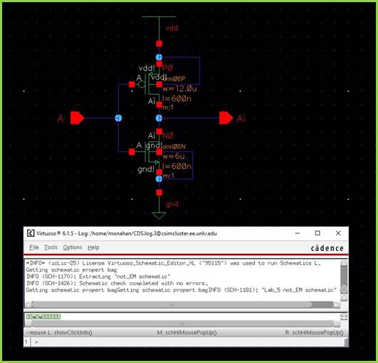
The
first inverter designed was the 12u/6u inverter with minimum length of 600n.
The associated file is titled not_EM. The designs were drafted using the NCSU Tech Library
and instantiated pmos and nmos
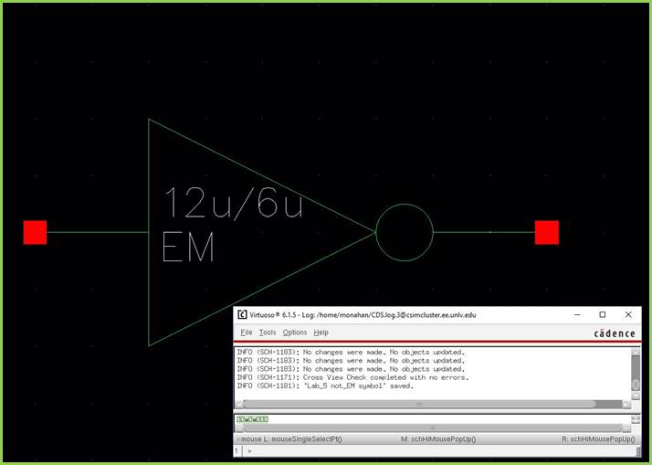
devices. The inverter schematic with DRC verification is displayed to the left
below. The inverter symbol with DRC verification is displayed to the right
below. Note, the schematic displays two pins, input A, and output Ai. The
symbol view reflects the widths of the PMOS and NMOS for ease of reference.
Next,
the 12u/6u inverter layout and extracted layout were created. The layout with
DRC verification is displayed to the left below and the extracted layout with
LVS verification is displayed to the right below. Note the power in the layout
is connected to the n-well via the ntap cell and
there are four pins, input A, output Ai, input-output vdd!, and input-output gnd!.


After
finishing the first inverter, the 48u/24u inverter with multiplier M=4 was
created following the same basic procedure. The associated file is titled not_4_EM. The schematic, below left with
DRC verification, and the symbol, below right with DRC verification, were
created first. Note the multiplier, m=4, is visible on the schematic view.


Following
format, the 48u/24u layout and extracted layout were designed with successful
DRC and LVS verifications. The layout is displayed directly below.

Next,
the extracted view with successful LVS verification is displayed below.

The
only experienced difficulty in this portion of the lab was laying out the
metal1 connections for the 48u/24u inverter design. Specifically, connecting
the devices properly the first attempt required referencing the CMOS textbook
and then the supplied Lab 5 design files to validate the proper technique for
the metal 1 connections was followed. After
referencing these resources, the 12u/6u and 48u/24u inverter schematics,
symbols and layouts were finished, thus concluding the first requirement for
Laboratory 5.
Using
SPICE simulate the operation of both of your inverters showing each driving a
100 fF, 1 pF, 10 pF, and 100 pF capacitive load
o Comment, in
your report, on the results
Use UltraSim
(Cadence's fast SPICE simulator for larger circuits at the cost of accuracy)
and repeat the above simulations
o Use Setup
-> Simulator/Directory/Host and select UltraSim as
seen below
o You'll also
have to point to the MOSFET models again as seen below
o Note that UltraSim only performs transient simulations (not AC,
Noise, DC, operating point, etc.)
o
Not
knowing this last item will lead to wasted time if trying to use UltraSim exclusively for simulations
Following the design of the
inverters, each inverter was simulated driving the specified 100fF, 1pF, 10pF
and 100pF capacitive loads. The associated file is titled sim_not_EM. The first step
required drafting a schematic to simulate using the inverter designs. To start,
the 12u/6u inverter was simulated. Notice the schematic view displayed below
shows 'Cload' for the capacitor value. This was done
to demonstrate the creation of a single schematic where the capacitive load was
varied as required for each successive simulation. Also, notice the inclusion
of a global vdd source as necessary due to the PMOS
source connection to vdd in the inverter. The voltage
to the inverter is a pulse from 0V to 5V.

The simulations were first performed
following the same procedures as performed in previous laboratory experiments
using Cadence. These steps include launching the Analog Design Environment (ADE
L), including the model libraries for the NMOS and PMOS devices as done in Tutorial2
, and performing a transient simulation. Next, the simulations were repeated
using UltraSim. Ultra Sim is activated via the ADE
Setup > Simulator/Directory/Host and selecting UltraSim
from the Simulator dropdown. These steps are displayed in the two images below.


The simulation results are displayed
below for comparison. The capacitive load for each simulation is labeled on
each plot with the Spectre simulation results (blue
and red traces) on the left and the UltraSim results
(red and green traces) displayed on the right. Notice for the 100fF load plots
directly below, the output is inverted, as the design intended.


The
simulation results demonstrate that a larger capacitive load results in a
larger time constant, RC, and consequently, a longer time for the capacitor to
charge and discharge. Thus, the inverter characteristics disappear as the
capacitive load increases. The simulations above verify that a 12u/6u inverter
in On's C5 process loses the
ability to invert with loads larger than 1pF. The 10pF load shows the output
starts to resemble a triangle wave rather than an inverter. Also, note the UltraSim and Spectre results
appear identical.
The
next step was to repeat the same simulations performed above using the 48u/24u
inverter. The associated file is titled sim_not_4_EM.
The schematic view with successful DRC verification is displayed below.

Once
again the simulations were performed using both Spectre
and UltraSim with the required capacitive loads. The
results are displayed below with Spectre results
(blue and red traces) displayed to the left and UltraSim
results (red and green traces) displayed to the right.


Initially,
the larger inverter operates similarly to the smaller inverter. However, due to
the increased width the 48u/24u inverter can supply more current and drive
larger loads than the 12u/6u inverter. This can be seen in a comparison of the
10pF loads for each inverter. The 12u/6u inverter is displayed to the left
below and the 48u/24u inverter is displayed to the right. Clearly, the 48u/24u
inverter drives the larger load easier. For simplicity, only the Spectre
results are included in the comparison.

Conclusion
Laboratory
5 included drafting schematics, layouts, and symbols for both a 12u/6u inverter
and a 48u/24u inverter, both with a minimum length of 600n. All design specifications
were met with successful DRC and LVS verifications performed and recorded.
Additionally, both inverters were simulated driving varying capacitive loads
using both Spectre and UltraSim.
The results of the simulation demonstrate the wider 48u/24u inverter is capable
of driving larger capacitive loads than the 12u/6u inverter.
Return to
Monahan Lab Report Directory
Return to EE 421L
Fall 2016 Student Directory