Lab 7 - EE 421L
Authored
by Martin Jaime,
email: jaimem5 at the UNLV students domain
Date November 16
Pre-lab work:
- Back-up all of your work from the lab and the course.
- Go through Tutorial 5 seen here.
- Read through the entire lab before starting it.
Lab Report
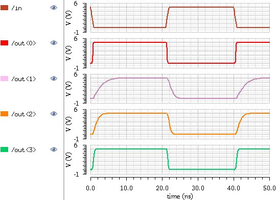
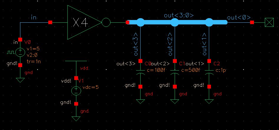
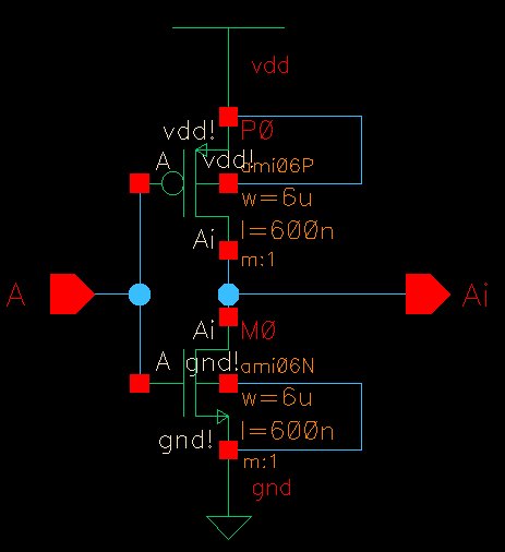
- Create an arrayed schematic of four inverters. Create its symbol and show simulations.
- Obviously, a capacitive load will cause a delay at the output that will increase with an increasing capacitance.
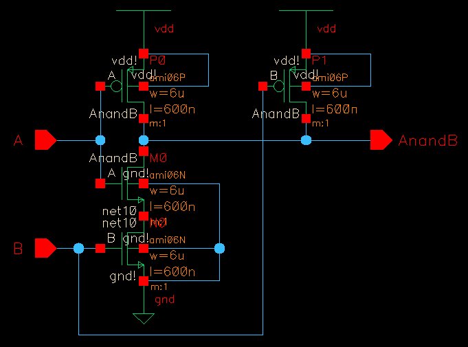
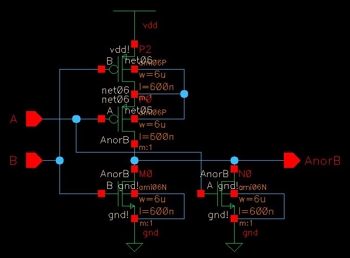
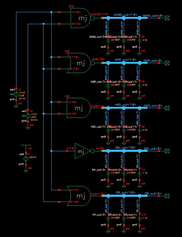
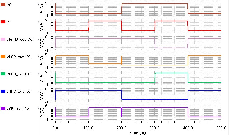
- Similaryly, create schematics and symbols for an 8-bit input/output array of: NAND, NOR, AND, inverter, and OR gates.
Provide a few simulation examples using these gates.
- Finally, draft the schematic of the full-adder seen in Fig. 12.20 using 6u/0.6u devices (both PMOS and NMOS).
Create an adder symbol for this circuit (see the symbol used in lab6).
Use this symbol to draft an 8-bit adder schematic and symbol.
For
how to label the bus so the carry out of one full-adder goes to the
carry in of another full-adder review the ring oscillator schematic
discussed in Cadence Tutorial 5.
Simulate the operation of your 8-bit adder.
Lay out this 8-bit adder cell (*note* that this is the only layout required in this lab).
Show that your layout DRCs and LVSs correctly.
The lab work can be found here: lab7.zip
All backed up work can be found at https://github.com/martinjaime/CMOSedu-Reports
EE421L Lab Student Listing | My Lab Directory | EE421 Home Page


