
Lab X - ECE 421L
Pre-lab work
Let's make a 10k n-well resistor layout after finishing the schematic part in Lab1. First, go to the menu Cell--> New Cell and enter the name and select the layout view seen below.
In the library tutorial_1, I create a group of cells including R_divider{lay} and R_divider{sch}. Then select the N-well resistor node in the components tab(click on the arrow head in the bottom left-hand side of the menu).

Use Ctril+I or Edit--> Properties--> Object Properties to set the size of the resistor as above, L=187.5 W=15 and a resistance of 10k.
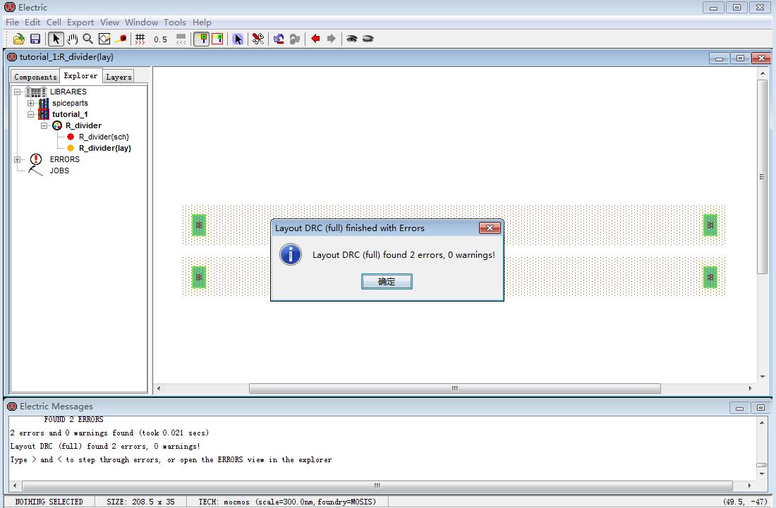
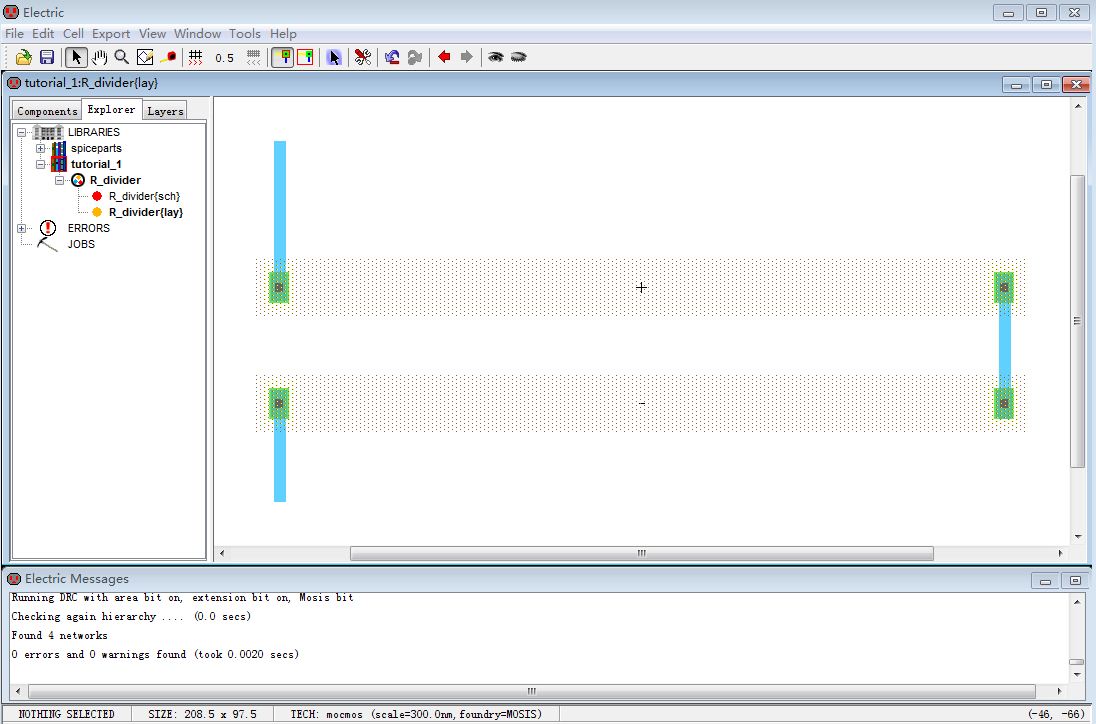
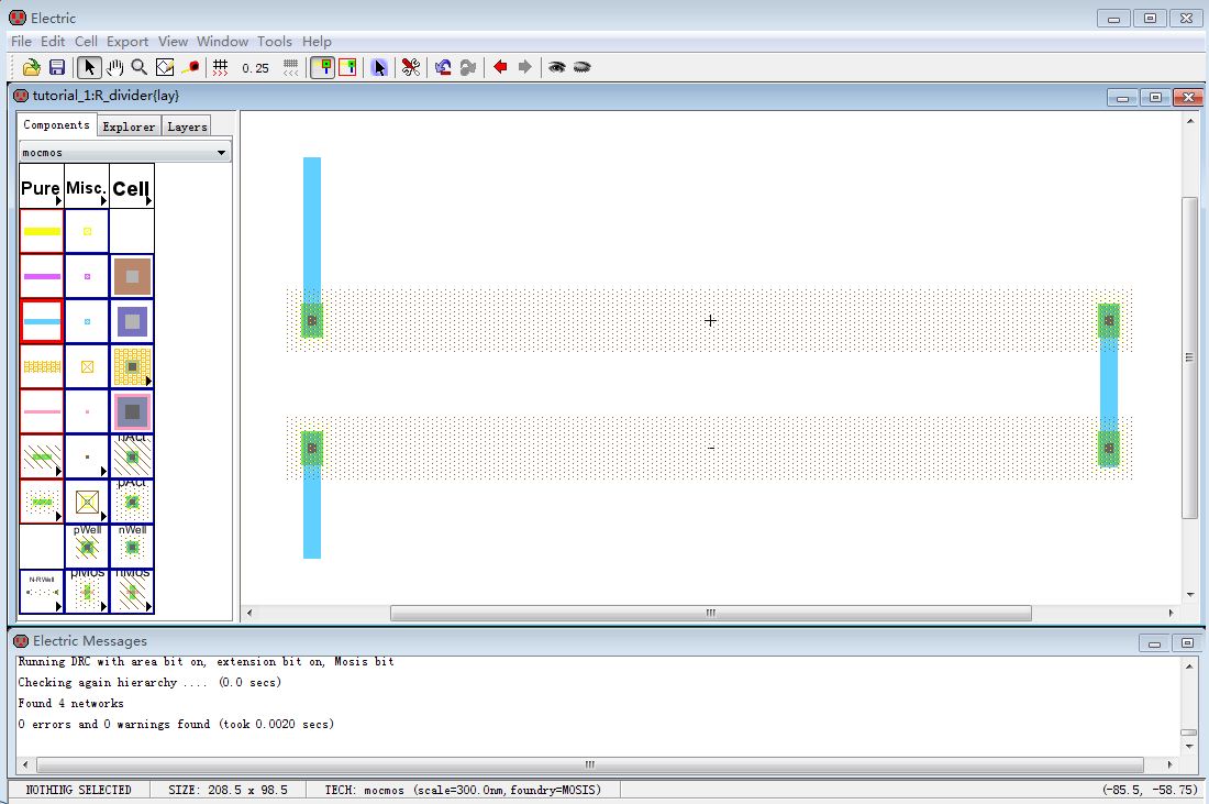
Press F5 or use Tools-->DRC-->Check Hierarchically to perform a design rule check. Notice there is no errors and no warnings in the Electric Message . If the layout has some errors, we need to check design rules to remove them(use ">" or "<" to check go forward or backward throught the errors and notice the discription of the error is indicated in the Message window ). Left figure is DRC without errors, the right one with some errors.


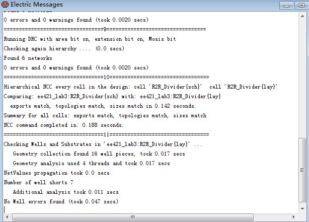
Next, use Network Consistency Checking (NCC) to check the layout versus schematic (LVS). We can use the Tools-->NCC-->Schematic and Layout Views of Cell or press the key binding "L". If there are a table pops up that allows you to click on the error to view it in a new window.
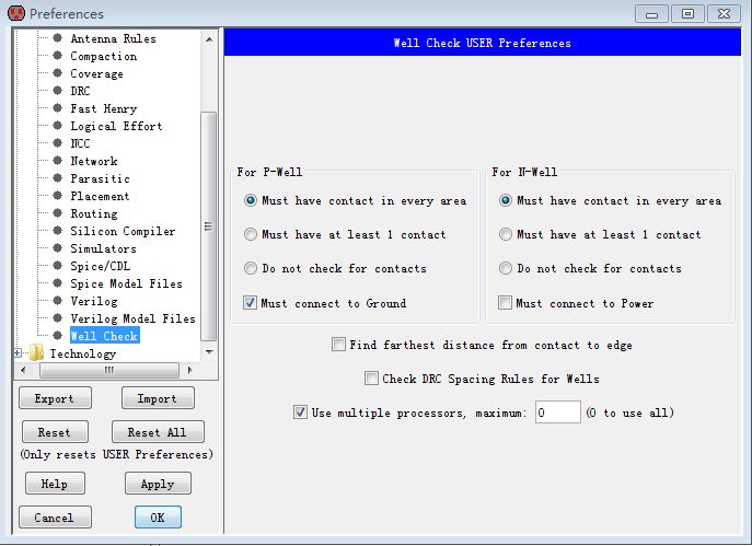
Then, one of the electrical rule checks(ERCs) is to verify that the p-well is always connected to ground in C5 process used in the tutorial. Setup the ERC well check go to Preferences --> Tools--> Well Check as seen below.

We have four aspect to verify that p-substrate is always tied to ground; a contact is found in every area for P-well; N-well must be connected to VDD and must have contact in every area. Press W or tools-->ERC-->Check Wells to run the well checker on the resisotr layout reporting some errors.
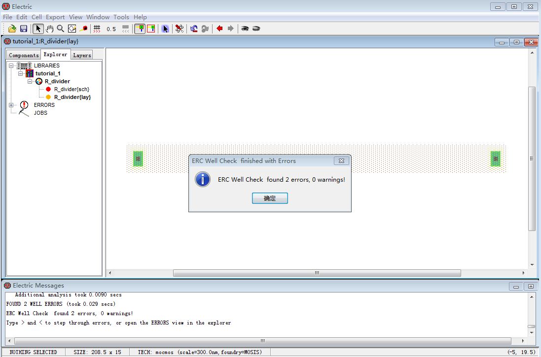
To remove these errors, we don't need to check N-well connect to VDD. So we go back change the settings. Running the Well checker again.
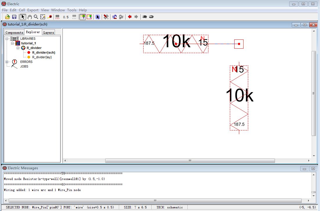
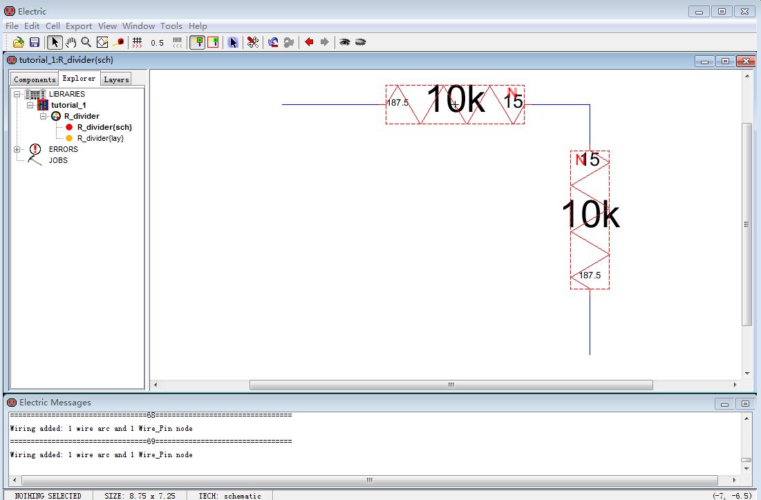
Now let's go to schematic model. Select N-well resistor node and use Ctrl+C and Ctrl+V to copy another one. We can get the following image.

Next, we use the Ctrl +R to rotate the bottom resistor and left click mouse to one side of resistor node and then right click to where you want to connect. The result is shown below.
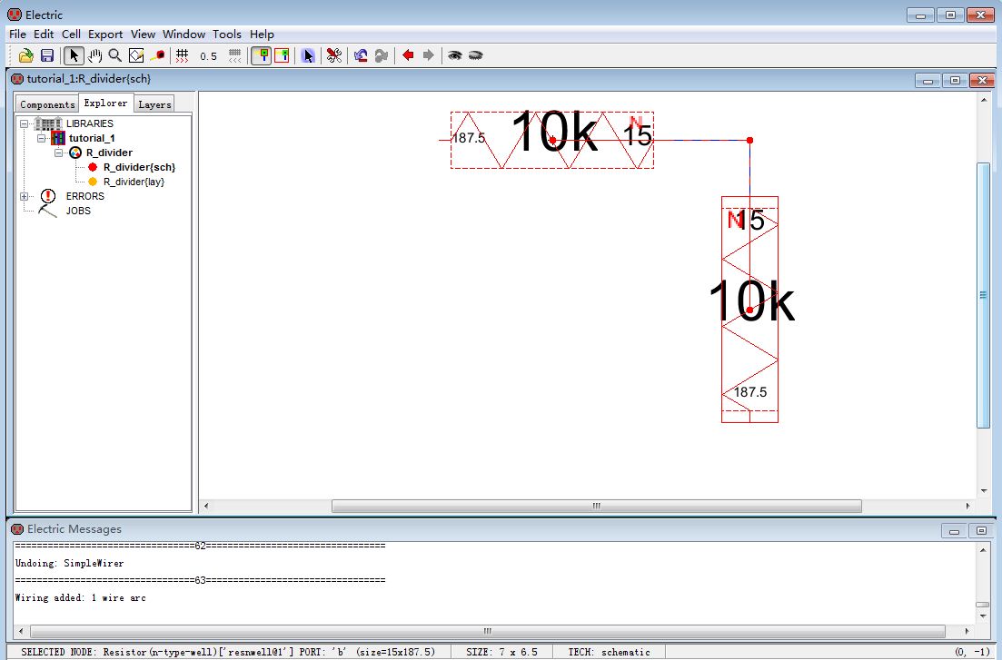
Maker sure no unnecessary pins in this schematic by removing by going to the menue item Edit-->Cleanup-->Cleanup Pins.
Next let's add more wires as seen below.

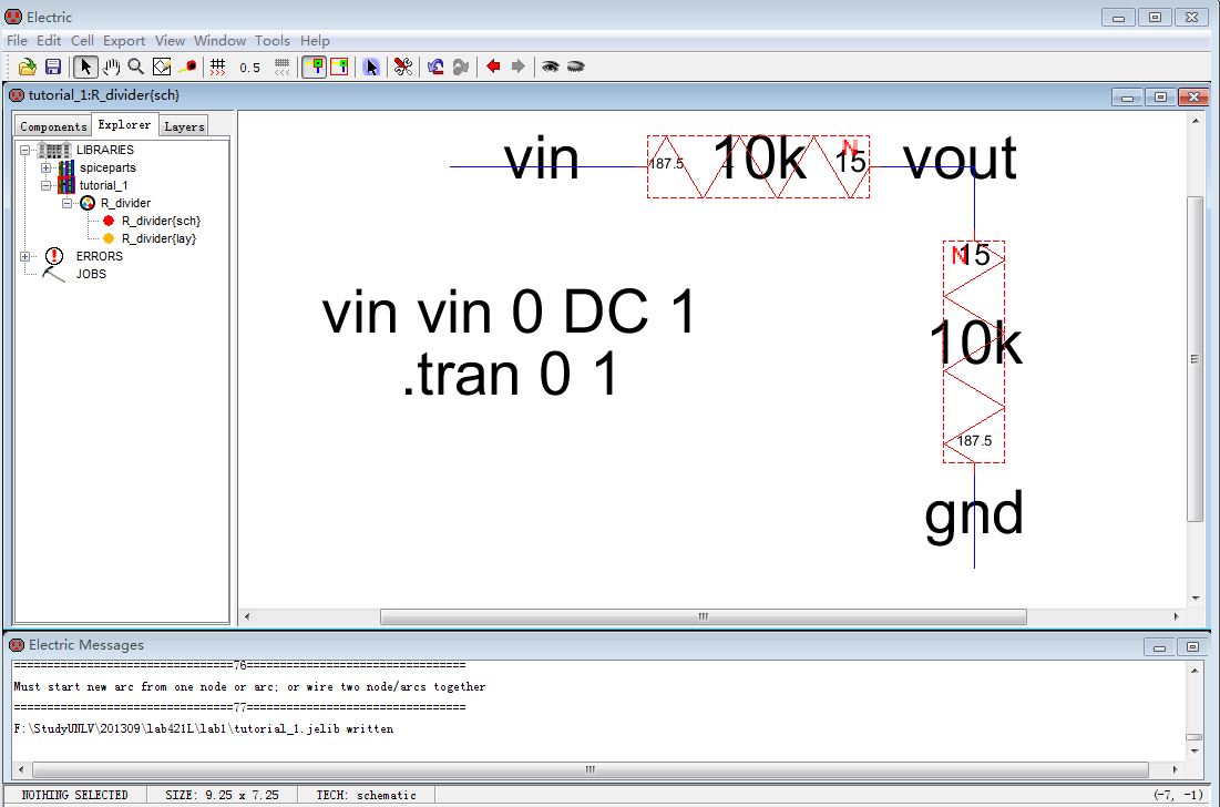
Then, we click the arrowhead in the MISC box in the component to add SPICE code. After that, press F5 to check the schematic and also save the library.
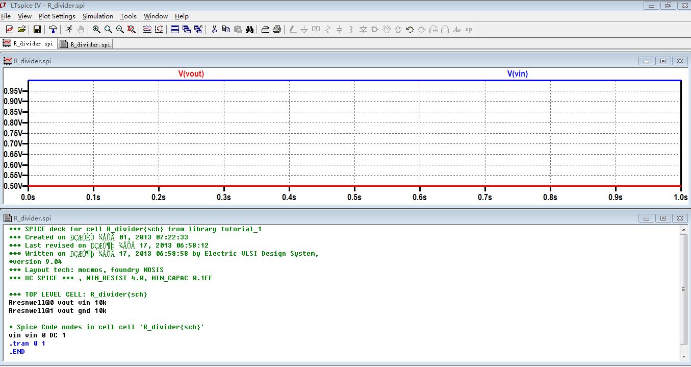
Now let's press S or Tools--> Simulation(Spice)-->Write Spice Deck to run the simulation. Click the plot icon in the LTspice window to get the simulation result as seen below.
In order to save dick space, we can setup the saving options. Click Tools-->Control Panel-->Operation and select No for .raw files and other files can be selected Yes to automatically delected.

When LTspice is closed, we can also use the Electric's probe. Only need to change from -i to -b modes when seeting LTspice up for use with Electric mentioned here.
Then we can use Electric's probe to watch the simulation result.

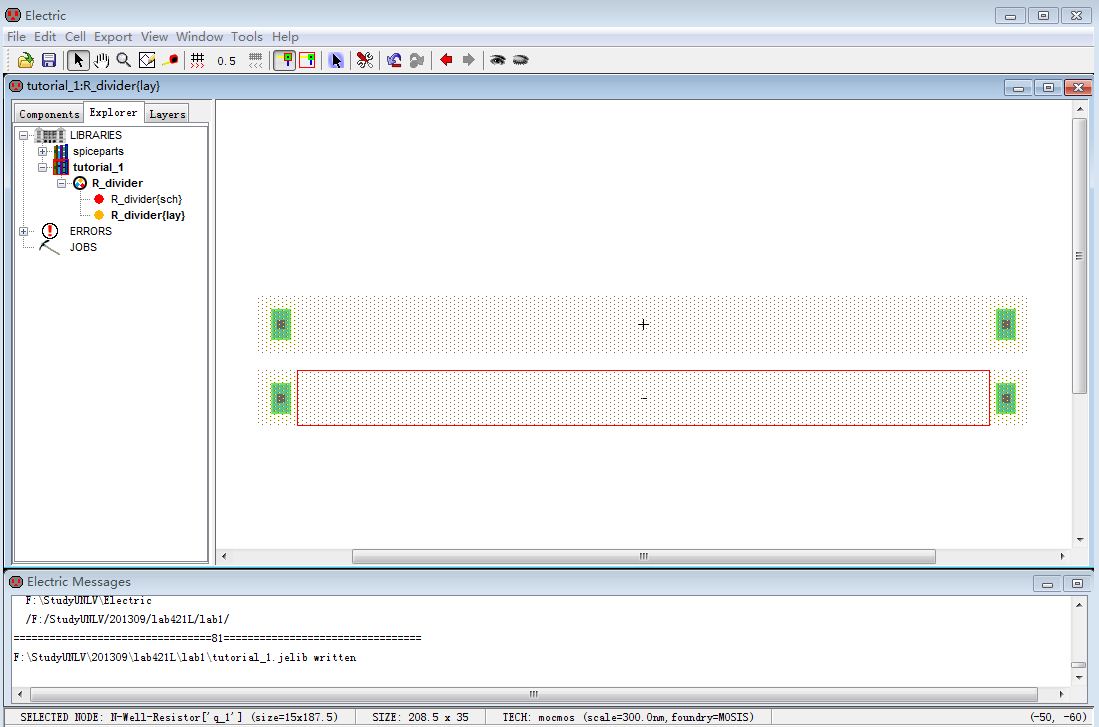
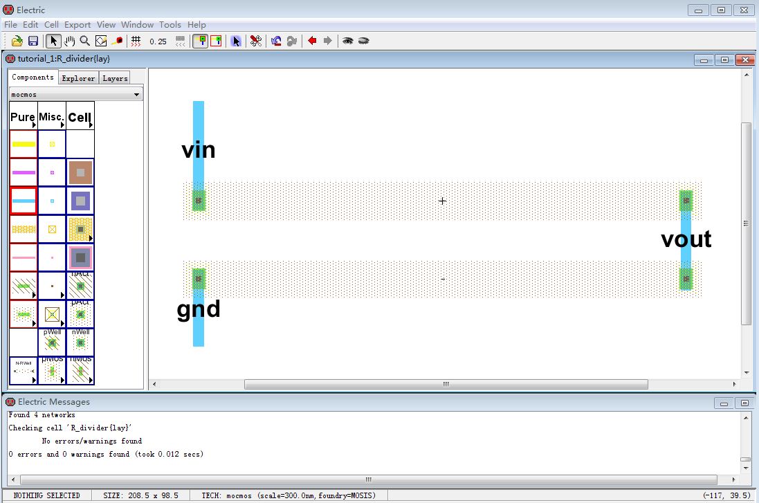
Now we step into the layout design of the resistor divider. Click layout cell and copy/paste to get two n-well resistor. Use mouse to drag or use the keyboard arrows to move the resistors.
Press F5 to check DRC and use "<"">" to check the error. Move the nodes unitll passing the DRCs.
Now left click the top resistor of its rightside and right click the down resistor rightside for using metal1 to connect them. And also use the left-right mouse click to design the layout like below. Using the DRC to check your layout.
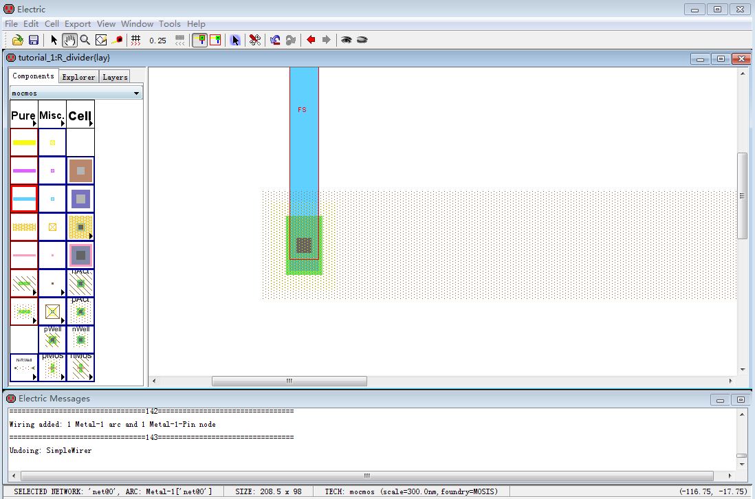
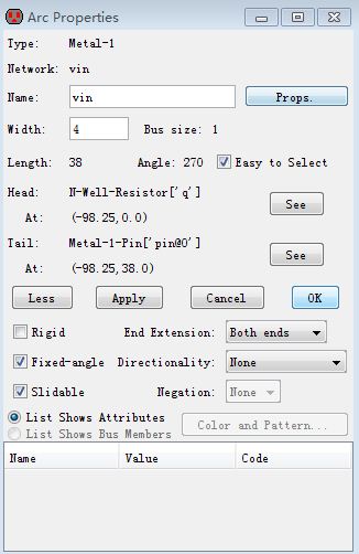
Then we need to increase the width of the metal 1 Arc to match the connection of the N-well resistor. Click the metal1 and Q or Ctrl+I to setup the width to 4 and hit OK.
Change all Arcs and run DRC to check the layout.
Next, change the name of each Arc and adjust the text size. After that, you can get the layout like below.

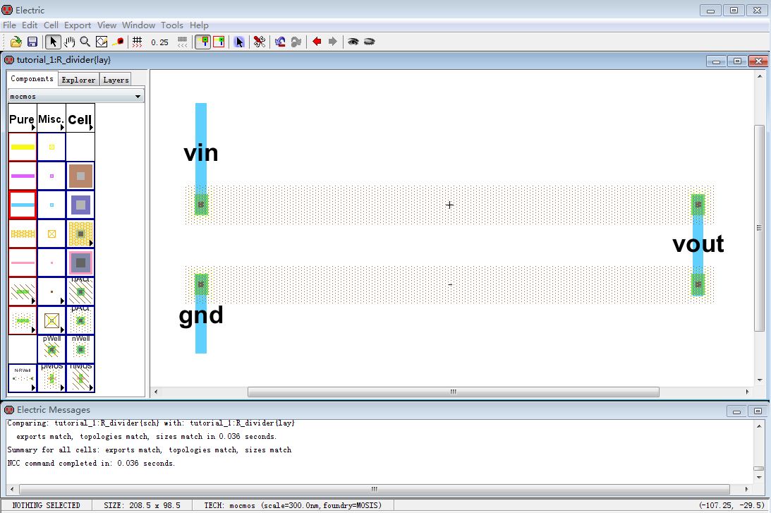
Now we can verify the layout by running the NCC.
And copy the spice code in the schematic model and paste in the layout cell.
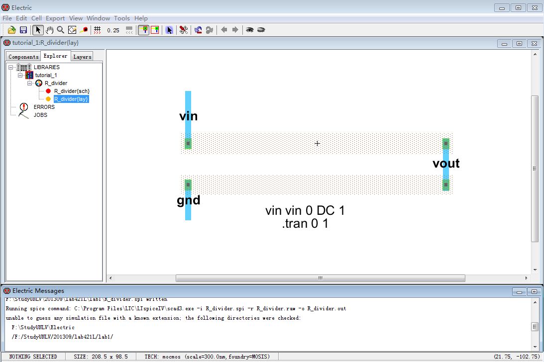
Last but not least, run DRC, NCC, ERC to check this layout and make sure there are no errors. Then press "S" to run the simulation and get the result.

Backup the design directory (tutorial_1.jelib) and move the layout design of a R2R DAC.
A 10-b R2R DAC Layout Design
1. How to select the width and length of the N-well resistor.
Submicron design rule of C5 process requires the minimum width of N-Well, 12lambda. I set the width of the N-well resistor is 15lambda. And The MOSIS Data sheet shows the sheet resistance of N-well is 800ohms/sq. For a 10k resistor, the length should be 187.5lambda (10k/800*15). The resistor property is shown as below.

2. How to measure the width and length by Electric
Electric provides the Toggle Measure Distance to help us the meaure. Actually in the real resistor layout, the length is more than 187.5lambda (dx highlighted by the blue pen as seen below). We setup the length above meaning the distance between two contacts(dx highlighted by the red pen as seen below). The width is highlighted by the black pen.

3. Design the DAC Layout
Considering the minimum spacing between wells at different potential is 18lambda, I redesign the R2R divider as seen below and create a P+ ring to reduce the noise. Use Ctrol+E to name the exports and ground the P+ ring.

The following image is the R2R divider schematic and icon by using three 10k n-well resistors.
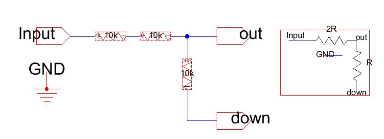
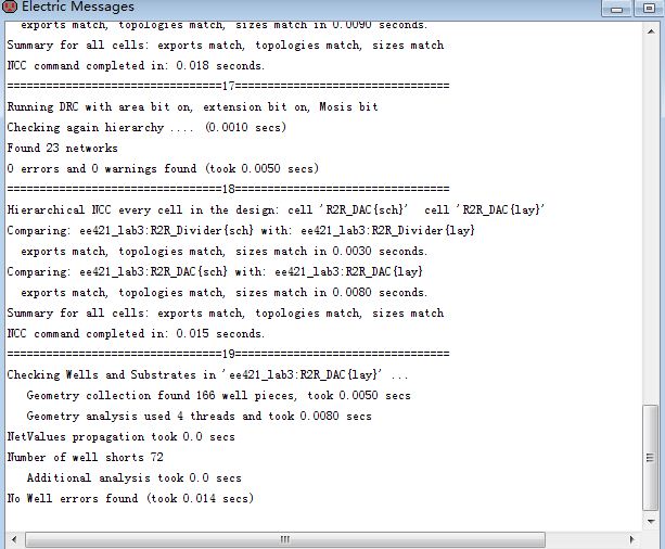
As the basic circuit in the DAC, I verify the DRC, ERC, NCC of the R2R resistor without errors.
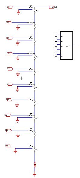
Next design the schematic of the DAC. Drag one icon to the new cell and use the array command (F6) to put 10 icons of the R2R resistor divider in parallel. Then set the export names and make a icon as seen below.
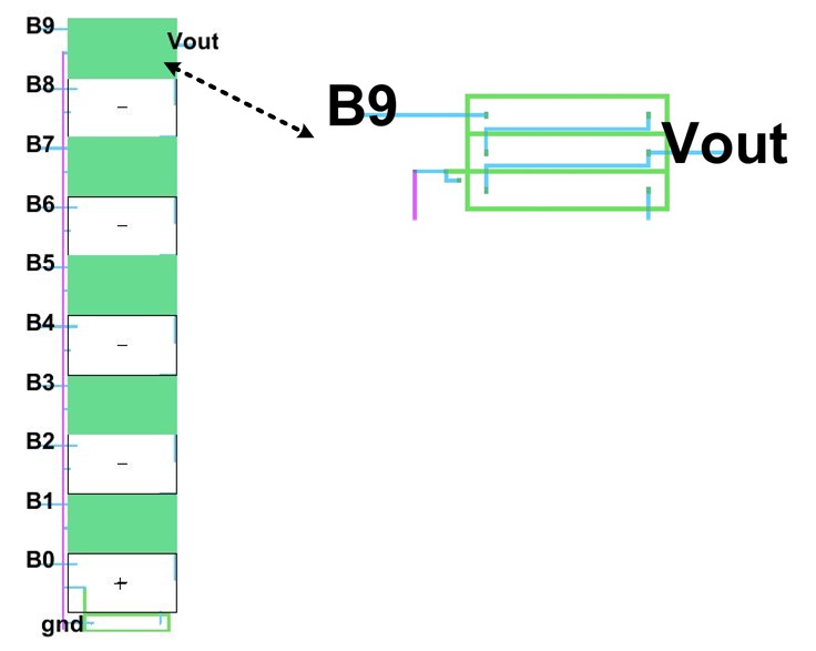
Now let's design the layout. Drag the layout cell into the R2R_DAC{lay} and make a array having 10 icons. Add one 10k N-well resistor on the bottom. Use metal1 to connect 10 numbers of output nodes, 1 output and 1 gnd. Notice that I use via1 and metal2 to connect all the gnd together.
Run DRC,ERC, NCC again to check no errors in this layout as shown below.
Finally, backup your design ee421_lab3.jelib directory and other files for future study.