Lab 1 - ECE 421L
Authored
by: WENLAN WU (Stephen)
E-mail: wuw2@unlv.nevada.edu
Date: 8/30/2013
Lab
description
Lab 1 goes through the tutorial_1 of Electric from CMOSedu.com. The report consists of two steps.
1. Follow
the tutorial_1, capture the fist 10 pictures to understand some
basic settings of Electric and add components.
2. Backup the Lab report and upload it to the CMOSedu.com for the future study and discussion.
Discussions & Captured Images following Tutorial_1:
1.) Firstly, I open the Electric software and the work window is grey color.
2.) Secondly, I change the work-window into white color by choosing Window--> Color schemes--> White background colors.
3.)
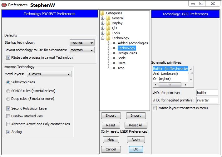
Thirdly, for use in ON Semiconductor's C5 process, I set up the
Electric technology in the design library. It has three layers and
fabricated through MOSIS. (PS: This tutorial uses the MOSIS scalable
CMOS submicron design rules)
Go
to File --> Preferences--> Technology--> Technology and make
sure the information to match what is seen in tutorial_1.
4.)
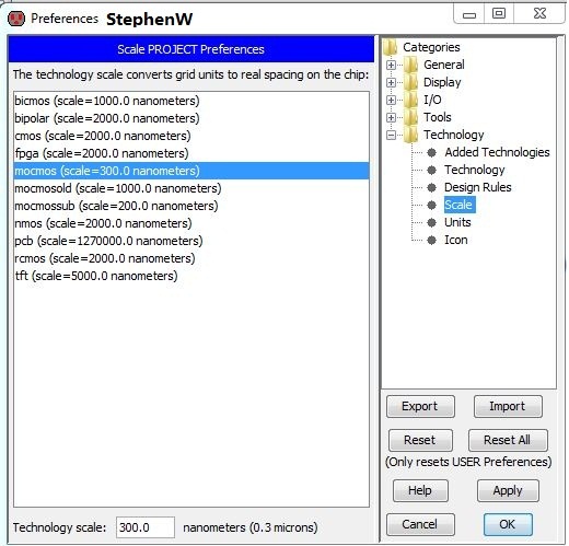
Then, I use the MOSIS Scalable CMOS and set 300nm as the
scale (lambda) for the C5 process by going to File -->
Preference --> Technology --> Scale. After that, press OK.
5.) After setting up these above, I import the electriPrefs.xml(from Dr. Baker) because circuit design using keyboard is very convenient and professional.
Then, I click File --> Save Libraray As --> tutorial_1.jelib.
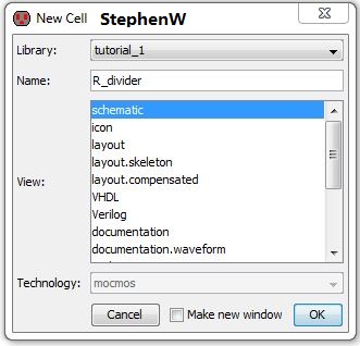
Next,
I begin to draw a schematic of a resistor in tutorial_1.jelib. In the
beginning, I have to open a new cell, go to Cell --> New Cell and
enter the information like the following image(name: R_divider and
view: schematic). Then, press OK.
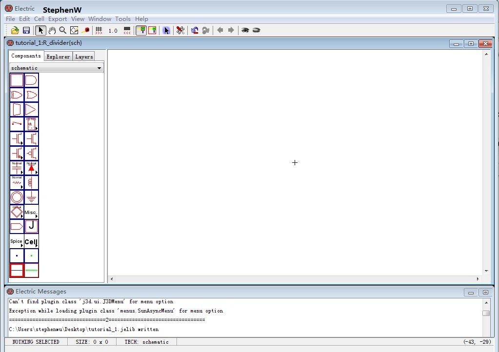
6.)
I select the component tab on the left side and see lots of basic
circuit components. Besides the component tab, Explorer and Layers tab
are also very important. The first one is to show the cells in the
design library. The later one is to turn on/off the display of certain
layers in the layout design.
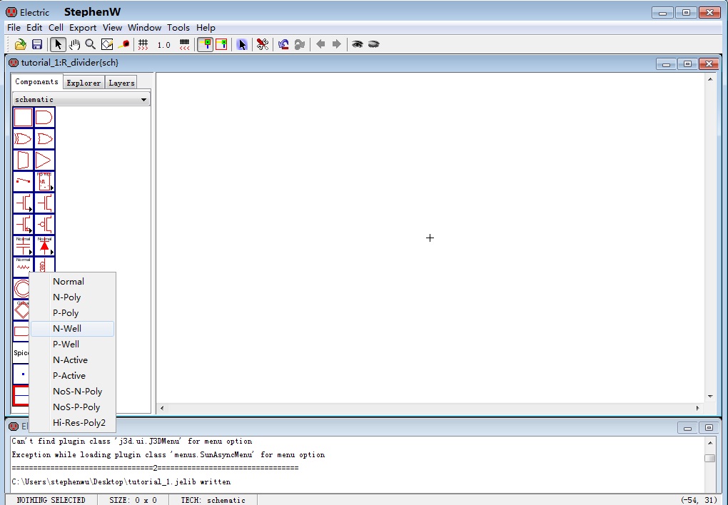
7.)
I select the box containing a resistor and the word "normal". And click
on the arrowhead to select N-Well. Then click the white work-window so
that the N-Well resistor could be shown up.
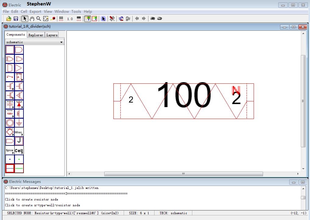
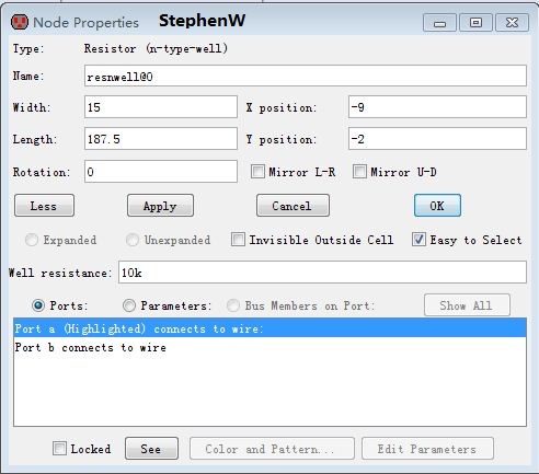
8.)
I press "q" to open the object propoerties (Go to Edit -->
Properties --> Object Properties is the same.). And then I set the
resistance "10k", width=15, and length=187.5. After that, I also select
the "Port a (Highlighted) connects to wire".
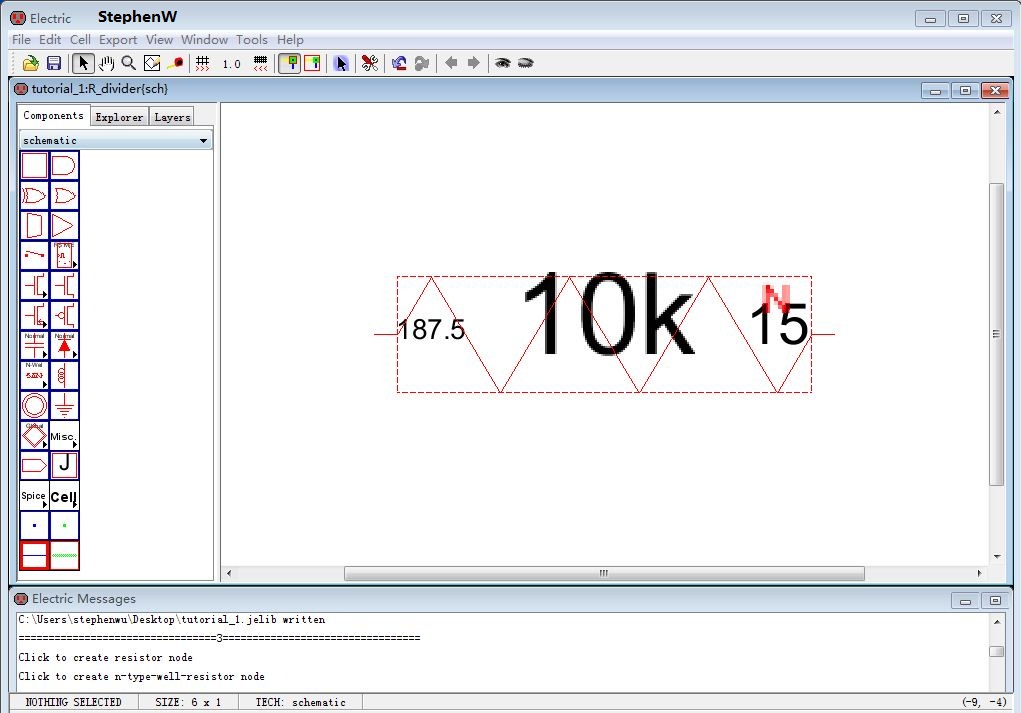
9.) Press "OK" and I see the following image. This is a 10k N-Well resistor schematic.
Backup:
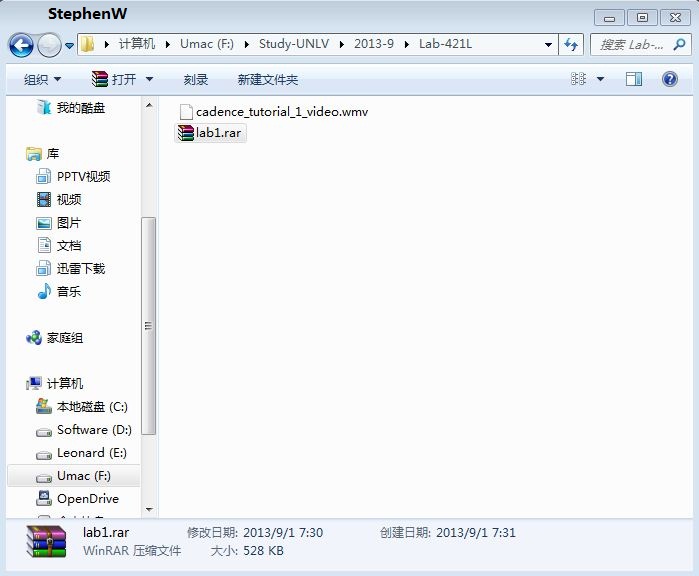
Right
click the mouse to compress the lab1 fold into "lab1.rar". And then put
the backup file into my study folder and also email to myself.
Return to the listing of my labs
Return to the whole class reports
Return to the EE421L
Return to the CMOSedu.com