Lab 3 - EE 421L Fall 2021
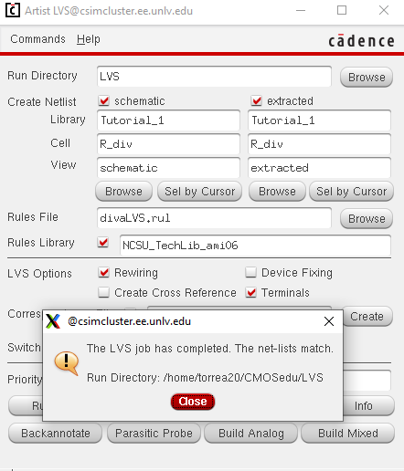
The next part of the pre-lab is to finish Tutorial 1 which is the layout of the voltage divider circuit followed by DRC and LVS checks. The following figures are the layout and extracted view of the voltage divider.
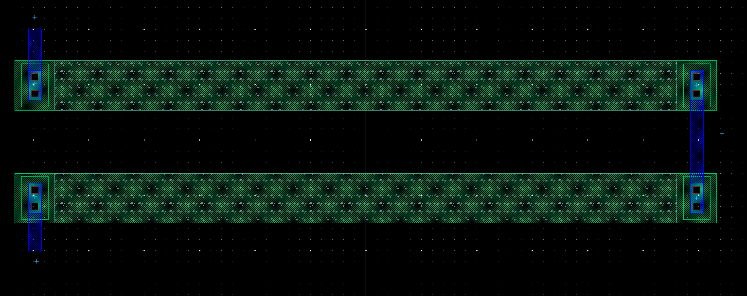
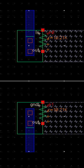
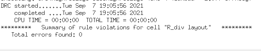
The next step is to DRC the layout to ensure that there are no errors within the design shown below. Once the layout has been DRC and you have the extracted view you must LVS the schematic and extracted views to ensure the physical implementation of the netlist.
In this lab we will do the layout of the 10-bit DAC and run DRC and LVS checks to ensure the netlist match. Below you may find what is included in that lab.
- We start with the voltage divider that acts as 1-bit which was created in the previous lab found here
- That layout is then used to build the 10-bit DAC
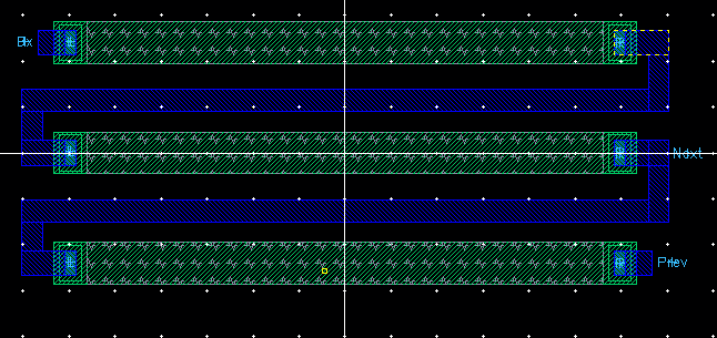
This design is the layout of the voltage divider used as 1-bit it was built of the 10k ohm resister created in Tutorial 1. In order to correctly aquire the 10k ohm resister the following values where used:
- Width (4.5um) , Length(56um), Sheet Resitance(800 ohms)
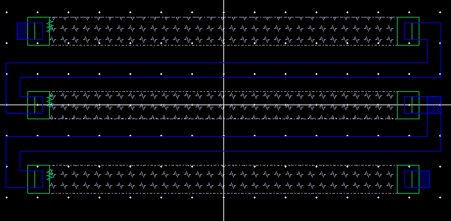
The reason that these values work is because the Resistance value is based on the equation (R = Rsquare*(L/W)) . Shown below is the layout and extracted view of the 1-bit voltage divider followed by the LVS check to ensure the netlist match.
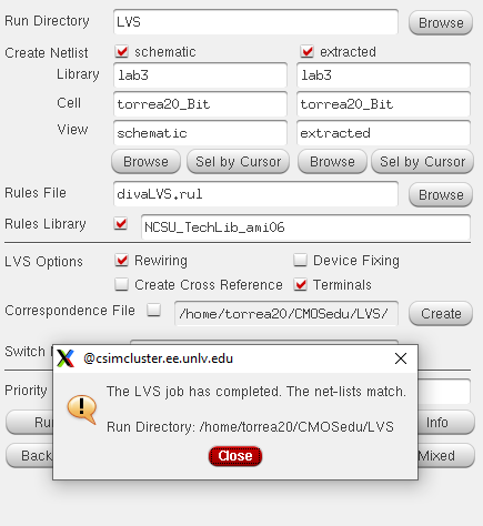
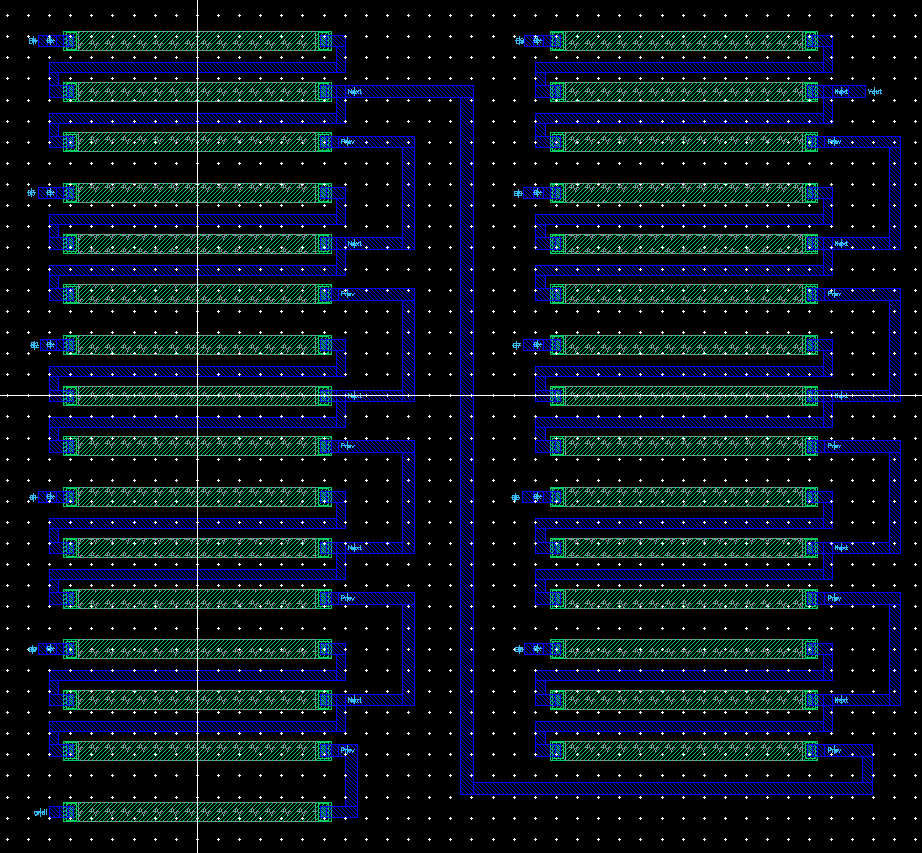
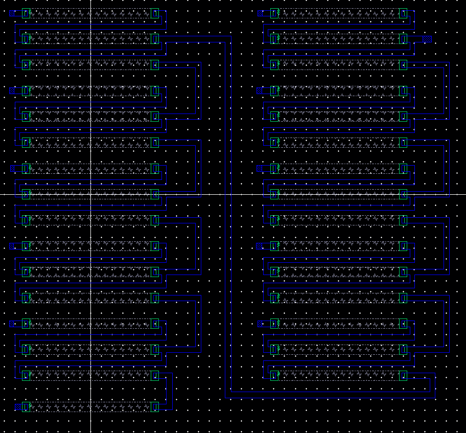
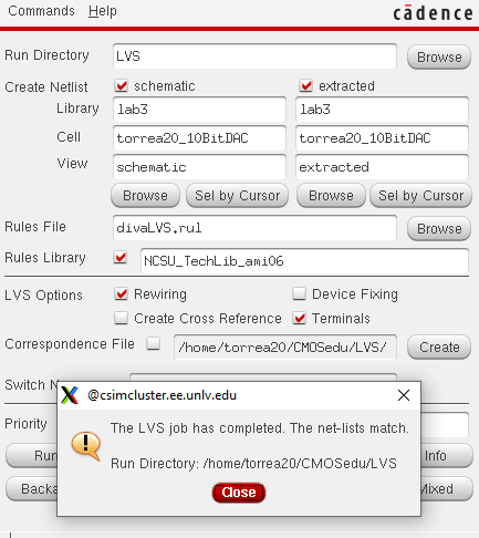
The 1-bit voltage divider is the basis of the 10-bit DAC this is because I know that there will only be issues on the top layor. In this layout shown below each bit was wired together to act as the 10-bit DAC shown by the schematic shown in the previous lab. Once the layout was created with no DRC errors the extracted view was created which is shown below. The last step was to LVS the design to ensure that the netlist matched.
A link to the final design of the 10-bit DAC can be downloaded here