Lab 2 - EE 421L Fall 2021
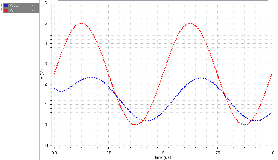
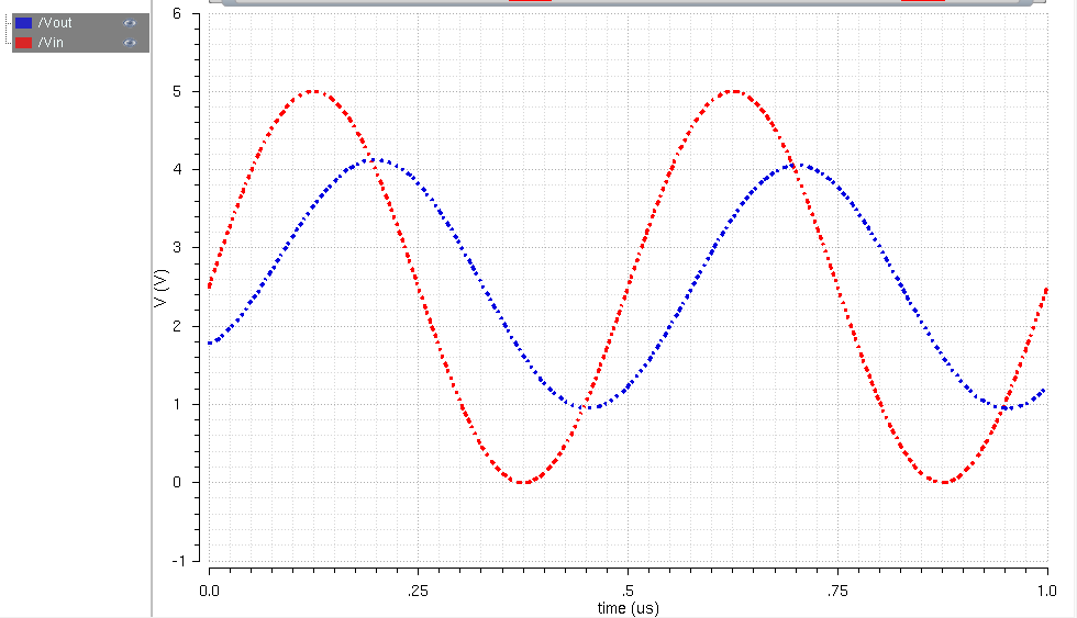
After the schematic was opened I ran the simulation as it was to see and by messing with the Vin and I noticed that the steps on Vout will lower as Vin decreases.
In order to show my understanding of the circuit I changed Vin to 5mV to show a better comparison to the orginal and as mentioned before the amount of steps on Vout decreases and the input voltage decreases. This is because the steps is based upon the Least Signficant bit and follows the equation (VDD/2^n) where VDD is given as 5V and n is 10 for the 10 bits. This equation is given in Figure 30.14 in the lab manual found here.
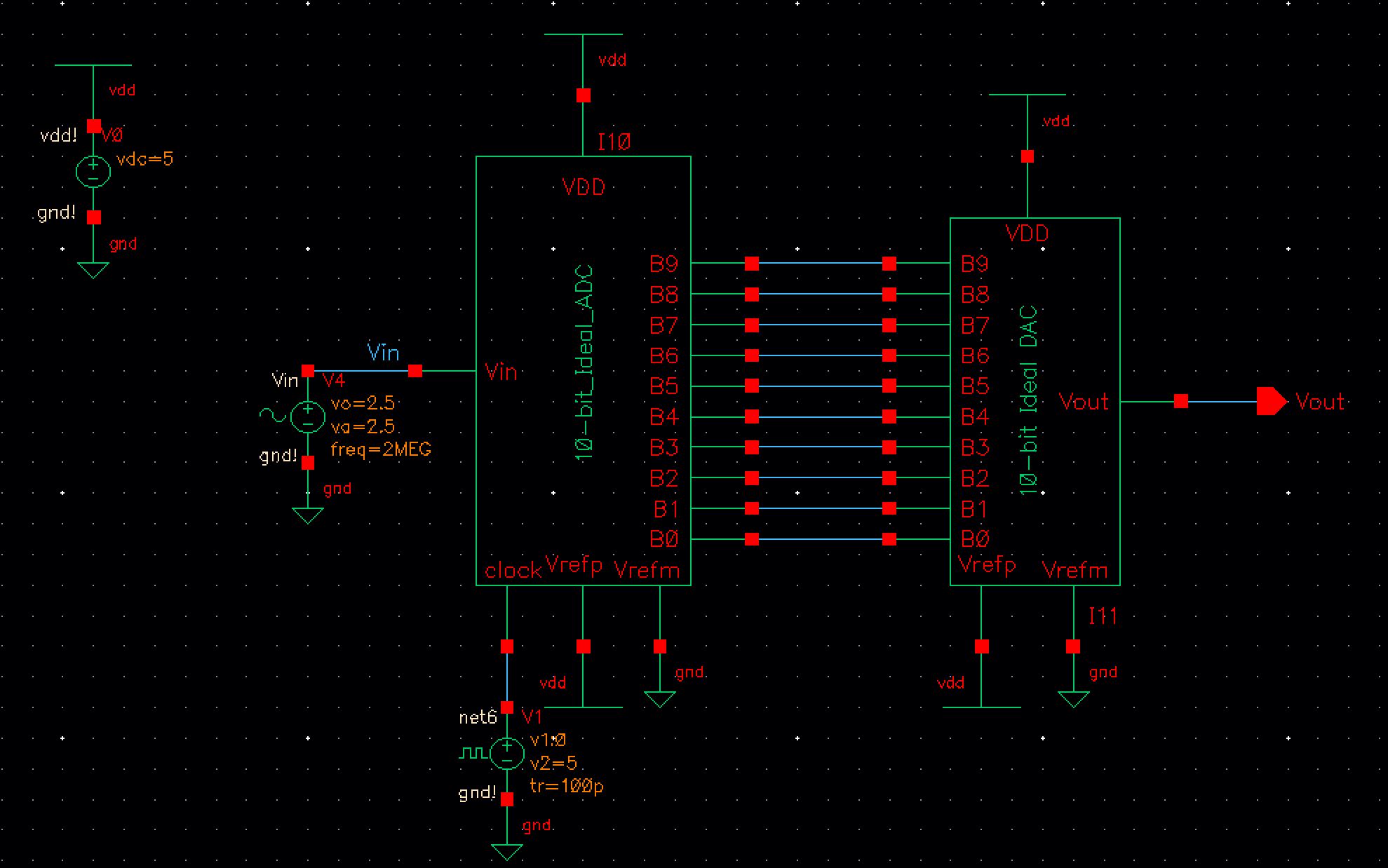
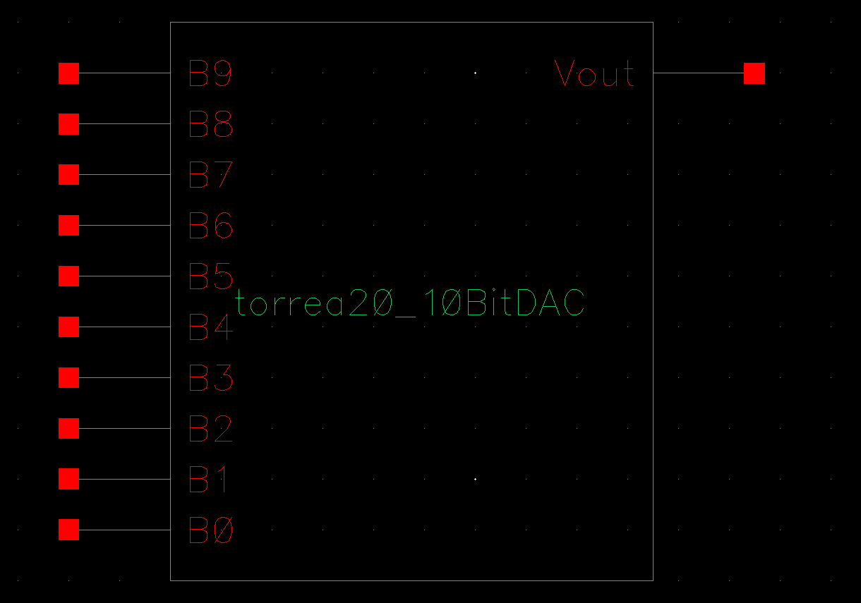
In this lab we implement a 10-bit DAC to the controlling input bits from the ADC provided in the lab2.zip file. The DAC we create is based upon Fig. 30.14 in the CMOSedu book and compared to the ideal DAC provided in the zip file. A breakdown of what is included in the lab is as follows:
- Creation of 10-bit DAC
- Hand Calculations of output resistance
- Simulation of delay of DAC driving 10pF load
- Multiple simulations replacing ideal DAC with DAC created in the lab
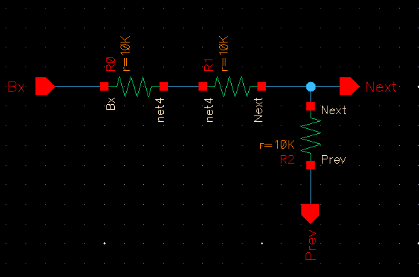
The first step in creating the DAC is the basic schematic for one bit as seen below followed by the symbol created.

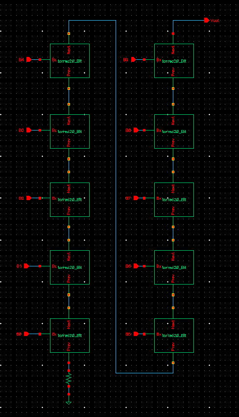
The next step is creating a new schematic which is a 10-bit DAC comprised of the 1 bit symbol created before. After the schematic is connected corretly a new symbol is created titled (torrea20_10BitDAC) which will be used to run the simulations.
The next part of the lab is doing the hand calculations to solve for the output resistance of DAC.
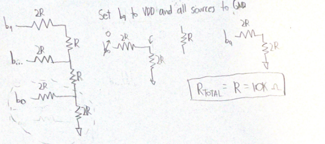
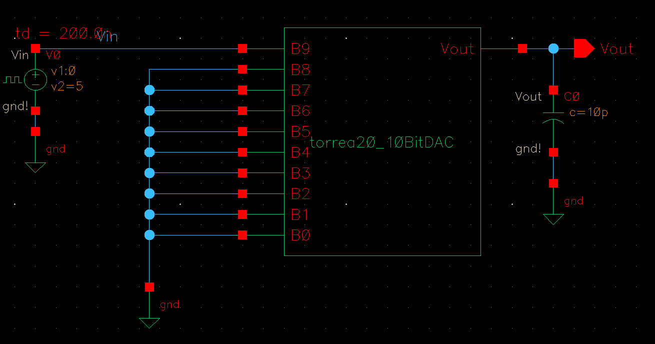
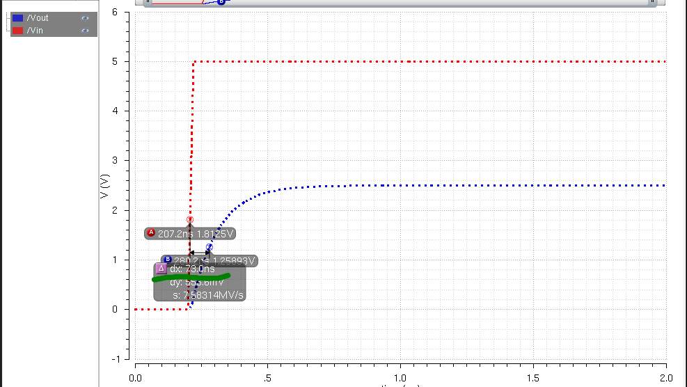
Using the output resistance the delay through DAC driving a 10pF load is found by td = .7RC (td = .7*10k*10p) therefor td = 70nS. In order to verify this through simulation the created DAC circuit is tested by having B9 pulsing from GND to VDD and having all other inputs set to GND. Once this is done we can see that the dealy is given by the difference between the 50% mark of the output to the rising pulse of the input in this case being 73nS.
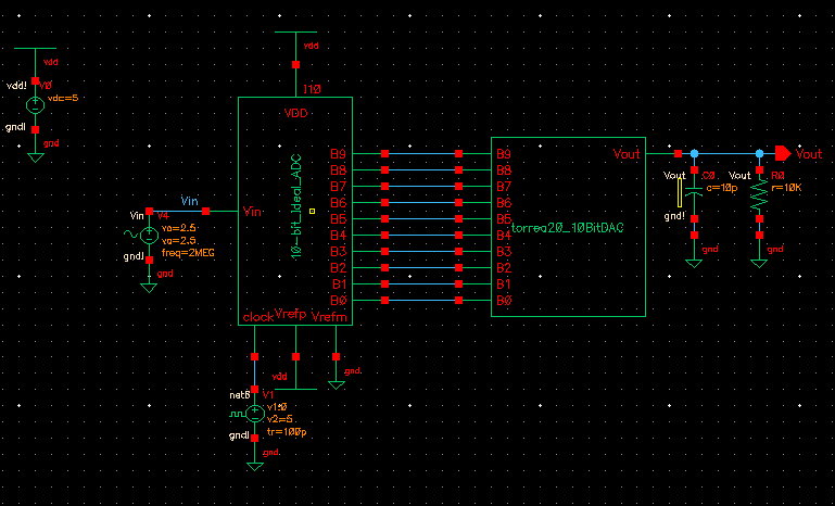
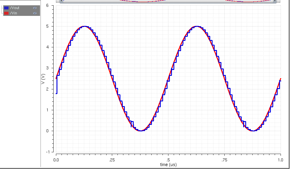
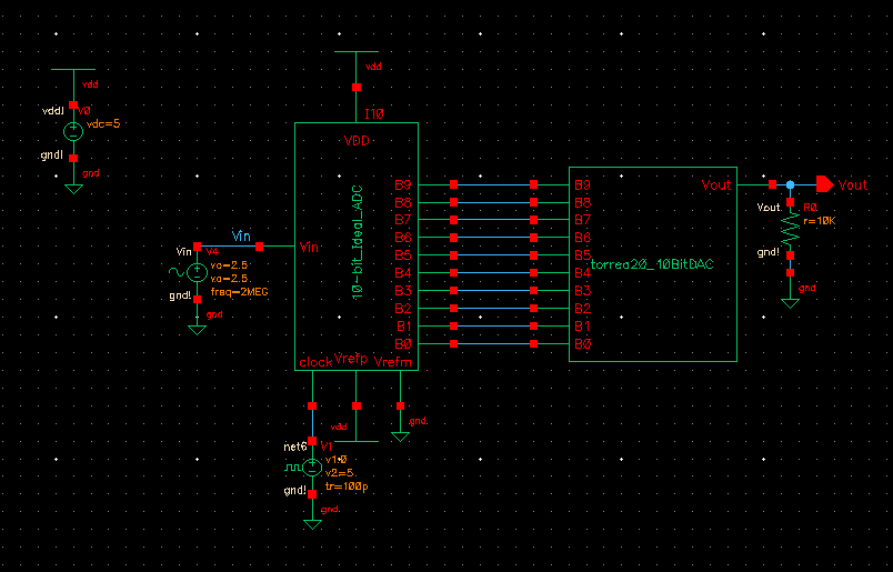
The final part of the lab is replacing the ideal DAC with the created DAC and running simulations given the differents.
- No Load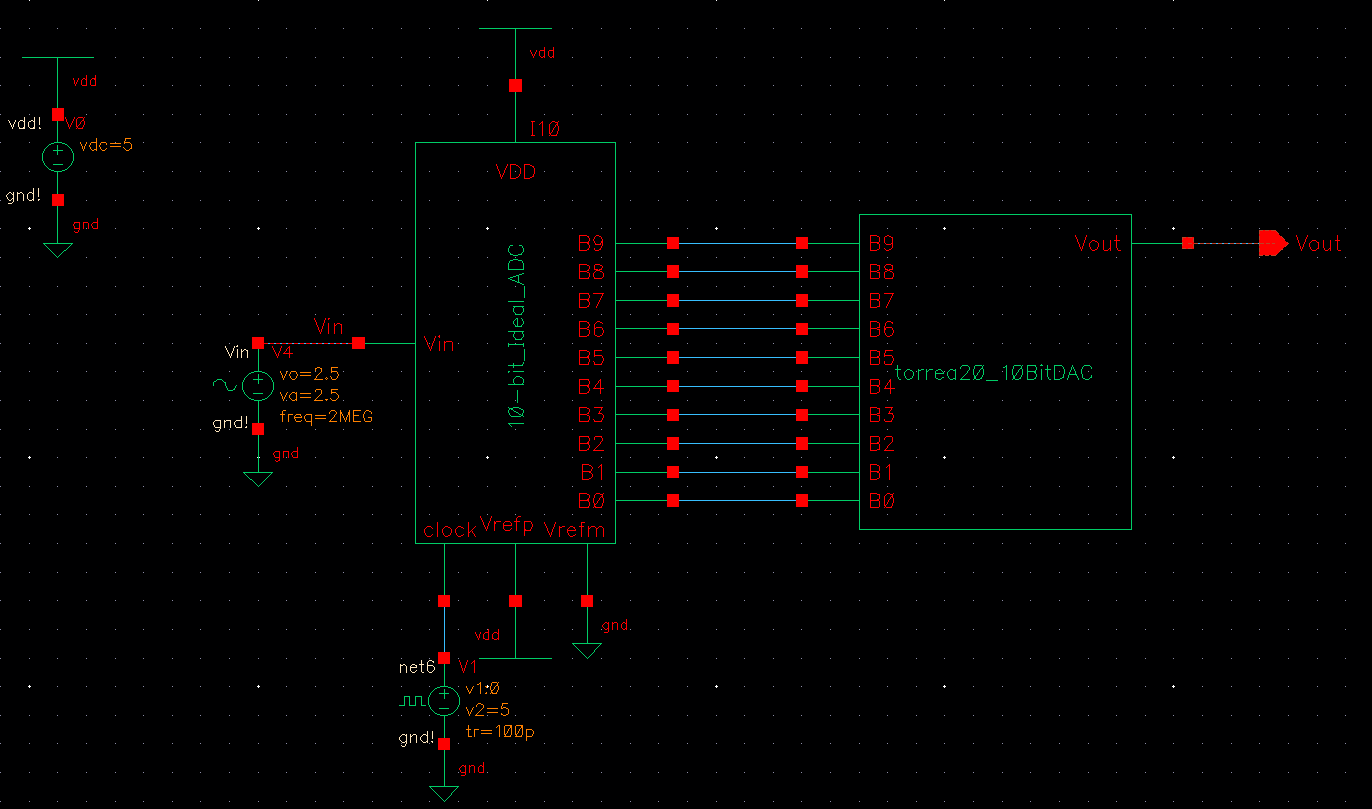
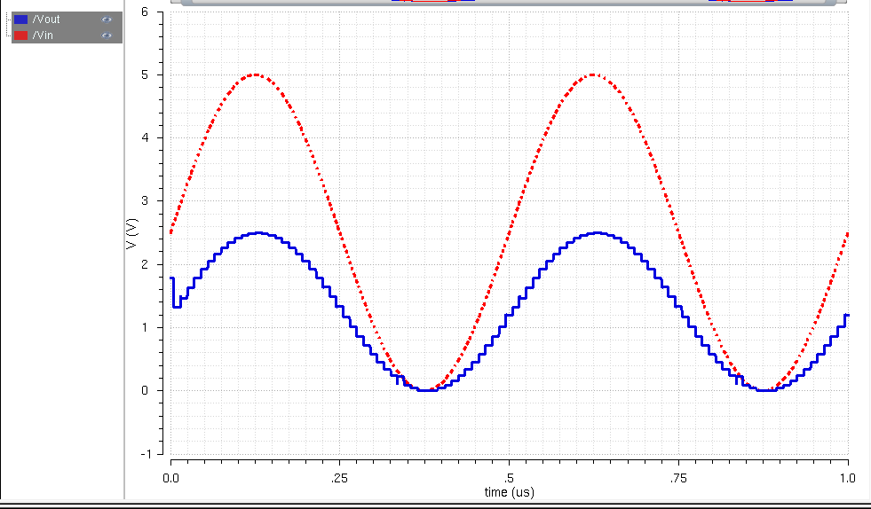
- 10k ohm Load
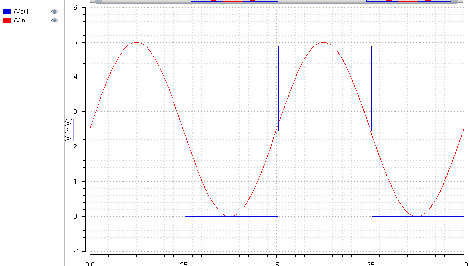
- In this condition the digial signal produced will be cut in half because the output resistance 10k ohms is now in series with the 10k ohm load creating a voltage divider which cuts the signal produced in half.
- 10pF load
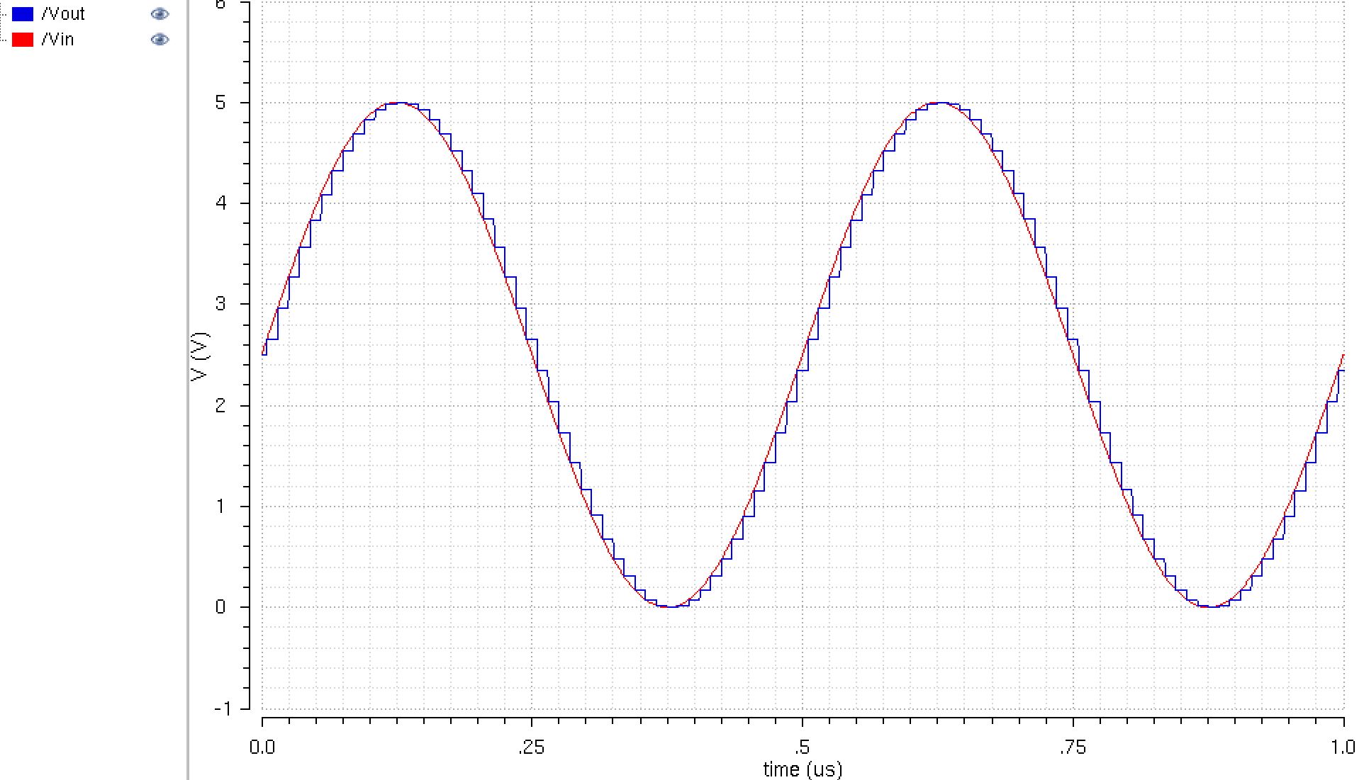
- In this condition the digial signal produced resembles that of a analog signal however due to the load the signal recives a 70nS delay a different voltage because of charging and discharging of the load.
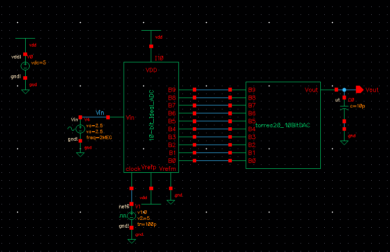
- 10pF and 10k ohm loads
- In this condition the digial signal produced is a combination of the previous the output is cut in half because of the voltage divider created the signal is delayed and the voltage is swing differs because of the 10pF capacitor.