EE 421L
Digital
Integrated Circuit Design Laboratory
Laboratory 4: IV Characteristics and
Layout of NMOS and PMOS devices in ON’s C5 Process
AUTHOR:
Bryan Kerstetter
EMAIL:
kerstett@unlv.nevada.edu
SEPTEMBER 25, 2019
General
Overview
This laboratory
introduces the MOSFET (the Metal Oxide Semiconductor Field Effect Transistor). This laboratory touches upon laying out both the
NMOS and the PMOS in the C5 process. These laid out MOSFETs are then
characterized. This laboratory is similar to another laboratory that I took (EE
420L: Characterization of the CD4007 CMOS Transistor Array).
Prelab
All previous laboratory work has been backed up.
Three terminal NMOS used to create symbol.

Figure 1
Symbol created from schematic.

Figure 2
Circuit designed to characterize NMOS.

Figure 3
Here, we can see the triode and saturation regions
of the MOSFET with varying gate to source voltages.

Figure 4
Here we see the layout of PMOS.

Figure 5
The extracted view indicates that there are indeed
four pins of the NMOS. The three terminal MOSFET has a hidden fourth pin. This
hidden fourth pin is assumed to be automatically connected to ground in the
schematic. In layout, the bulk of the transistor is not connected to ground.
Therefore, the layout will not LVS.

Figure 6
The layout is modified to accommodate a MOSFET bulk
connection.

Figure 7
The final layout of the NMOS passes the DRC.

Extracted view of the NMOS layout.

Figure 8
Does not pass the LVS because we are using a three
terminal MOSFET in the schematic.

Figure 9
Does not LVS
because the 4 terminal NMOS is needed in the schematic. Therefore, the four
terminal NMOS is used with the bulk connected to ground.

Figure 10
LVS is run again and this time the netlists of the
schematic and the layout match.

Figure 11
The extracted layout was then simulated. It is noted
that the extracted simulation matches the schematic simulation.

Figure 12
Simulation -> Netlist -> Display to
ensure extracted simulation.

Figure 13
PMOS
Now all the previous steps are performed for the
complimentary MOS, the PMOS.

Figure 14
A symbol was created for the PMOS.

Figure 15
A layout was made for the PMOS.

Figure 16
Passes DRC:

Figure 17
Extracted View:

Figure 18
Circuit designed to characterize the PMOS.
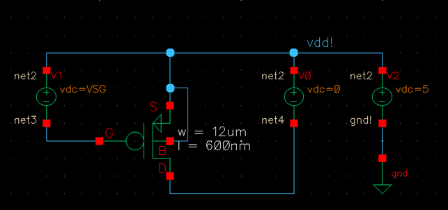
Figure 19
Schematic Simulation

Figure 20
Extracted Simulation

Figure 21

Figure 22
Laboratory Procedure
MOSFET Characterization in the C5 Process
1. A schematic for simulating ID v. VDS of an NMOS device for VGS varying from
0 to 5 V in 1 V steps while VDS varies from 0 to 5 V in 1 mV steps. Use a
6u/600n width-to-length ratio.
Schematic:

Figure 23
Simulation:

Figure 24
2. A schematic for simulating ID v. VGS of an NMOS device for VDS = 100 mV where
VGS varies from 0 to 2 V in 1 mV steps. Again, use a 6u/600n width-to-length
ratio.
Schematic:

Figure 25
Simulation:

Figure 26
Note, this indicates that the threshold voltage for the NMOS is around
0.7 volts.
3. A schematic for simulating ID v. VSD (note VSD
not VDS) of a PMOS device for VSG (not VGS) varying from 0 to 5 V in 1 V steps
while VSD varies from 0 to 5 V in 1 mV steps. Use a 12u/600n width-to-length
ratio.
Schematic:

Figure 27
Simulation:

Figure 28
4. A schematic for simulating ID v. VSG of a PMOS device for VSD = 100 mV where
VSG varies from 0 to 2 V in 1 mV steps. Again, use a 12u/600n width-to-length
ratio.
Schematic:

Figure 29
Simulation:

Figure 30
Here we can see that the threshold for PMOS is around 0.9 volts.
The Probing Pad
The following is the specifics of the rules regarding probing pads (as
provided by MOSIS).
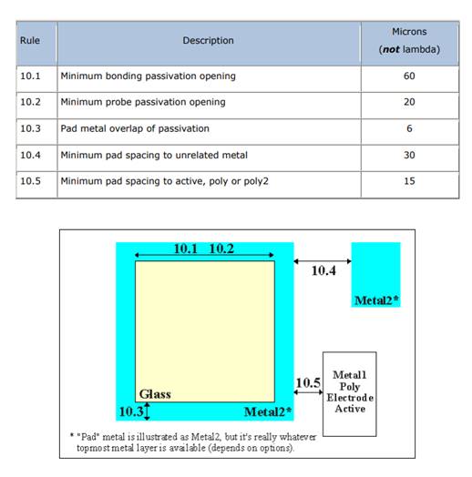
Figure 31
Here are the dimensions of the probing pad that was designed.

Figure 32
Here we created a schematic for the probing pad.

Figure 33
From the schematic we created a symbol so that
eventually our design can go through a LVS.

Figure 34
Lay Out NMOS with Pads
The NMOS symbol (Figure 35) and layout (Figure 36) was modified and
passed DRC (Figure 37) and LVS (Figure 38).

Figure 35

Figure 36

Figure 37

Figure 38
A schematic was created.

Figure 39
The schematic was then translated into a layout.

Figure 40
Here is a closer view of the layout.

Figure 41
Here is the extracted view of the layout.

Figure 42
The layout passes both DRC and LVS.

Figure 43
The symbol was modified so that one may easily identify
the NMOS has probing points attached to all four terminals.

Figure 44
We then used the following schematic to ensure that
our layout functions properly.

Figure 45
The simulation testifies to the fact that our layout
functions properly.

Figure 46
It was ensured that the simulation simulated was the
extracted cell.

Figure 47
Lay Out PMOS with Pads
The following circuit was created.

Figure 48
Here is the final layout of the PMOS connected to four pads.

Figure 49
Here is a closer view of the layout.
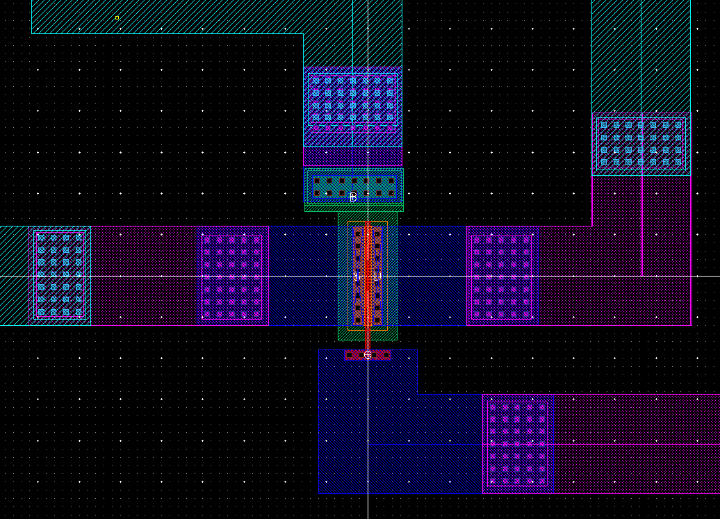
Figure 50
Here is the extracted view of the layout.

Figure 51
Our layout passes both the DRC and the LVS.

Figure 52
The following symbol was created to indicate a PMOS
with probing points attached to all 4 terminals.

Figure 53
The following circuit was used to determine if the
laid out PMOS properly functions.
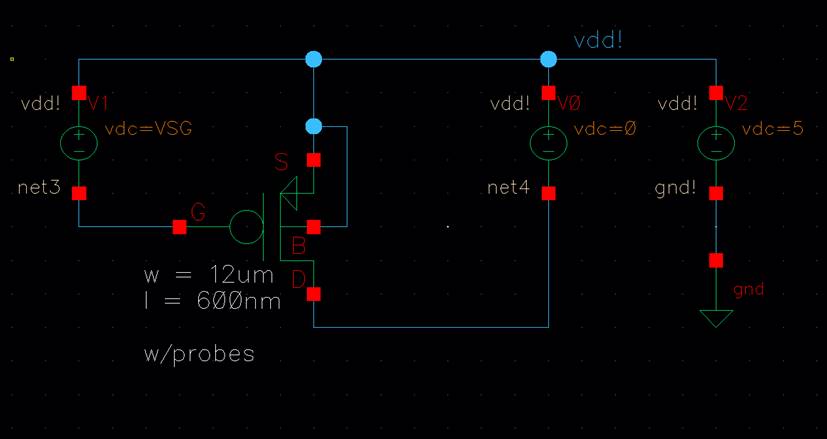
Figure 54
The simulation as seen in Figure 55 testifies that our
laid out PMOS properly functions.

Figure 55
It was ensured that the extracted PMOS was what went
under the simulation.

Figure 56
All work up to this point was backed up.
Return to EE
421L Fall 2019 Page
Return to Dr. Baker’s CMOSedu homepage
