EE 421L Digital Integrated Circuit Design
Laboratory - Final Project
11/30/16
Design a circuit that takes a serial
input and detects (outputs a high logic signal called detect) the
sequence 101011.
o The
inputs to your circuit are clk and in.
o Make
sure that the output of your design, detect, is
buffered before connecting to a pad.
1.
First half of the project (just the detector schematics, no layout), of
your design and an html report detailing operation (including simulations),
is due at the beginning of lab on Nov. 16. Your detector circuit
should show various inputs to verify it works. Put your report (proj.htm) in a
folder called /proj in your directory at CMOSedu.
The circuit designed for this project started
with the design of a positive edge-triggered D flip-flop (DFF). The idea behind
using this logic circuit is to connect six of these flip-fops together to
capture the serial input data necessary to detect the given sequence, 101011.
The DFF's will connect to a 6-input NAND gate with an inverter on the output.
The 12u/6u inverters used in this project were designed in Lab
5 for reference. The circuit will produce a logic
high from each of the DFF's to the inputs of the NAND when the given sequence
is detected with a resultant logic high on the inverter output, denoted
'detect'. The schematic with DRC verification for a single DFF is displayed
below. The symbol created for the DFF is displayed below to the right. These
files can be found in ET_DFF_EM_f16.

The symbol created for the DFF is displayed
below to the right.

Next, the DFF was simulated to ensure
the device functions properly. The simulation schematic and results are displayed
below. These files can be found in ET_DFF_sim_EM_f16.
The simulation verifies the device functions as intended. Viewing the
simulation output, on the second positive clock edge, denoted 'H', the signal D
is low, denoted 'L', thus the output Q is low, also denoted 'L'. On the third
positive edge, the clock is high, H, D is high, H, thus Q also goes high, H. Q
stays high until the fifth positive clock edge, when D is low and thus Q also
goes low. D and Q both remain low on the positive clock edges until the ninth
positive edge, when D is again high and Q also goes high.


Moving on, the next component necessary
for the circuit design was a 6-input NAND gate. A 2-input NAND was designed and
laid out in Lab6
, so the schematic from Lab 6 was copied into the project library and edited to
include the necessary 6-inputs. The purpose of the 6-input NAND is to receive
the output from the six DFF's and produce a logic high verifying the circuit
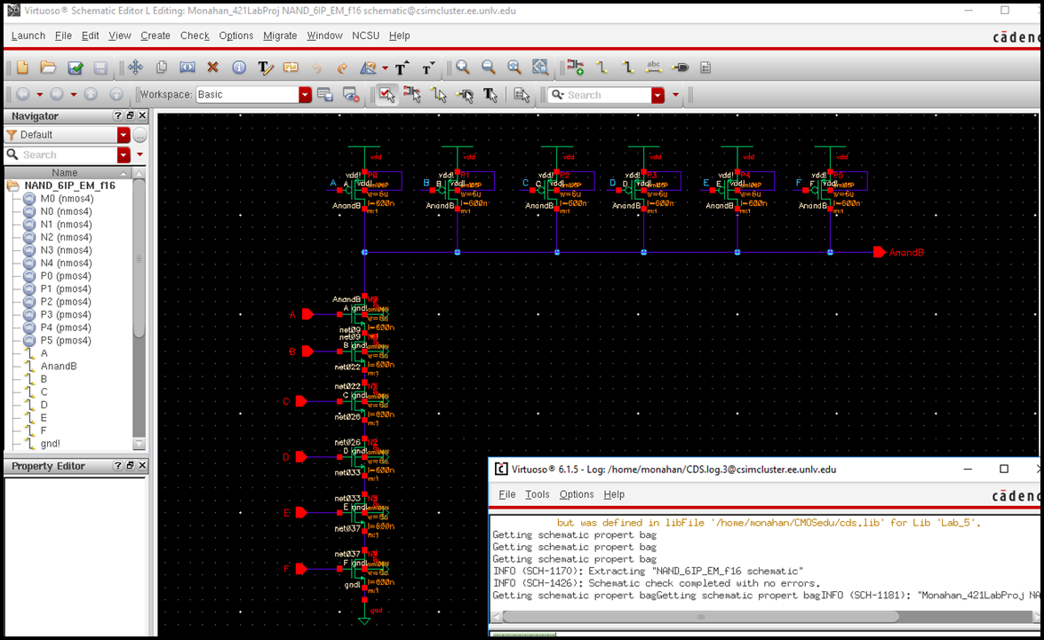
has detected the proper sequence, 101011. The 6-input NAND schematic with DRC
verification is displayed below. These files can be found in NAND_6IP_EM_f16.

After designing the schematic, the
symbol, displayed below, was drafted.

Next, the 6-input NAND gate was
simulated to verify proper design and functionality. The simulation schematic
and results are displayed below. These files can be found in NAND_sim_6IP_EM_f16. Note the gate
works as intended, with the output AnandB going low
when all inputs are high and going high whenever a single input is low.
Additionally, in preparation for the final circuit, note the logic sequence
starting at 20.0ns reads 101011 from A to F with the output high. This
demonstrates the gate will output the proper detection signal once the sequence
is read.


After the NAND gate was drafted, the
detection circuit was finally drafted. The circuit schematic with DRC verification
is displayed below. These files can be found in Detect_Circuit_EM_f16.

Following, the circuit symbol was
drafted. Note, the circuit has inputs labeled 'in' and
'clk' and output 'detect'. The detector circuit
symbol is displayed below.

Next, the circuit was tested to
determine if the serial input 101011 will result in a logic high at the detect
output and all other sequences result in a logic zero. To implement the proper
sequence, two pulse generators were used on the input 'in'. The pulse
generators are each connected to a diode to prevent the voltage sources from
feeding into each other. To ensure an output high of 5V, the pulses were set to
5.7V to compensate for the drop across the diode. The first pulse, below left,
was set to ensure the first 5 elements of the sequence, '10101'. The clock,
below right was set with a slight delay to ensure the output of the input from
the first pulse source. To ensure the last part of the sequence was the
required '1', the second pulse, below center, was set with a delay that would
rise just when the first pulse would fall to zero, resulting in the clock
seeing a logic high on the sixth positive edge. The net result was the first
sequence read by the detect circuit was 101011.


Finally, the detect circuit was
simulated. These files can be found in Detect_Circuit_sim_EM_f16.
The simulation schematic using the circuit symbol is displayed below.

The simulation results are displayed
below. Note the proper sequence has been input with the output,
'detect' remaining low, until the sequence is exact. Once the sequence is
101011 on the sixth positive edge, the NAND receives logic high signals and
sends out a low signal that passes through the inverter and finally, 'detect'
sends out a logic high denoting the given sequence has been detected. On the
next positive edge, the sequence changes and the output 'detect' goes low for
the remaining inputs.

To further ensure the circuit works
as designed, the clock was delayed a little longer to simulate different sequences.
This simulation can be found in Detect_Circuit_sim2_EM_f16.
As seen below, 'detect' is always low for sequences other
than 101011.

2.
Second half of the project, a verified layout and documention
(in html), is due at the beginning of lab on Nov. 30.
Put
your report in the /proj folder in your
directory at CMOSedu.
The second part of the project
requires a layout for the Detector Circuit. The images below display the DFF
layout with DRC verification found in ET_DFF_EM_f16.


Next, the DFF extracted view with LVS
verifications are displayed below.


To simplify the layout for the final detect
circuit, a 12/6 transmission gate(TG) layout was
created. The transmission gate layout with DRC verification is displayed below.
The TG file is titled TG_12_6_EM_f16.

The extracted TG with LVS
verification is displayed below.

Next, the 12/6 inverter layout was
completed. The layout with DRC verification found in file inv_12_6_EM_f16 is displayed below.

The inverter extracted view with LVS
verification is displayed below.

The next component completed was the
6-input NAND gate. The layout and DRC verification found in file NAND_6IP_EM_f16 are displayed below.


The extracted 6-input NAND with LVS
verification is displayed below.

Finally, the detect circuit layout
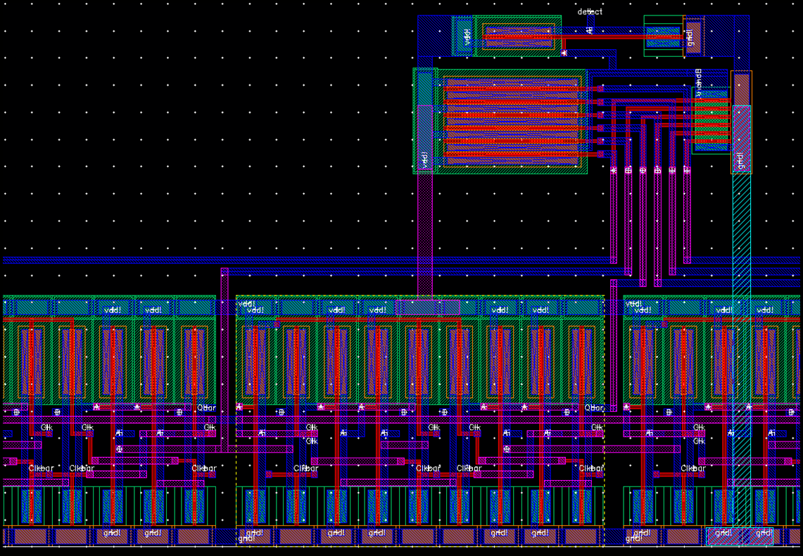
was created with successful DRC verification. First, an expanded view of the
entire layout with DRC verification is displayed below. The reference file is
titled Detect_Circuit_EM_f16.

Next, a closer view of the DFF connections
to the 6-input NAND and inverter out of the NAND is displayed below.

The DFF input's to the NAND will now
be displayed sequentially to demonstrate the connection order resulting in the
detect circuit properly detecting the sequence '101011'. The sequence starts on
the right end of the expanded view displayed earlier.


The 3 images displayed above confirm
the layout view properly connects the 6 DFF's to the 6-input NAND for the given
sequence. The final step of the design was to extract the circuit and obtain LVS
verification. The resulting detect circuit extracted
view with successful LVS verification is displayed below.

Ensure
that there is a link on your project report webpage to your zipped design
directory.
EE421L
Project Design Directory
Return to
Monahan Lab Report Directory
Return to EE 421L
Fall 2016 Student Directory