Lab 6 - ECE 421L
For this prelab 6 we went through Tutorial 4 for the cadence design system from CMOSedu.com.
There we constructed schematics, simulated, and then did the
layouts for a NAND gate. Just a side note, components from
Tutorial 3 were used initially to save time and for convenience in
gathering components for this preLab.
I. NAND gate:
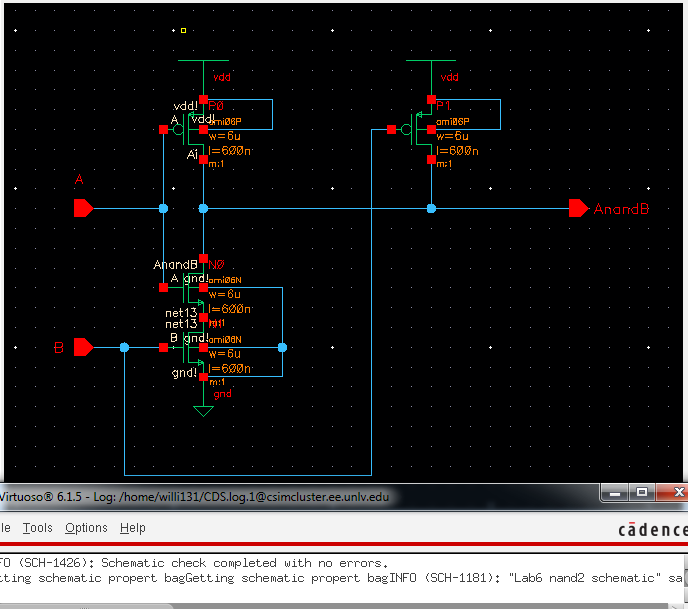
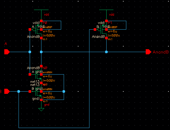
a. First, as mentioned above, we copied our inverters from our previous tutorial library.
b. Then we rerouted wiring and rearranged our components to create our NAND gate seen below:
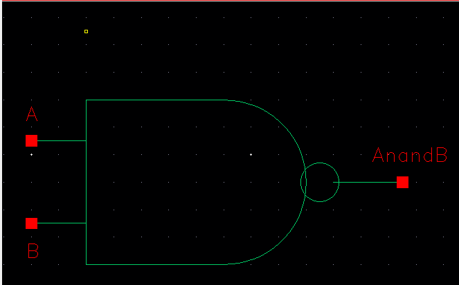
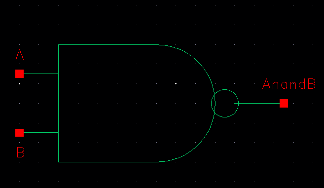
d. Then, after our symbol was created and saved with no errors I opened up another schematic environment and instantiating my symbol constructed another schematic to use for simulation. Below you can see the two inputs and an output with a capacitative load.
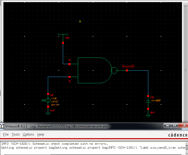
Above here, you can see that it was checked and saved with no errors...
II. Simulations
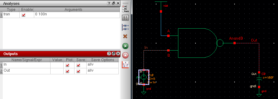
a. From our schematic above, we launch the ADE L to set everything up and simulate.
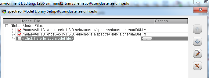
b. In order for us to run our sim, we had to redirect to our model libraries which include our nmos and pmos devices.
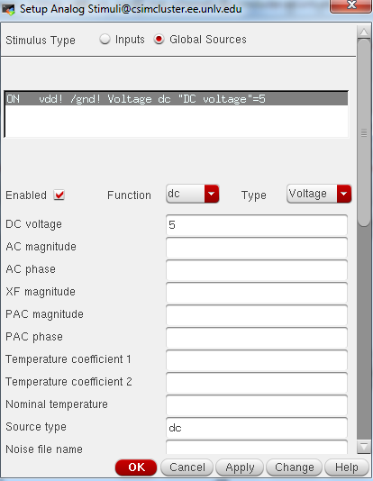
c. Below you can see the libraries as well as the set up for our stimuli variable.
d. Finally, setting up our transient analysis and selecting our simulation outputs (directly from schematic) we run our simulation.
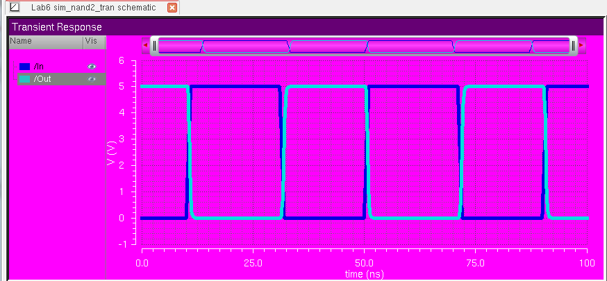
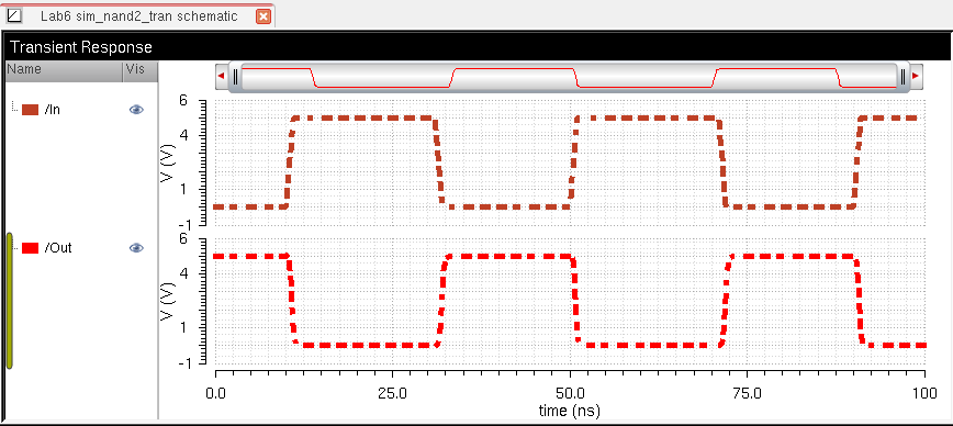
e. Below is my output of my NAND gate. Because it may possibly be a little difficult to see my input and output very clearly, I seperated the two signals just below for a better visual.
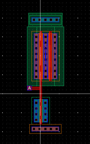
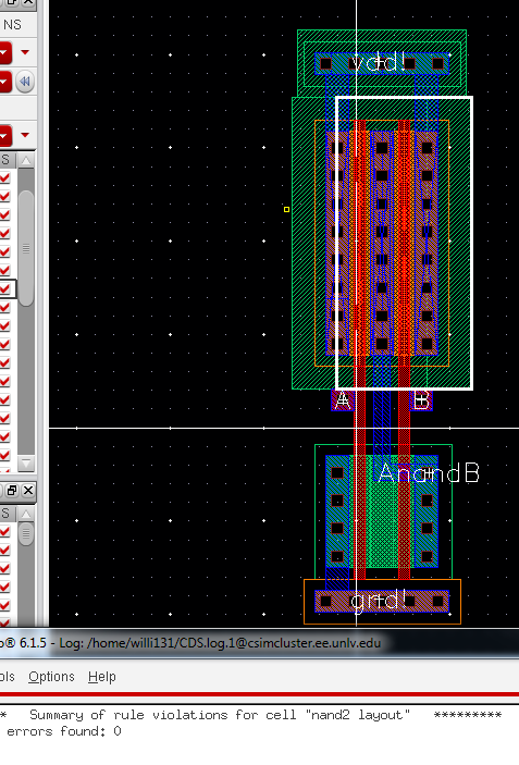
III. Layout
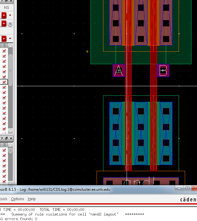
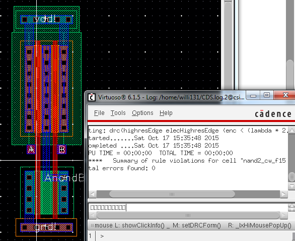
A. Below is the layout of my NAND gate. The next few screen shots show the different steps into constructing it. For the most part, we simply instantiated the components to be used...
 w
w
*Though it's probably no necessary to show here, but I DRC-ed my layout several different times as I went just to ensure everything was good..
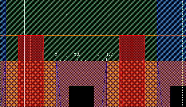
b. Below you can see the ruler that was brought out due to a path issue for our width.
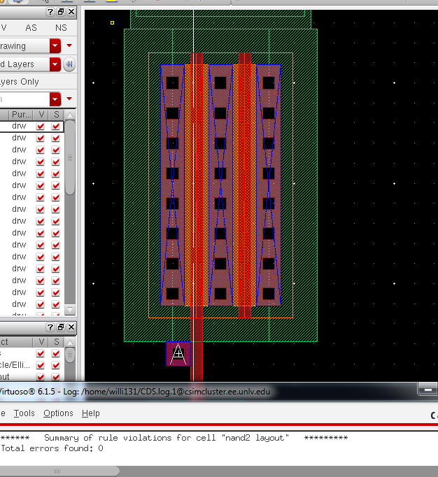
C. DRC was ran successfully with no errors as shown below:
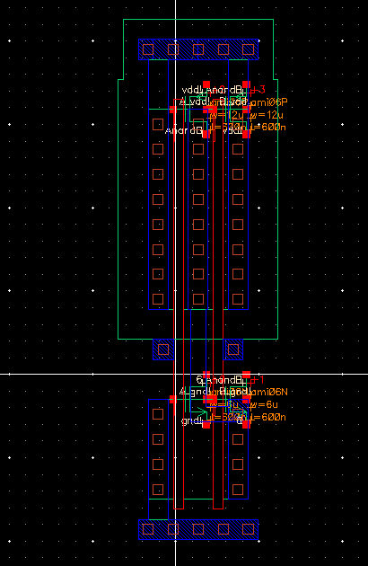
d. finally, we extracted our layout with the result shown here:
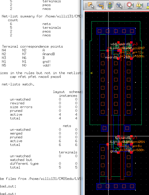
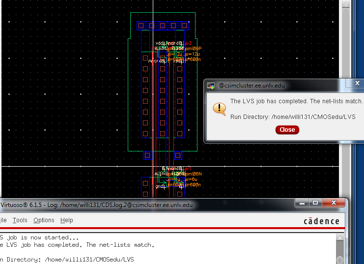
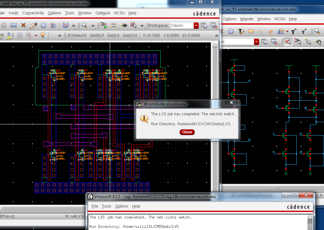
e. Finally, an LVS was ran with our simulation schematic and extracted layouts successfully with matching netlist results.
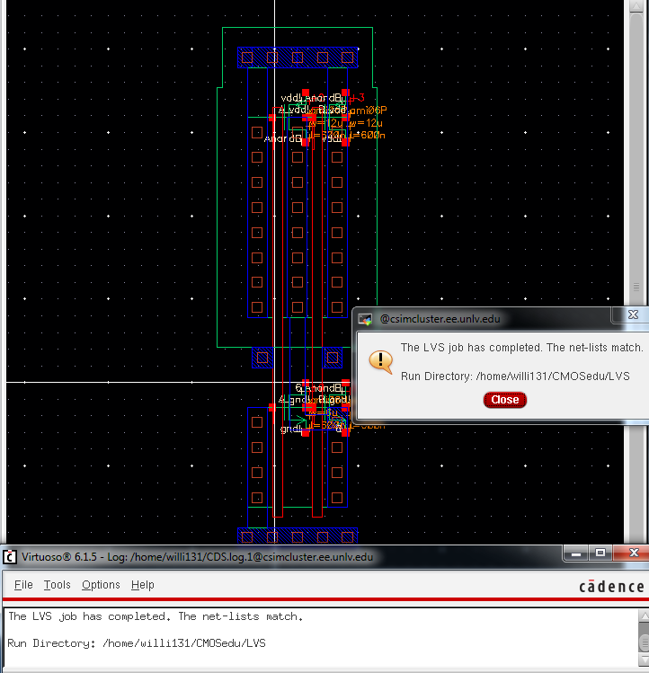
Here is a look at the resulting net-list:
All files were backed up for this prelab and emailed/saved on a flash drive.
POST LAB 6 REPORT:
For this lab we constructed the 2-input XOR gate, tested to observe behavior, created layout, and symbol, and then along with our 2-input NAND gate created in the prelab above, we put them together to build an ADDER. For the ADDER we created a symbol, simulated it to see its behavior, and then created the layout for it using Cadence.
I. NAND GATE:
First the NAND gate was constructed using NMOS and PMOS transistors. For this lab we used 6/.6um of both components... Below you can see the schematic built.
Next, a symbol for the NAND gate was made that will be later used in a schematic for a simpler view.
Finally, the layout was created. Below you can see the NAND gate layout with a successful DRC for no errors...
II. XOR GATE:
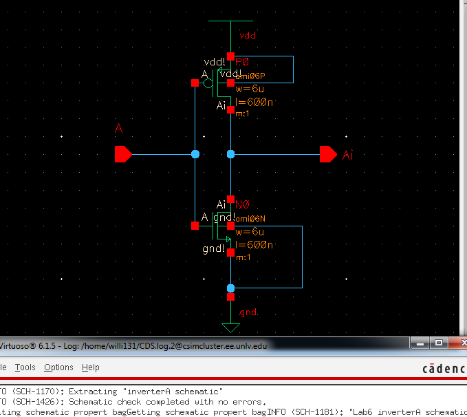
Next, the XOR Gate was created. Below is the schematic (in progress) of an XOR gate created using the PMOS and NMOS transistors. You'll notice that two inverters were used in the building of the gate. The PMOS transistors were corrected from the 12/.6 um used previously to the same size as the NMOS transistors of the 6/.6um in the final schematic.
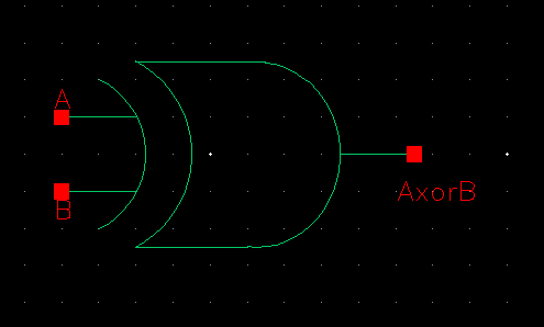
Below is the symbol I made for the XOR gate.
After the DRC returned no errors for my layout it was then extracted as seen below...
With the extracted view, LVS was ran successfully with a matching net-list for the schematic of the XOR gate shown previously.
III. TESTING GATES:
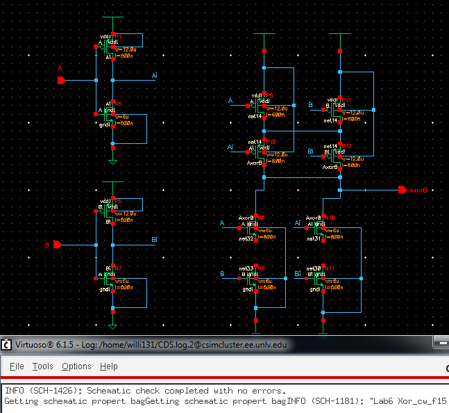
Now, before we can continue and construct the full adder, we need to take a look at all our gates to be used in order to ensure proper operation. Below is a test circuit constructed with one of each of my gates I created (Inverter, NAND, and XOR).
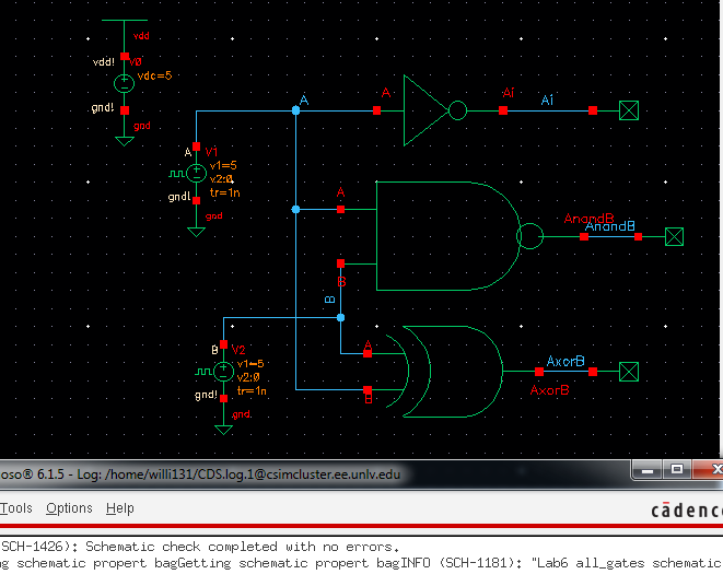
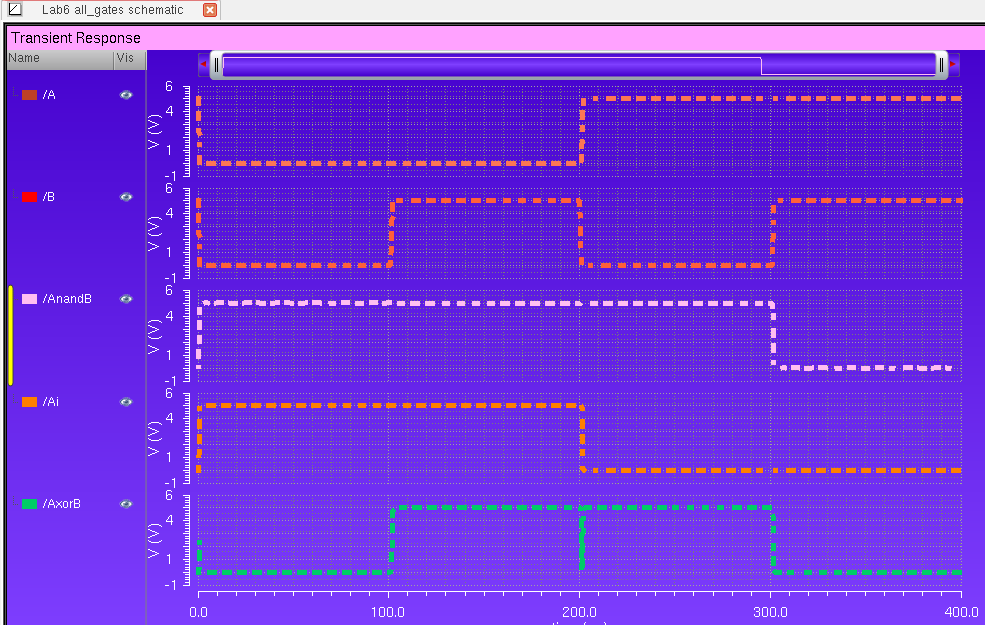
After ensuring that my circuit was saved with no errors (seen above), I opened the ADE L to run the transient analysis. Below you can see the resulting outputs from the simulation of the ciruit above. The first two are my inputs, A & B to show what is going into each gate...
Output AnandB- NAND gate output acting as expected, high when one or both inputs are low, and then low with both inputs are high.
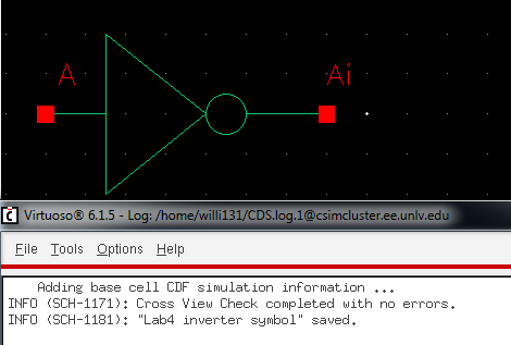
Output Ai- Invertor shown above only has one input, that's input-A. So you can see that when input-A is low, the output of the invertor is high. And then naturally as you'd expect an invertor to do, when the input goes high, theoutput goes low.
Output AxorB- XOR gate output shows with the two inputs, A & B, when both inputs are low or both are high, the output of the XOR gate is low. Then, if only one of the inputs are high or low, the XOR gate output goes to high.
*** You'll notice a glitch in the XOR input when the both inputs are switching, (A goes from low to high and B goes from high to low) Because gates are not able to switch instantaneously, there is a tiny bit of a delay. This causes the little glitch in our output. However, it is quickly corrected once the switching is complete and a steady state is reached again.***
IV. FULL ADDER:
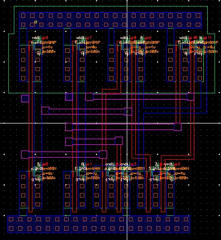
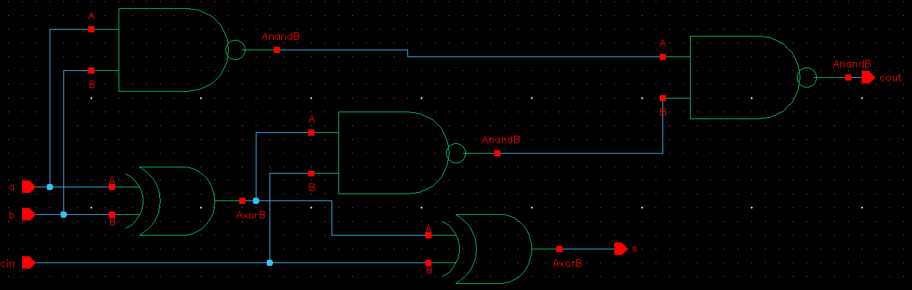
Now that each gate's operation has been verified to properly run it is time to construct the full-adder using each of the already discussed components above. Below you can see the schematic for the full adder. Here we use the NAND and XOR gates to build the adder. Keep in mind that the inverter is included within the gates so they are shown in the schematic below.
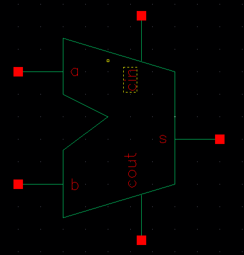
After constructing the above circuit, a symbol for the ADDER was created, seen below.
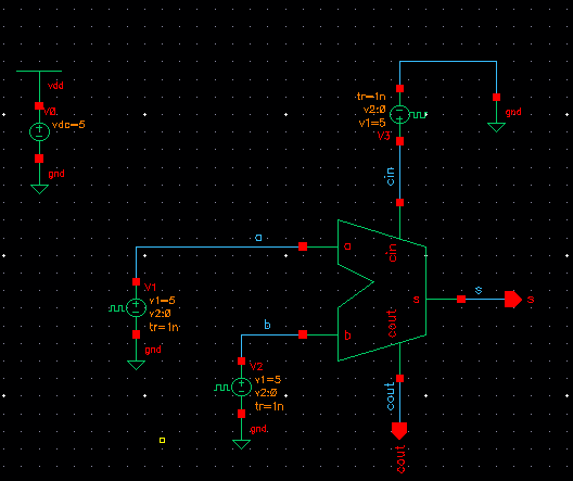
Next, of course we need to test our schematic for proper operation. Below is a test circuit using just the symbol from above (which is encompassing of the schematic just shown as well).
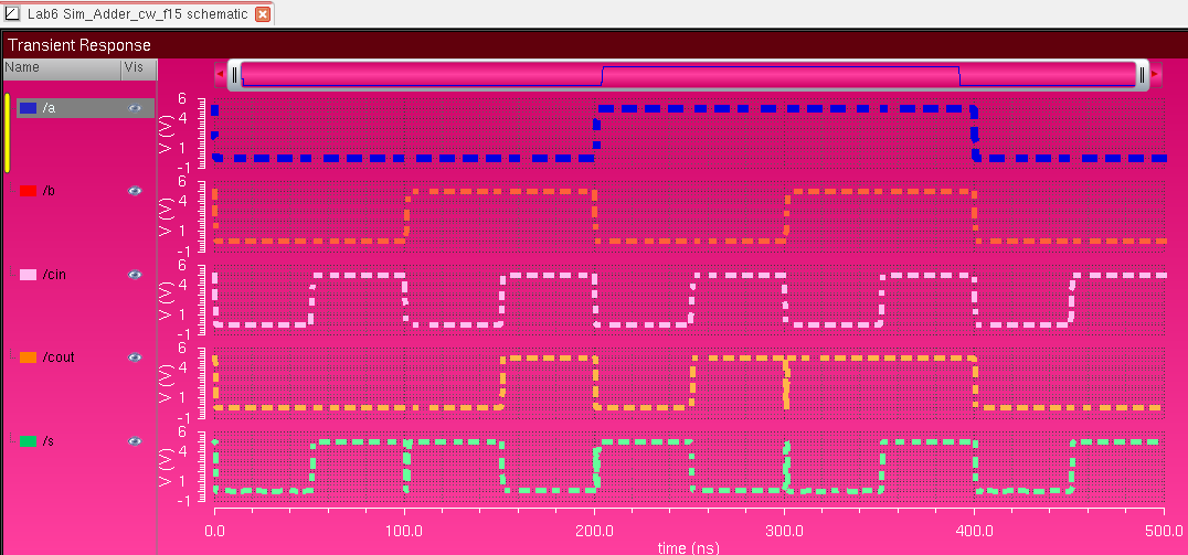
Below is transient response from the above circuit.... Now here, you can see that in the Cout and S Outputs there is that glitch again. This is caused once again by the XOR gate and the switching of the inputs. Below you can see that the ADDER is behaving just as expected: Adding the inputs 0+0=0, 0+1=1, 1+0=1, 1+1=1 (with a carry out...), and so forth.
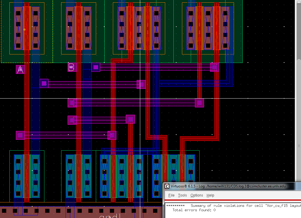
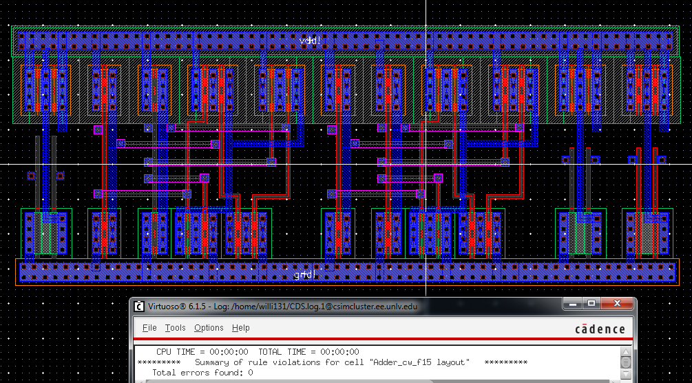
Finally, The layout was created for the full adder. Shown below, I layed out a NAND gate, the two XOR gates, and then the last twon NAND gates side by side and connected them up to correspond with the schematic. As I moved along building my layout I continuously DRC-ed it to ensure no design violations were found and if there were any it would be easy to find...
Below is my final Layout. :)
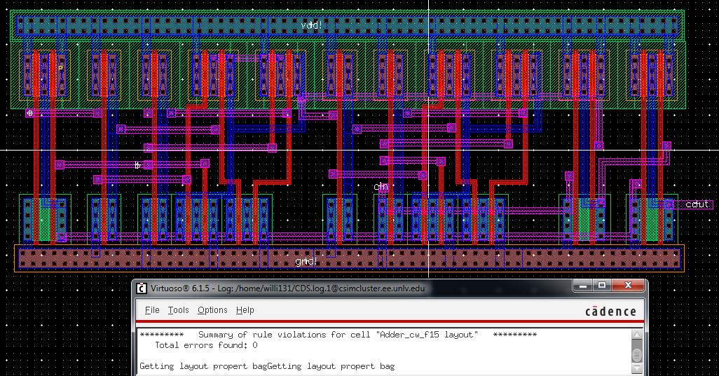
After ensuring the final ADDER layout DRC-ed successfully, I once again extracted the layout as shown below.
V. ISSUES
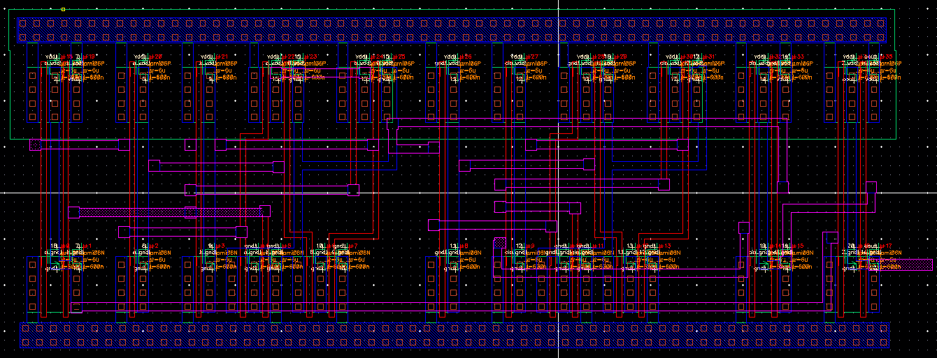
So after I extracted the layout I ran the LVS. This was unsuccessful and there were many errors found. I went through and corrected many of them which were numbers of nets that were different between the schematic and the layout, some naming issues, output/input pin variances, etc.... After completing these, I was able to clear many errors however the LVS still returned with non-matching netlists. A reason this might be could be caused from me flattening my NAND gates in order to modify them to the 6/.6um sizes for the PMOS'. Originally when they were constructed in the prelab the PMOS transistors were 12/.6um. In my attempt to correct/over correct my layout cellview ended up getting deleted :'(. Due to time I was unable to rebuild my ADDER layout and get the LVS ran. This is something that will be remedied this week though. I will have to start from scratch and resize my transistors before copying the layout symbols as it should help eliminate the need to flatten the layers for modification in the layout itself. I think I just made it more complicated than it needed to be. This will be updated as soon as I am able to rebuild and LVS my adder again.
VI. Backup
All files were backed up on flashdrive and emailed to myself.