Lab 5 - ECE 421L 

Cassandra Williams

Willi131@unlv.nevada.edu

September 28, 2015


PreLab: 

 This Prelab takes us through Tutorial 3 of  Cadence from the CMOSedu.com website.  In this tutorial we create the schematic, symbol, and layout of a CMOS interverter.  Then we simulate both the schematic and extracted layout to see how the inverter behaves.

A.  Inverter 

    1. First, we build our inverter schematic.  Here because we have done the previous tutorials (shown in previous labs) we can simply copy and past our NMOS and PMOS devices into the schematic.  They were already the needed sizes.  Then we just wire it up as shown below adding our A-input pin and Ai-output pin.  

        a. You can see the arrangement of components I have as PMOS on top and the NMOS on the bottom.  Because the body of the PMOS is connected to VDD and the body and source of our NMOS are connected to ground this form makes the most sense.... We have our NMOS drain connected up to the PMOS drain.

http://cmosedu.com/jbaker/courses/ee421L/f15/students/willi131/Lab%205/PreLab%20Pics/1.%20Schematic.PNGhttp://cmosedu.com/jbaker/courses/ee421L/f15/students/willi131/Lab%205/Lab%20Pics/1.%20Schematic.PNG


     b. Next, I created the symbol for my inverter shown below.  This is encompassing of the schematic above.  As you can see at the bottom of each snip, my schematic and symbol were both checked and saved with no errors.


http://cmosedu.com/jbaker/courses/ee421L/f15/students/willi131/Lab%205/Lab%20Pics/2.%20Inverter%20Symbol.PNG


     c.  After getting those two things completed, I created a layout of my inverter.  Here, instantiating ntap, PMOS, ptap, and NMOS I layed it out just as shown in the schematic.  My connections were made with the poly and metal1.  The DRC results shown at the bottom of my layout were successful with no errors.  Next to my layout you can see the skeleton layout of the devices and my connections.  There you can clearly identify the gate (poly), drain, and source (metal1) of each device.


http://cmosedu.com/jbaker/courses/ee421L/f15/students/willi131/Lab%205/Lab%20Pics/3.%20Inverter%20Layout%20DRC_a.PNG                     http://cmosedu.com/jbaker/courses/ee421L/f15/students/willi131/Lab%205/Lab%20Pics/4.%20Zero%20stop_Show%20Wiring.PNG


     d.  Next, I created my pins for each connection vdd!, A, Ai, and gnd!.  * '!' declaring global*  Then I DRC-ed just to make sure everything was still good and it returned successful with no errrors.


http://cmosedu.com/jbaker/courses/ee421L/f15/students/willi131/Lab%205/Lab%20Pics/5.%20Final%20Inverter%20DRC_b.PNG


    e.  After my layout was complete, I extracted it.  Then, opened the extracted layout from the Cellview library.  Below shows the extracted layout.  After I got this opened up I ran an LVS with my schematic I originally constructed.   LVS was successful with netlists matching!


http://cmosedu.com/jbaker/courses/ee421L/f15/students/willi131/Lab%205/Lab%20Pics/6.%20Extracted.PNG                            http://cmosedu.com/jbaker/courses/ee421L/f15/students/willi131/Lab%205/Lab%20Pics/7.%20LVS%20good.PNG


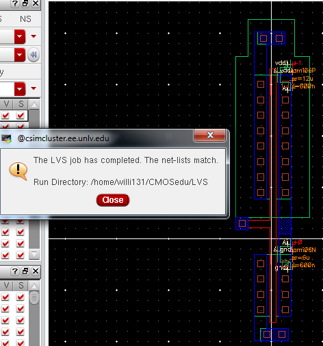
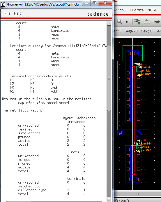
Below is the netlist output of the LVS to show nets did indeed successfully match.

http://cmosedu.com/jbaker/courses/ee421L/f15/students/willi131/Lab%205/Lab%20Pics/8.%20LVS%20Output_b.PNG


     f.  Next, I created a new schematic using my interter symbol created simply by instantiating my symbol in and wiring up and labeling in/outputs. This too was saved and checked with no errors.


http://cmosedu.com/jbaker/courses/ee421L/f15/students/willi131/Lab%205/Lab%20Pics/9.%20Sim%20Schematic.PNG


   g.   Next, to see how the inverter behaves we ran a DC analysis shown below.  Here, I had my voltage source going from 0V to 5V in 1ms steps.  I selected my outputs to be plotted directly on the schematic.


http://cmosedu.com/jbaker/courses/ee421L/f15/students/willi131/Lab%205/Lab%20Pics/9b.%20Analysis_a.PNG


  Below are my simulation results:


   You should notice here that my Vout is at zero no matter the Vin voltage level.  This is due to there not being any driving voltage turning the inverter actually on!

http://cmosedu.com/jbaker/courses/ee421L/f15/students/willi131/Lab%205/Lab%20Pics/10.%20Sim%20Inverter%20Output_a.PNG


   To correct this, we added the vdd net to the schematic.  This gives in symbol vdd the voltage signal for it to be on.


http://cmosedu.com/jbaker/courses/ee421L/f15/students/willi131/Lab%205/Lab%20Pics/11.%20Sim%20Inverter%20Correction_b.PNG


   After adding the vdd net source to the schematic above, I re-ran the simulation.  Below you can see the results.  Now you can get a good idea of how the inverter behaves....  As the Vin goes up from 0V to 5v, you see the Vout voltage run in the opposite direction, starting up at the 5V and dropping down to 0V.  This in summary shows an inverter 'inverts" the input voltage to the output.


http://cmosedu.com/jbaker/courses/ee421L/f15/students/willi131/Lab%205/Lab%20Pics/12.%20Sim%20Inverter%20Correct%20Output_b.PNG


Next, just to ensure that my layout will behave in the same way as the schematic, I ran a simulation of the extracted layout...  Below is the output (same as above) and the netlist where you can see that the extracted layout was indeed simulated.


http://cmosedu.com/jbaker/courses/ee421L/f15/students/willi131/Lab%205/Lab%20Pics/13.%20Extracted%20Sim%20Netlist%20End.PNG


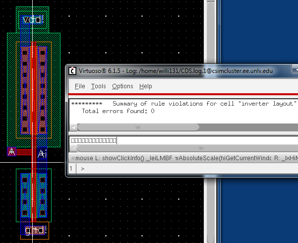
All Files and snips were saved and backed up via email and flashdrive.


______________________________________________________________________________________________________________________________________________

______________________________________________________________________________________________________________________________________________


Lab 5 Report:


   For this lab we draft schematics, layouts, and symbols for two different sized inverters.  The first one is a 12u/.6u PMOS and a 6u/.6u NMOS (where our m=1) and the next uses both 48u/24u device (with our m=4).  Here we'll simulate and see how an inverter works and behaves with various load capacitances.


I.  Schematics/Layouts


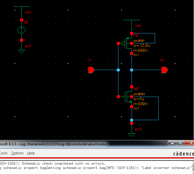
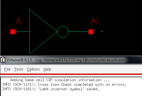
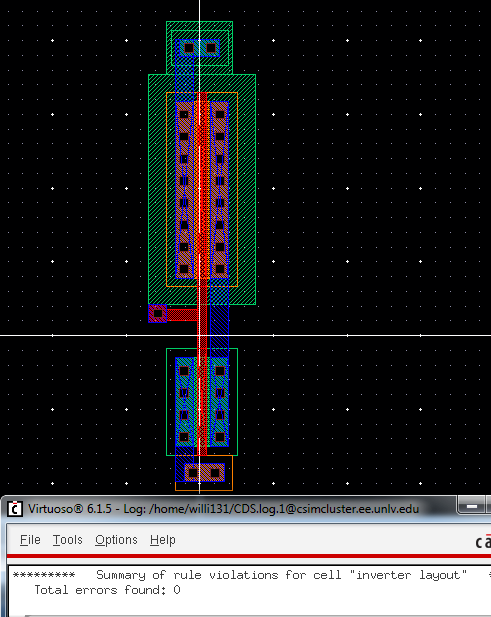
   A.  For the small inverter the schematic, symbol, and layout are shown above.(See Prelab portion)  

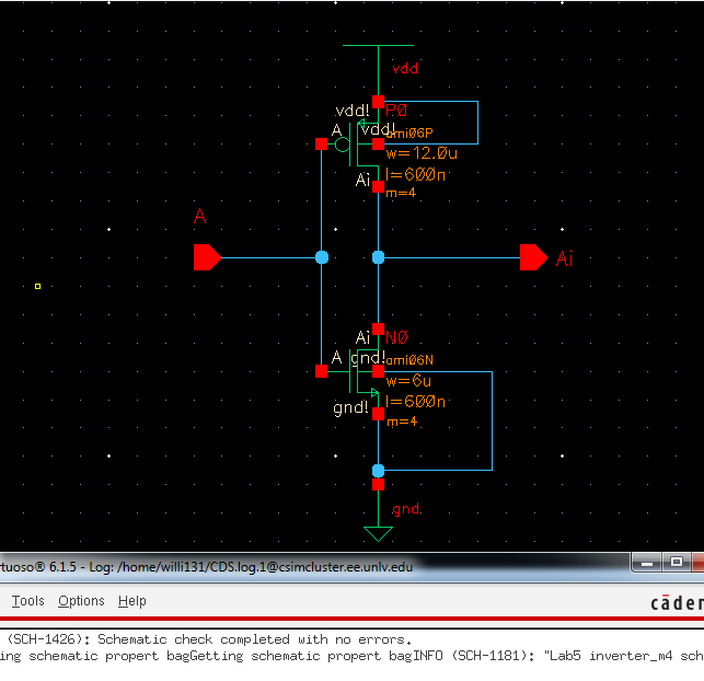
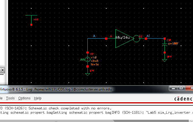
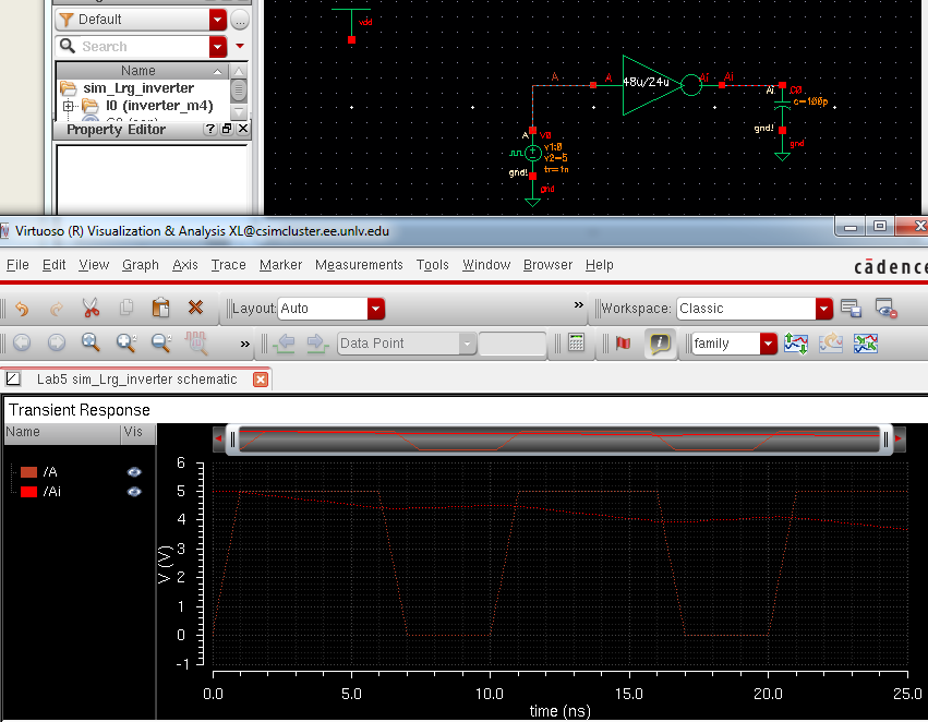
   B.   Our large inverter is shown below in the schematic.  As you can see, the m (multiplier) is set to 4.  *Please note that the schematic for the small inverter for (A.) is the same only our multiplier is equal to 1.  You can see this above.*


       1. To construct the schematic below, I simply copied and pasted my orginal small inverter into the schematic window.  Then modified each by selecting and pressing "Q" to edit the device and change the m to equal 4.


http://cmosedu.com/jbaker/courses/ee421L/f15/students/willi131/Lab%205/Lab%20Pics/PostLab5/1.%20m4%20Inverter%20Schematic.PNG


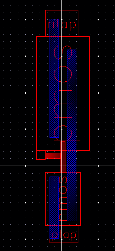
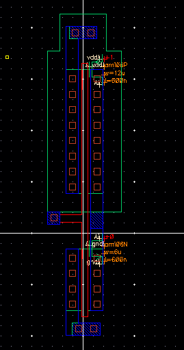
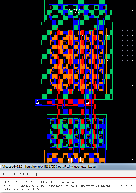
     C.  After saving and checking with no errors found in my schematic, I created a new cellview and opened the Layout window.  Here I simply copied my original layout from the small inverter in the prelab and pasted it here.  Then, modifying the layout to match my multiplier (m=4) I got the following result seen below.
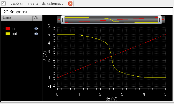
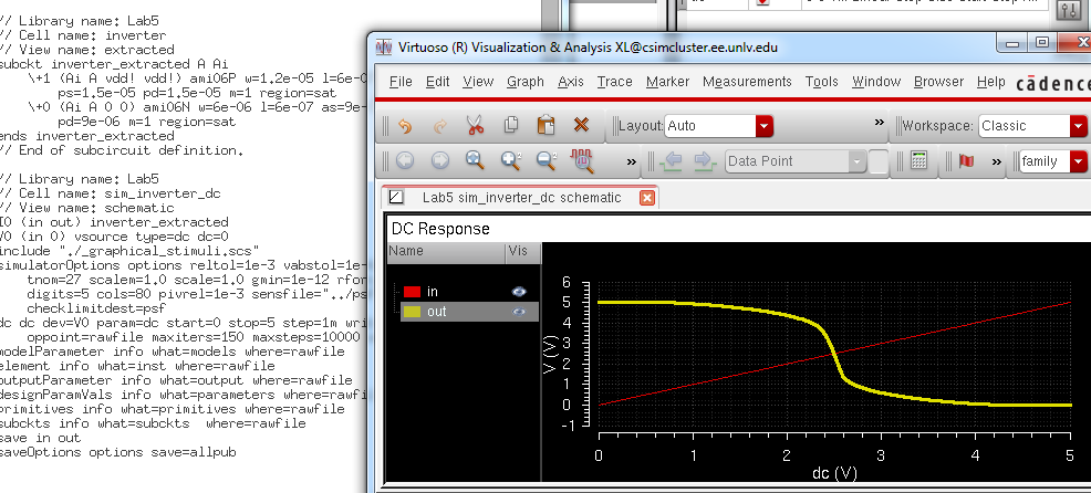
http://cmosedu.com/jbaker/courses/ee421L/f15/students/willi131/Lab%205/Lab%20Pics/PostLab5/2.%20m4%20Inverter%20Layout_DRC.PNG


II.  Simulations:


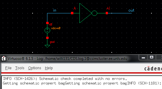
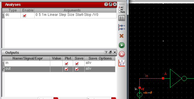
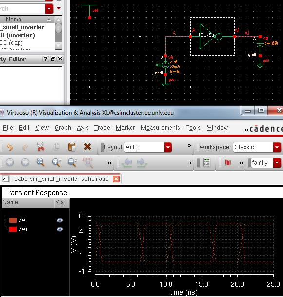
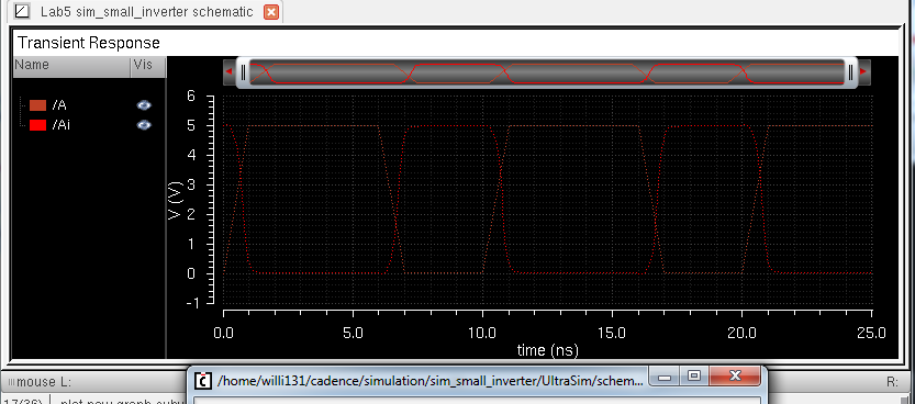
     A.  Below, using my small inverter symbol (seen in schematic and originally constructed in the prelab), I built my simulation schematic. 


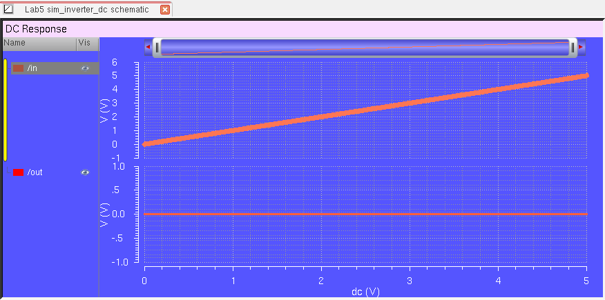
         1.  The first simulation was using a 100 fF capacitor.  Here you can see the output (Ai) is pulsing just as the input only in an inverted fashion.

               http://cmosedu.com/jbaker/courses/ee421L/f15/students/willi131/Lab%205/Lab%20Pics/PostLab5/3.%20m1%20Inverter%20sim%20100fF.PNG


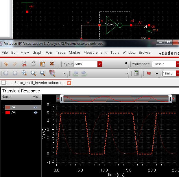
           2.  Next, simulation was with a 1pF capacitor. (Capacitances simply changed by selecting cap and hitting "Q" to edit)


               http://cmosedu.com/jbaker/courses/ee421L/f15/students/willi131/Lab%205/Lab%20Pics/PostLab5/4.%20m1%20Inverter%20sim%201pF.PNG


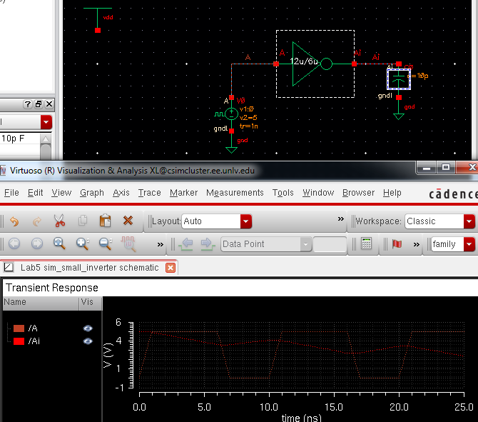
           3. Simulation of inverter with a 10pF capacitor:  You can see that our ourput voltage is beginning to steady out with the increase capacitor value....

                http://cmosedu.com/jbaker/courses/ee421L/f15/students/willi131/Lab%205/Lab%20Pics/PostLab5/5.%20m1%20Inverter%20sim%2010pF.PNG


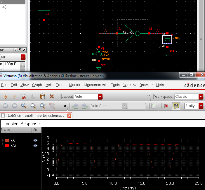
           4.  Inverter with 100pF capacitor:   Here you'll notice very little variation in our output!

                 http://cmosedu.com/jbaker/courses/ee421L/f15/students/willi131/Lab%205/Lab%20Pics/PostLab5/6.%20m1%20Inverter%20sim%20100pF.PNG


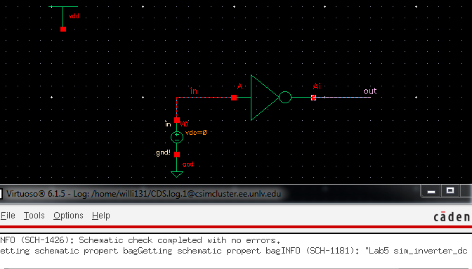
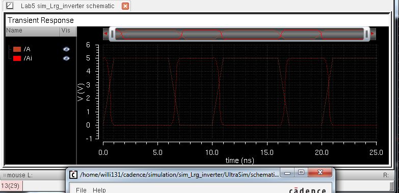
     B. Now we have our simulations of our large inverter...


         1.  First, you will notice that my inverter symbol is now of the m=4 inverter (48u/24u). This schematic was checked and saved with no errors before launching the ADE L and repeating simulations seen above in part A for the small inverter.

              http://cmosedu.com/jbaker/courses/ee421L/f15/students/willi131/Lab%205/Lab%20Pics/PostLab5/7.%20m4%20Inverter%20S&C.PNG


           2.  Large Inverter with 100 fF cap:

              http://cmosedu.com/jbaker/courses/ee421L/f15/students/willi131/Lab%205/Lab%20Pics/PostLab5/8.%20m4%20Inverter%20sim%20100fF.PNG

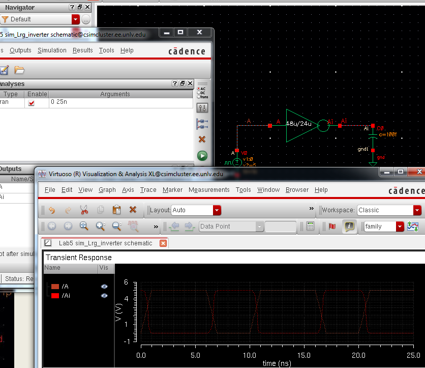
              Above you can see that our simulation results are just like the first simulation with the 100fF capacitor of the small inverter.


        3.  Next up is the 1pF simulation...
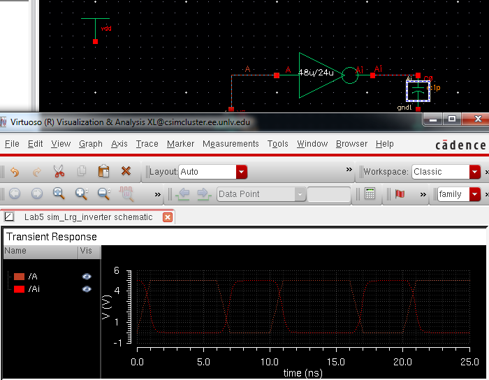
  

                http://cmosedu.com/jbaker/courses/ee421L/f15/students/willi131/Lab%205/Lab%20Pics/PostLab5/9.%20m4%20Inverter%20sim%201pF.PNG

                 *Notice a pattern?*


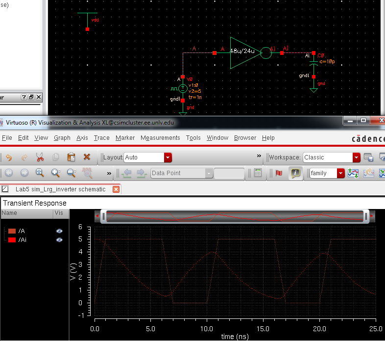
            4.  Below is the 10pF capacitor simulation:


                http://cmosedu.com/jbaker/courses/ee421L/f15/students/willi131/Lab%205/Lab%20Pics/PostLab5/10.%20m4%20Inverter%20sim%2010pF.PNG


          5.  And finally our 100pF capacitor... Here you can see that the output voltage becomes less and less varying as the capacitance goes up just as seen before.

              http://cmosedu.com/jbaker/courses/ee421L/f15/students/willi131/Lab%205/Lab%20Pics/PostLab5/11.%20m4%20Inverter%20sim%20100pF.PNG


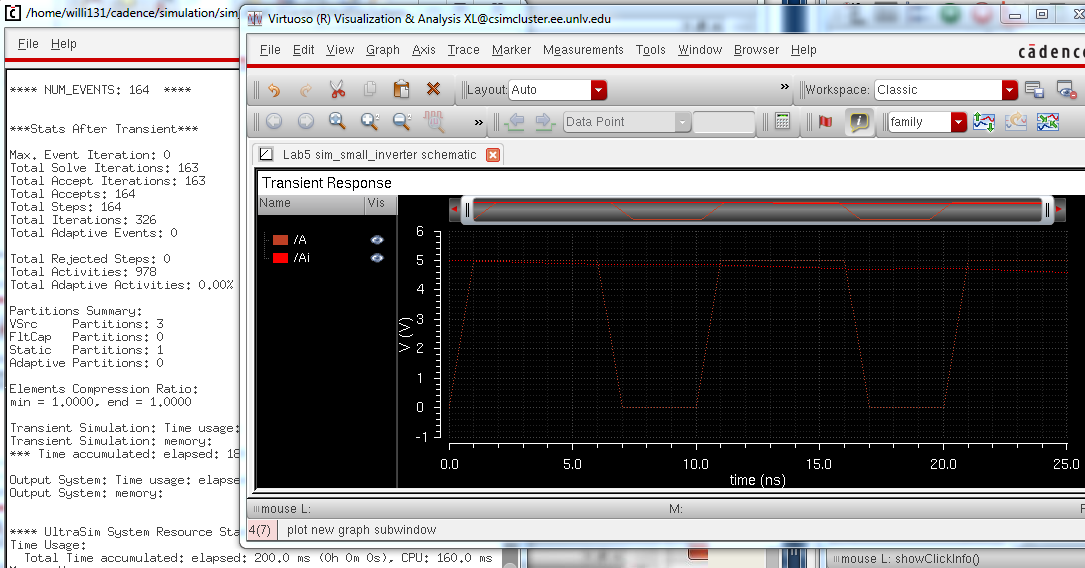
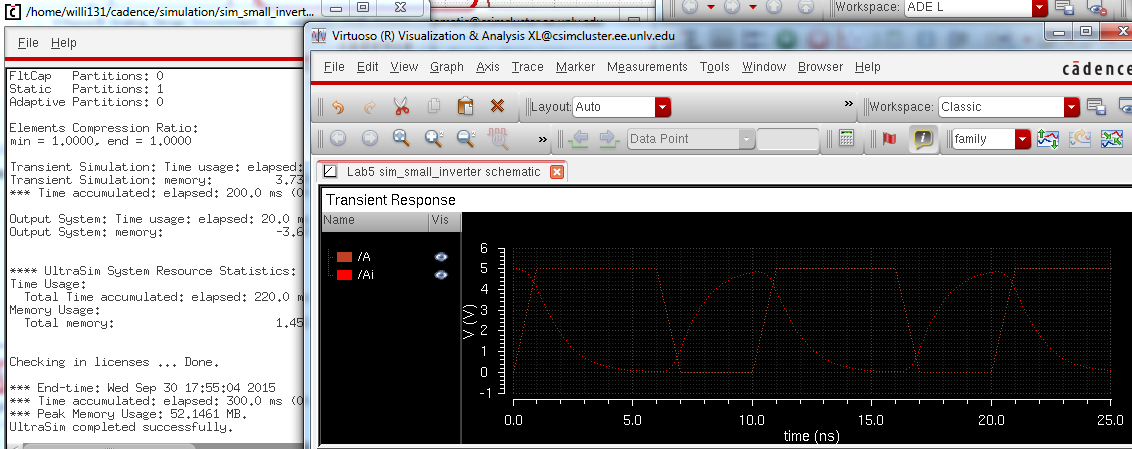
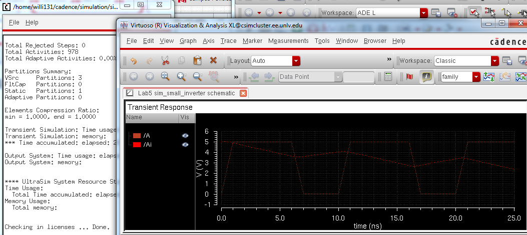
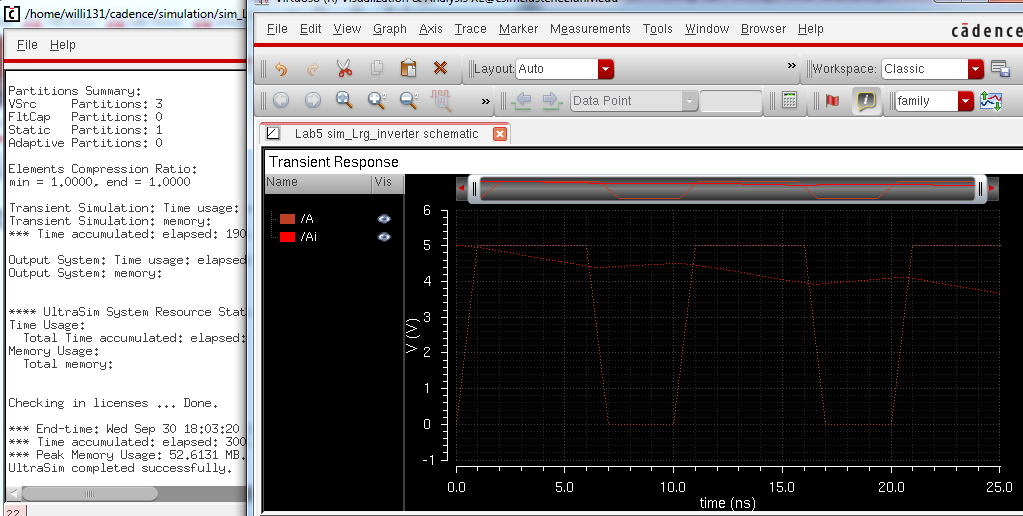
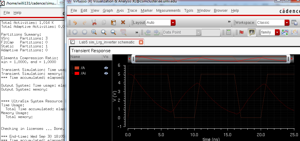
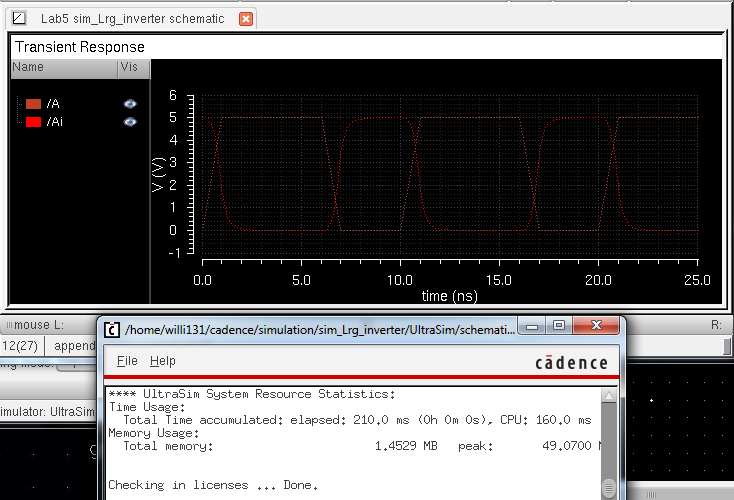
     C.  The last part of the lab was resimulating our schematics above with the different sized capacitors using the Ultrasim function. Ultrasim is useful when you have a large schematic to simulate and need to complete it in a timely manner, however it is not as accurate as spectre.  
   
     
            1.  Small inverter:  100pF Capacitor:

                    http://cmosedu.com/jbaker/courses/ee421L/f15/students/willi131/Lab%205/Lab%20Pics/PostLab5/12.%20m1%20Inverter%20ultrasim%20100pF.PNG


       2.  Small inverter:  1pF capacitor:


http://cmosedu.com/jbaker/courses/ee421L/f15/students/willi131/Lab%205/Lab%20Pics/PostLab5/13.%20m1%20Inverter%20Ultrasim%201pF.PNG


       3.  Small Inverter:  10pF capacitor:

http://cmosedu.com/jbaker/courses/ee421L/f15/students/willi131/Lab%205/Lab%20Pics/PostLab5/14.%20m1%20Inverter%20Ultrasim%2010pF.PNG


         4.  Then finally, the small inverter using the 100fF capacitor:


http://cmosedu.com/jbaker/courses/ee421L/f15/students/willi131/Lab%205/Lab%20Pics/PostLab5/15.%20m1%20Inverter%20Ultrasim%20100fF.PNG


        5.  Here we begin with the large inverter Ultrasim results:  Starting off with the 100 fF cap this time...
   

           http://cmosedu.com/jbaker/courses/ee421L/f15/students/willi131/Lab%205/Lab%20Pics/PostLab5/19.%20m4%20Inverter%20Ultrasim%20100fF.PNG


       6.   Then the 100pF cap:
   

            http://cmosedu.com/jbaker/courses/ee421L/f15/students/willi131/Lab%205/Lab%20Pics/PostLab5/16.%20m4%20Inverter%20Ultrasim%20100pF.PNG


         7.  Large Inverter:  10pF cap:


             http://cmosedu.com/jbaker/courses/ee421L/f15/students/willi131/Lab%205/Lab%20Pics/PostLab5/17.%20m4%20Inverter%20Ultrasim%2010pF.PNG


        8.  Large Inverter:  1pF Cap:


            http://cmosedu.com/jbaker/courses/ee421L/f15/students/willi131/Lab%205/Lab%20Pics/PostLab5/18.%20m4%20Inverter%20Ultrasim%201pF.PNG


   In summary, the simulations showing the behavior of the inverter are pretty much the same between the large and small inverters.  However, the larger inverter seems to switch much quicker than the smaller inverter.  Also, with each change in our capacitor value the results significantly changed.  You can see how the smaller the capacitor, the more sensitive our output was to our input (i.e. pulse input 0V-5V --> pulsing output (chasing/inverted) 0V-5V) actually inverting the signal well.  Then, with each capacitance increase,the longer the delay in the switch and less inverted the signal became.  


    Running the simulations in the Ultrasim didn't bare very different results.  However, you can see a little inacurracy in a couple of the output graphs.  Accuracy is a known trade off for running the Ultrasim.  For this particular experiment, simming such simple schematics didn't make a huge difference.  Perhaps for larger, more complex schematics Ultrasim would be more useful.

   
    Images and files used for this lab can be found here:  lab5_clw.zip

** All files backed up on flashdrive, laptop, and emailed**
http://cmosedu.com/jbaker/courses/ee421L/f15/students/willi131/Lab%205/Lab%20Pics/PostLab5/backup.bmp


Return to Student Lab Reports here.

 
Return to EE 421 Lab website here.