Lab 3 - ECE 421L
Cassandra Williams
Willi131@unlv.nevada.eduSeptember 14, 2015
PreLab:
This Prelab goes through, completing the Tutorial 1 online. Continuing from Lab 1, we take our n-well resistor and create a layout, and then create a layout for our voltage divider circuit created in Lab 1.
I. Voltage Divider Circuit:
First,
beginning where we left off, we modified our voltage divider circuit in
such a way that it is useful in a circuit layout. Here we created
Pins In and Out. These pins will enable us to connect this
circuit to different levels in a layout design in Cadence.
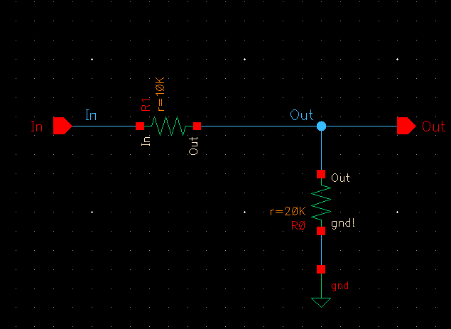
Next, after checking and running the schematic (returning with Zero
errors) we create a symbol to be used in future steps for this circuit.
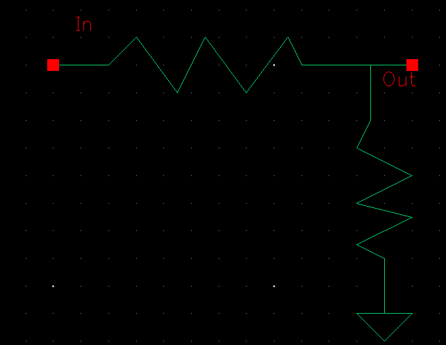
After
creating our symbol, we constructed a new circuit. Utilizing our
above symbol we added a 1V DC source to the input.
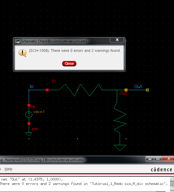
Here
you can see that there are two warnings when saved and checked.
This was due to my floating Output. The warnings were
ignored and rechecked with no errors.
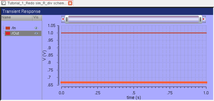
I ran a transient analysis and below are my results:
II. Layout of an 10K n-well Resistor:
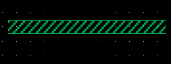
Now
I created a layout of my resistor... Using the C5 process design
requirements of 12*Lambda, here 3.6 microns as lambda is 300nm. I
created a rectangular layout with original width of 4.5um and length of
56um.
With
my laxidaisy drawing, I made my width and length as explained above.
However, when I ran the DRC I received errors shown below...
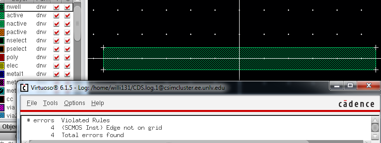
These were remedied by zooming in, moving my rectangle, and
measuring distances from my rectangle to the grid. As my X-Y snap
spacing settings are at .15 microns, this is very little distance
relative to the grid spacing. Next, double checking and making
tiny adjustments to my rectangle size itself, I simply used the formual
of 56/.15= 373.3333... Well, for the layout this number is required to
be a whole number. To correct this I adjusted my lengths to 56.1.
Checking my widths, I was good as 4.5/.15 =30 (A whole number).
After making adjustments and rerunning the DRC I was cleared with
no errors.
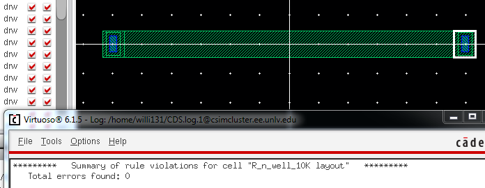
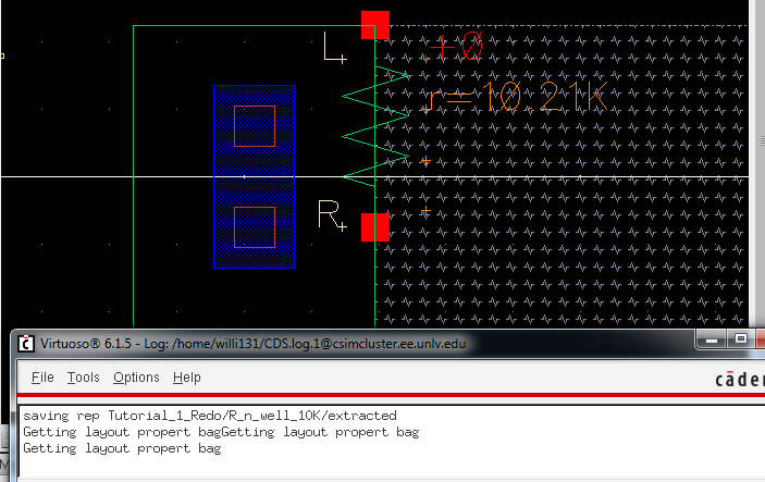
After
geting the n-well tapped and set up as a 10K resister we implemented an
extracted view and confirmed our resistor value.
Next
closed out and created a new layout of Resistor divider
schematic. Using our n-well resistors created previously, built a
layout using two of them as shown below:
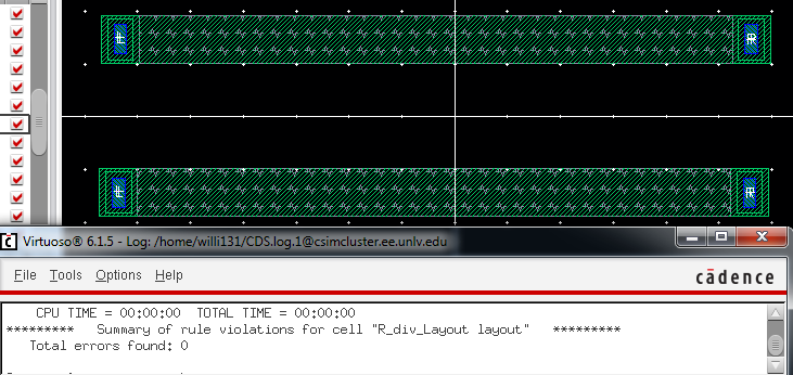
After
we added our resistors, DRC was run to ensure that spacing was within
acceptable limits. Shown above, there were zero errors found
meaning we are good to go!
Next we connected metal1 layers on the ends of each n-well resistor.
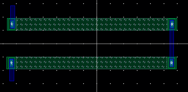
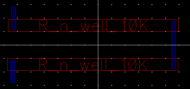
Just
to view our layout in different levels, above is shown with a scope of
10 layers. Below is shown with zero, meaning that you simply see
the basic picture.
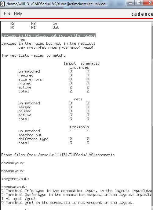
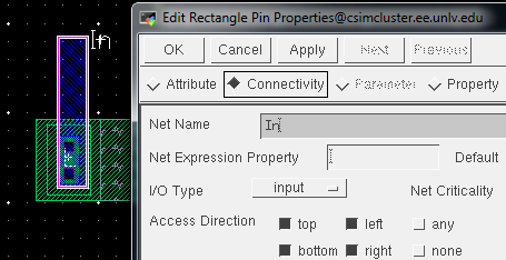
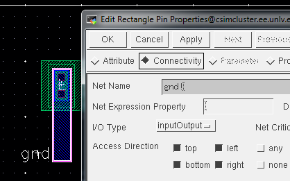
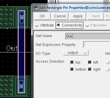
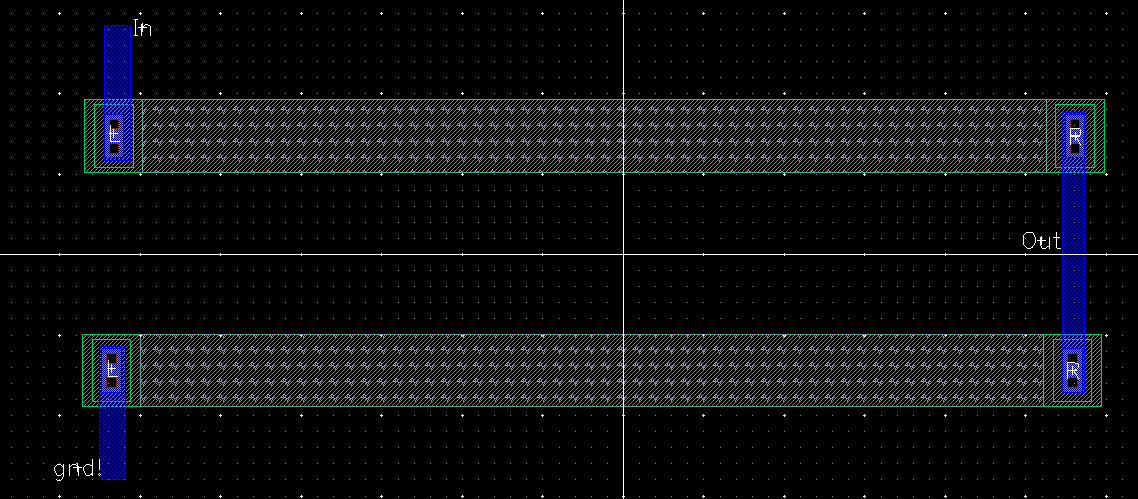
Next we connected pins In, Out, and ground to the n-well
resistors. DRC was ran to ensure no errors. Then the layout
was extracted. After success, LVS (Layout Vs Schematic check) was
run. Here I ran into an issue... As stated in the Tutorial, Pins
had to be reassigned properly as corresponding input/output/inputoutput
parameters with the schematic. Below shows these corrections.
The final Layout is shown below:
III. Backing up all Previous Lab and course work:
As shown below, all files from previous lab reports and course work were zipped and emailed to myself.
Post Lab 3:
This
lab focuses on the layout of the 10-bit DAC designed and simulated in
the previous Lab 2. Using the 10K n-well resistor created in
Tutorial 1.
I. Single Bit Layout using 10K n-well Resistors:
First,
using the 10K n-well resistors from Tutorial 1, I did a layout of a
single bit. You can see that there are two resistors in series
with a single resistor in parallel. The DRC came back with no
errors.
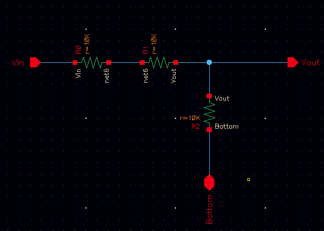
II.
Next, extracting the above layout I ran an LVS comparing my
layout to my original schematic of a single bit which is shown below.
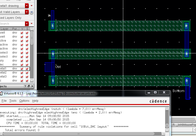
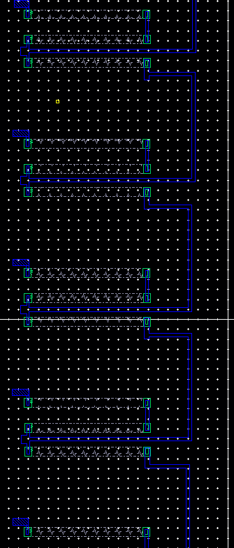
III. 10-Bit DAC Layout:
Next,
after a successful LVS I created a new layout. Here I
instanciated my single bit and then copied and pasted until my 10-bit
ladder was constructed. Using metal-1 constructed paths I
connected each bit as shown below. I then created pins for each
input B0-B9 as well as my final output pin. If you recall, in Lab 2
we implemented our original 10-bit DAC modelling a resistive ladder.
At the bottom of the B0 bit there were two 10K resistors in
series, rather than the single one at the bottom of the other bits in
the ladder. To mimic this design, I simply input another 10K
n-well resistor at the bottom of the ladder and then my gnd! pin
connected to the floating end of it. (You can see this in the
final Layout below.)
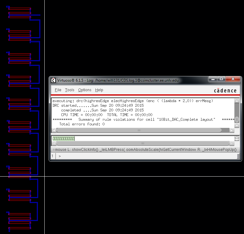
After completing my layout I ran a DRC successfully as shown above. Next, I extracted the layout as you can see below...
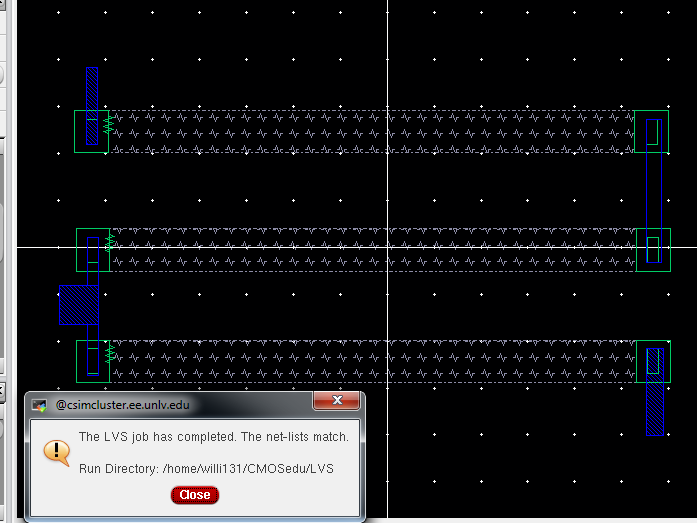
Finally, an LVS was ran to ensure that my Layout matched the 10-bit DAC schematic designed in my Lab 2.
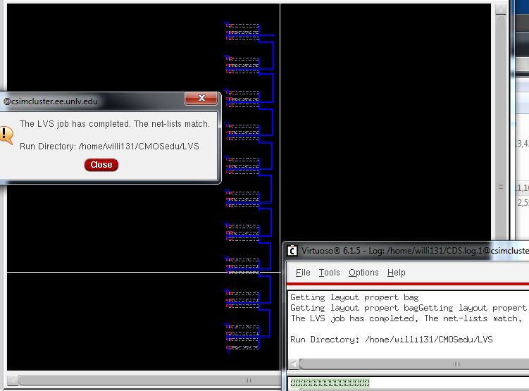
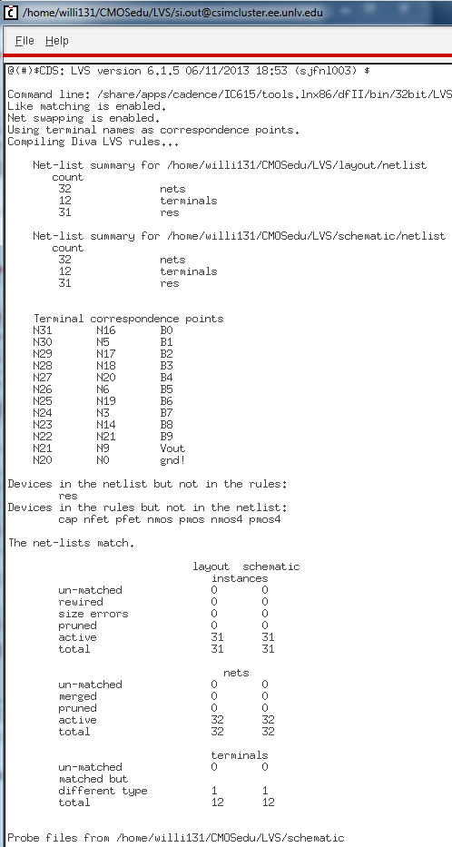
Above shows a successfully completed LVS of my 10-Bit DAC Layout.
IV. Back up
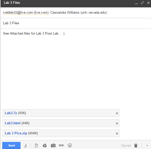
Here is a link to all my Cadence files for this lab.
Also, this file and all my work was emailed to myself and saved to my flashdrive as shown below.
Return to CMOSedu Courses Here.
Return to Student Lab Reports Here.