Lab 2 - ECE 421L 

Cassandra Williams

Willi131@unlv.nevada.edu

August 31, 2015


PreLab: 


The Prelab sets up directories for Lab2, running and simulating a 10-bit ADC-DAC circuit, and exploring what an ADC/DAC converter is and how it works.


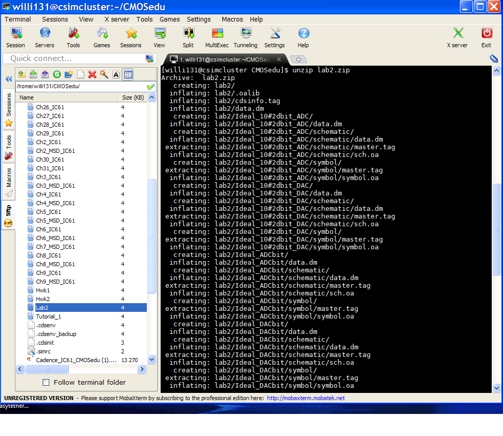
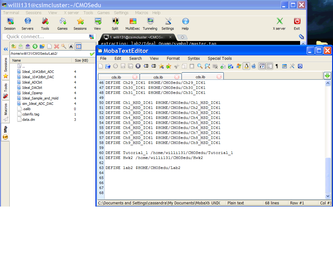
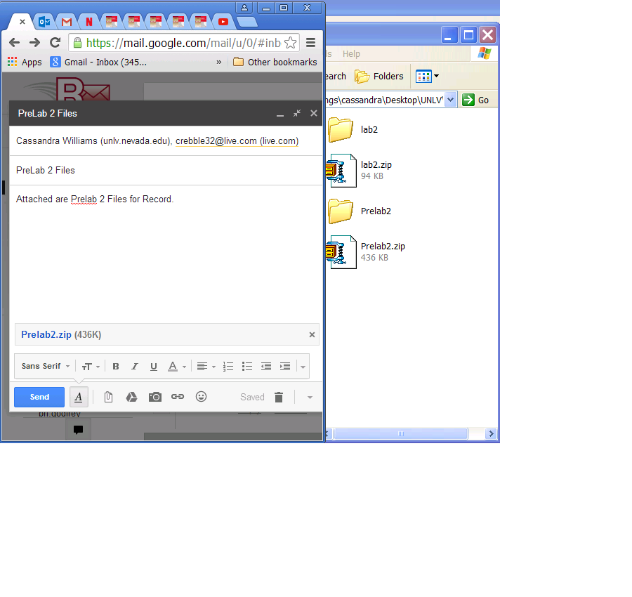
I.  First the lab2.zip was downloaded to my computer, then uploaded into my CMOSedu directory through MobaXterm.  Here I unzipped the file and adjusted my cdslib to accomodate the new directory Lab2.  Below are images showing these steps...


  http://cmosedu.com/jbaker/courses/ee421L/f15/students/willi131/Lab%202/PreLab%20Images/UnZip%20Lab2%20Image1.bmp


  http://cmosedu.com/jbaker/courses/ee421L/f15/students/willi131/Lab%202/PreLab%20Images/Lab2%20Directory%20and%20cdslib%20Image2.bmp


http://cmosedu.com/jbaker/courses/ee421L/f15/students/willi131/Lab%202/PreLab%20Images/Library%20Mgr%20ADC_DAC%20Image3.bmp


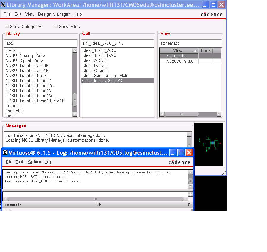
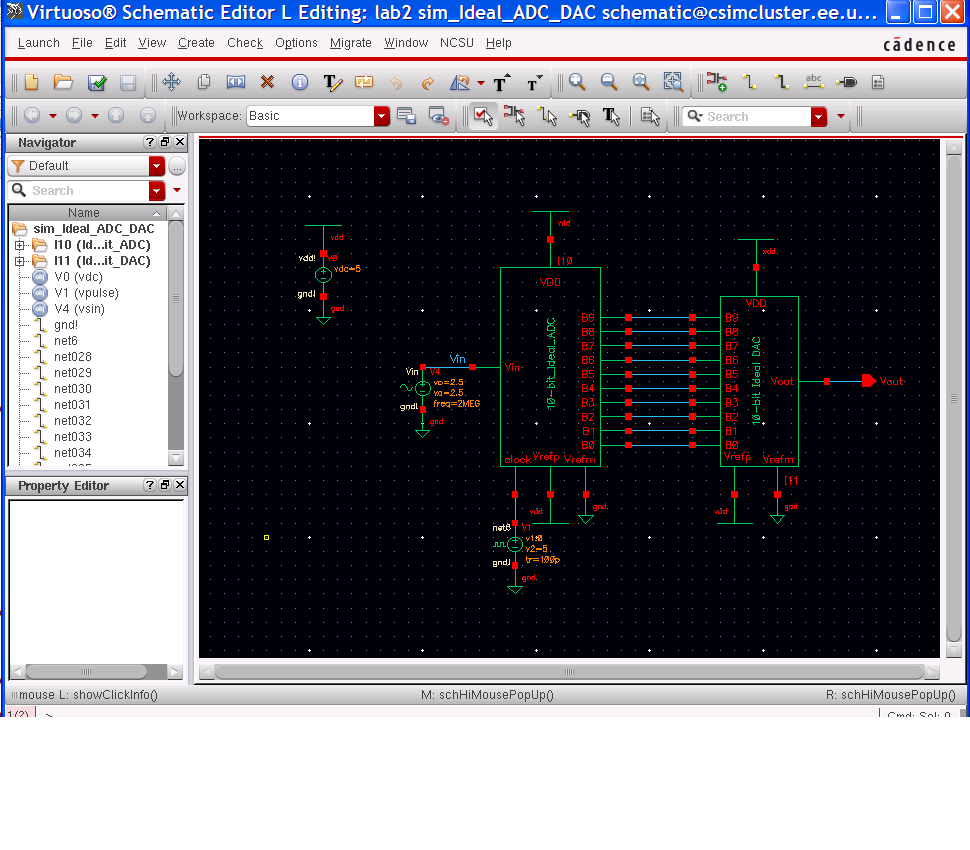
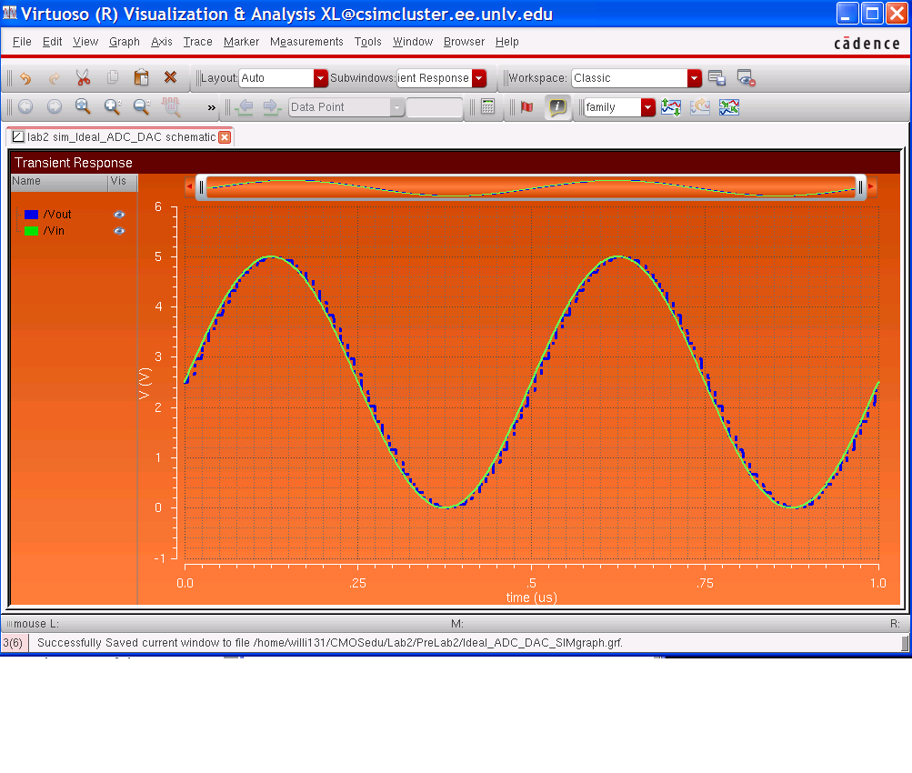
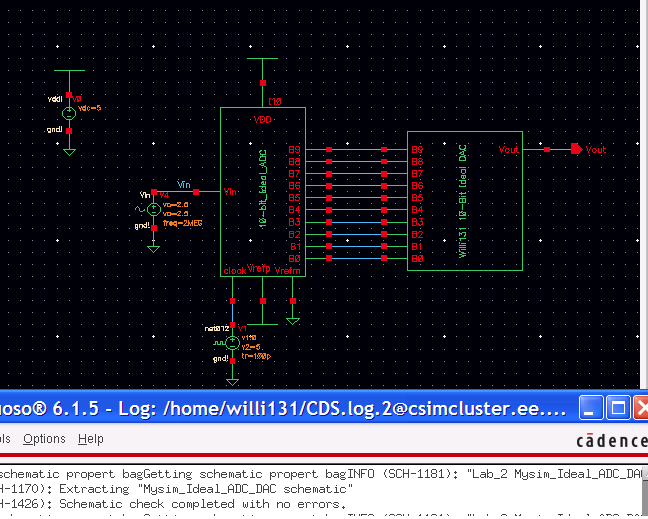
II.  Next, Cadence is started and sim_ideal_ADC_DAC is found under the Lab2 library.  The schematic is opened and simulated using the spectre_state1, which was created and preset previously...
   
   
 http://cmosedu.com/jbaker/courses/ee421L/f15/students/willi131/Lab%202/PreLab%20Images/Ideal%2010-bitADC_DAC%20Schematic%20Image4.bmp


Below is the simulation results showing Vin and Vout...
   
   
http://cmosedu.com/jbaker/courses/ee421L/f15/students/willi131/Lab%202/PreLab%20Images/Ideal%2010-bitADC_DAC%20Sim%20Graph%20Image%205.bmp


III. ADC-DAC explained:

     1.  Analog to Digital Converter

          a.  Analog input which is any signal that contains continuous values.

          b.  Digital output which is a discrete signal (made up of 1's and 0's).


Below shows a simple relationship between our (10-bit) Analog input (Vin) and corresponding Digital output B(0:9).  Also, the last column shows the decimal value which corresponds to the number of levels the output signal has.

                               INPUT                                         OUTPUT                      DECIMAL VALUE = LEVELS
                                   0 V          B0:                          0000 0000 00                                               0
                                     .
                                     .
                                     .
                                                 .
                                                 .
                                                 .
                                               .
                                               .
                                               .
                                  5V          B9:                          1111 1111 11                                   *2^10 = 1024


          c. Because in the lab we are using a 10-bit ADC we take 2 to the power of 10 in order to calculate the maximum levels of our output signal. Levels of our digital signal is called the                 resolution.


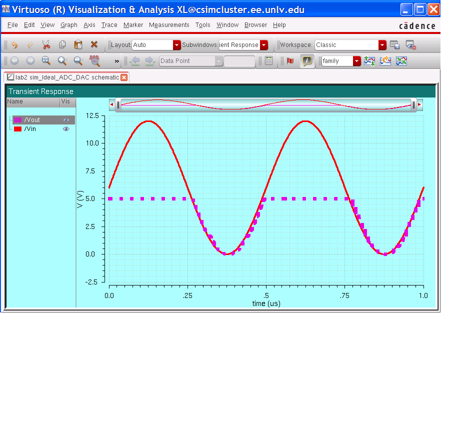
          d.  Below are a few examples of how varying the input can have an effect on the output.  Because the control voltage VDD is 5V, changing our input voltage from 2.5V as originally                    shown to 6V as shown below, we see that our output signal is capped at 5V.

           http://cmosedu.com/jbaker/courses/ee421L/f15/students/willi131/Lab%202/PreLab%20Images/5V%20Cap%20ADC_DAC%20Graph%20Image%206.bmp
 

     2. Digital to Analog Converter

         a. Digital input

         b. Analog output


As one would expect, a DAC works in the inverse way as the ADC taking a discrete digital signal and outputting a continuous analog signal. 

         c. various ways to accomplish this conversion

             1.  One method which we'll use in the lab is a resistive ladder.  This will be shown and explained in much further detail in the post lab.


III.  LSB- Least Significant Bit

      1. LSB is the minimum possible input voltage change required to have an effect and change our digital code output (B(0:9)).

          a. To calculate the LSB we use the following formula:


                                             Vin/(Output levels-1) = LSB value


          b. In our case of using the 10-bit ADC, with a voltage range of 0V to 5V, and 1024 levels (2^10) we have the following:


                                             5000 mV/ (1024-1) = 4.8876 mV 


              - This shows that any value below 4.8876 mV for an input will not have any effect on the output.


IV.  All work backed up by email and flash drive.
     
     http://cmosedu.com/jbaker/courses/ee421L/f15/students/willi131/Lab%202/PreLab%20Images/PreLab2%20Backup.bmp


_______________________________________________________________________________________________________________________________________________________
   
September 14, 2015
   
     
Post Lab Report:
   
 For our Lab 2 we designed a 10-Bit DAC using an n-well R of 10K.  (This is the Resistor Ladder mentioned in the prelab)

I.  Single Bit Schematic and Symbol
    a. First, creating a simple voltage divider as shown below my 2R resistor is made of two 10K resistors in series and then a single R being a 10K in parallel.  So this voltage divider is going to be a single bit.  You will see that in order to create a 10-Bit DAC, we will have to build it by using 10 of           these (Symbols created representing our voltage divider circuit) single bits.


                                                http://cmosedu.com/jbaker/courses/ee421L/f15/students/willi131/Lab%202/Lab2%20Images/1.%20DAC%20Bit%20Symbol%20Schematic%20.PNG
   
   
       b.  After I checked and saved the above schematic with a "no error" result I created my single-bit symbol to be used as my building blocks for my 10-bit DAC.
 
 
                                                http://cmosedu.com/jbaker/courses/ee421L/f15/students/willi131/Lab%202/Lab2%20Images/2.%20DAC%20Bit%20Symbol.PNG


c.   Next I used the above block to create my 10-Bit DAC schematic shown below.
 
 
                                  http://cmosedu.com/jbaker/courses/ee421L/f15/students/willi131/Lab%202/Lab2%20Images/3.%20DAC%2010-Bit%20Symbol%20Schematic.PNG


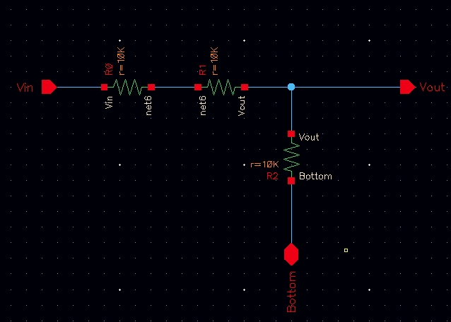
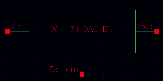
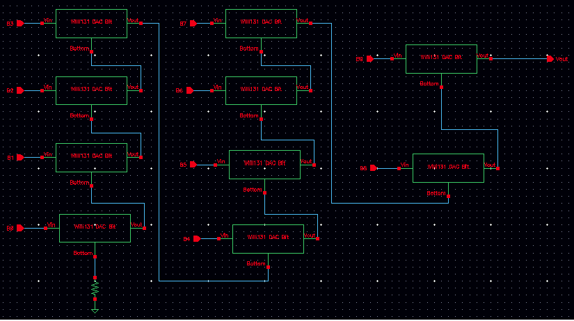
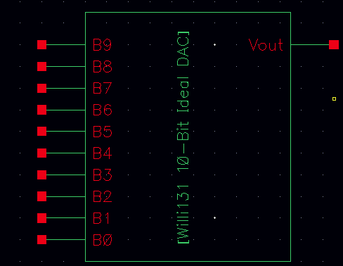
              d. The above schematic follows the original example of the resistor ladder.  We have B0-B9 inputs and a single Vout output.  Below is the DAC symbol created:


                                                                           http://cmosedu.com/jbaker/courses/ee421L/f15/students/willi131/Lab%202/Lab2%20Images/4.%20My%20Design%20DAC%2010-Bit%20Symbol.PNG


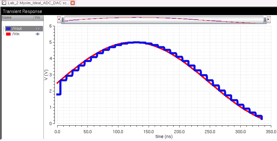
          f. So at this point I wanted to make sure my symbol is just like the ideal DAC used in the original ADC-DAC schematic from the prelab.  So I copied the original schematic and replaced the DAC in it with my own designed one.  As you can see, the results are the same showingthat the DAC I created is comparable to the original. :)


                                                              http://cmosedu.com/jbaker/courses/ee421L/f15/students/willi131/Lab%202/Lab2%20Images/5.%20MyDesign%20Test%20Sim%20Schematic.PNG


                                                                                                                                                                                                                                                                                                                http://cmosedu.com/jbaker/courses/ee421L/f15/students/willi131/Lab%202/Lab2%20Images/6.%20MyDesign%20Test%20Graph.PNG


 II.  Delay and Driving a Load


        a. 10pF Cap Load:

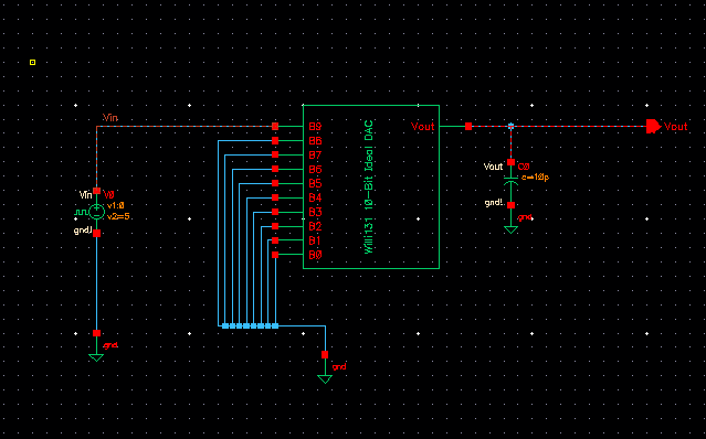
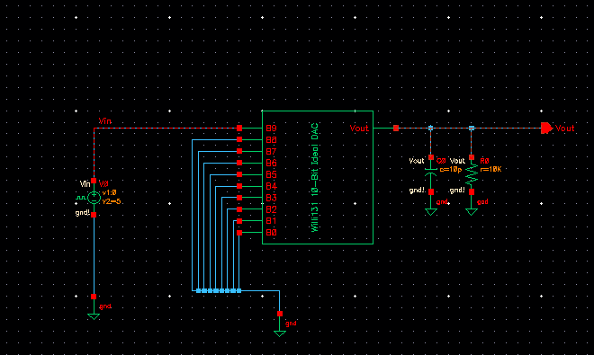
            First we were to ground all pins except B9 which was connected to a PULSE Voltage source going from 0V to 5V, and connect a 10pF Capacitor to the output of our DAC.. According to my calculations using the equation for delay of td = .7RC , the delay of our circuit should be about 70ns.   Below is the circuit constructed and the simulation output.


                                                   http://cmosedu.com/jbaker/courses/ee421L/f15/students/willi131/Lab%202/Lab2%20Images/7.%20Cap%20Schematic.PNG


                                   http://cmosedu.com/jbaker/courses/ee421L/f15/students/willi131/Lab%202/Lab2%20Images/8.%20Cap%20Graph.PNG

****(So due to not so steady hands, the marker shows a 72.5ns delay, however it is not exactly in the right spot showing the accurate 70ns, but its close)


           b. Driving 10pF Cap AND 10K Load:

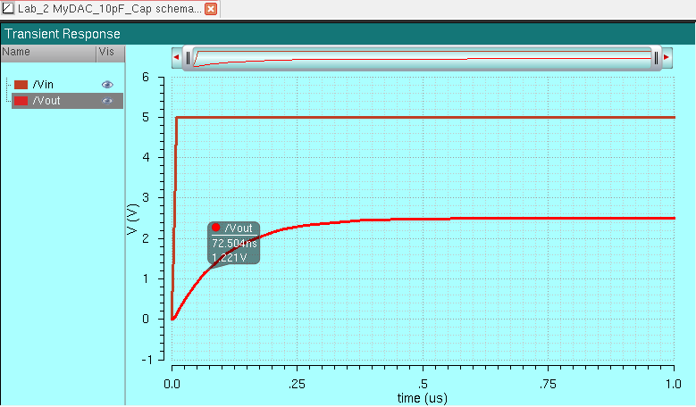
                Next, modifying the schematic, in addition to the 10pF capacitor a single 10K Resistor was added in parallel.  This demands the circuit act similar to a voltage divider causing our output to just about drop to half of the first simulation with solely a capacitive load. (Still using the same delay equation, (.7*10p*5K)  *** 5K is the result of our load 10K  resistor and our DAC (10K n-well resistor) in parallel with each other**


                                                      http://cmosedu.com/jbaker/courses/ee421L/f15/students/willi131/Lab%202/Lab2%20Images/9.%20Cap%20and%20Res%20Schematic.PNG


                                                       Below you can see that the output voltage has dropped and the delay was shortened as well.


                                        http://cmosedu.com/jbaker/courses/ee421L/f15/students/willi131/Lab%202/Lab2%20Images/10.%20Cap%20and%20Res%20Graph.PNG


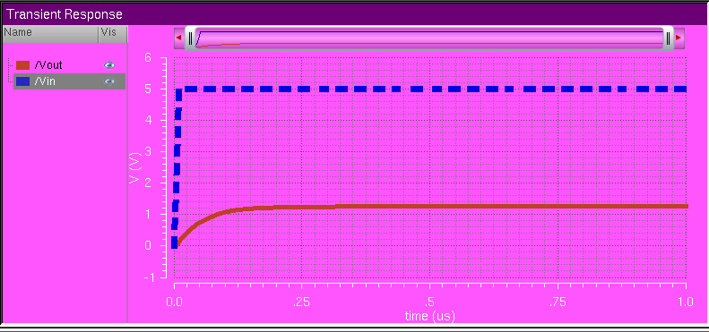
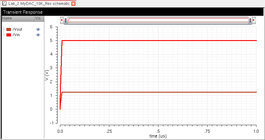
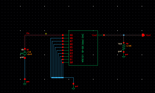
           c.  Driving a 10K Resistive Load:

                Finally, I modified the circuit one more time by removing the capacitor.  Now we have a very simple voltage divider.  This should merely cut the voltage value in half.


                                      http://cmosedu.com/jbaker/courses/ee421L/f15/students/willi131/Lab%202/Lab2%20Images/11.%20Res%20Schematic.PNG


                            And below is my resulted simulation showing my predictions were mostly correct.  The output voltage is indeed much less that the input voltage.  This result, not being exactly half of the input voltage as expected could very possibly be due to parameters/errors within my design.


                          http://cmosedu.com/jbaker/courses/ee421L/f15/students/willi131/Lab%202/Lab2%20Images/12.%20Res%20Graph.PNG


               d.  So in a real circuit the switches shown the the resistor ladder circuit from the prelab (ADC outputs) would be implemented with transistors.  If the resistance of the switches isn't small compared to R, the output voltage would decrease even more.  This would be caused by a parasitic resistance of the transistors being equivalent to 2R.  Adding this to our circuit would cause a series resistance of 4R being paralleled with a single R resistance.   This intuitively in turn will cause the decrease in our output voltage.


III.  Back-up  


                                                               http://cmosedu.com/jbaker/courses/ee421L/f15/students/willi131/Lab%202/Lab2%20Images/Back%20up%20Proof.PNG   


           Files and images were zipped into the Lab2 file originally saved from the prelab and emailed to myself.  Also these are saved on a flashdrive.


 Return to EE 421 L


Return to Student Labs