1. Create a pad 75 um.
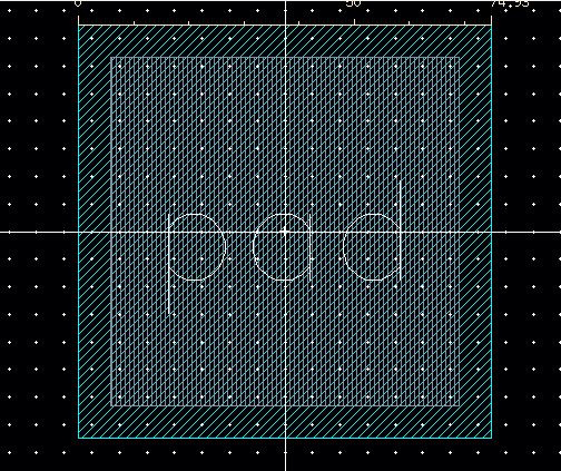
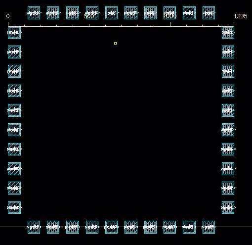
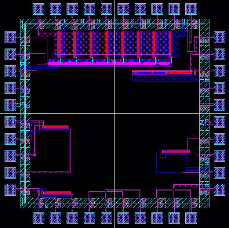
2. Once the pad is created we can use it to layout padframe about 1.5mmX1.5mm.
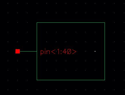
Symbol
Layout
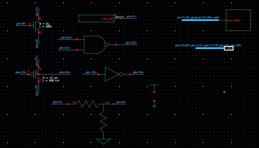
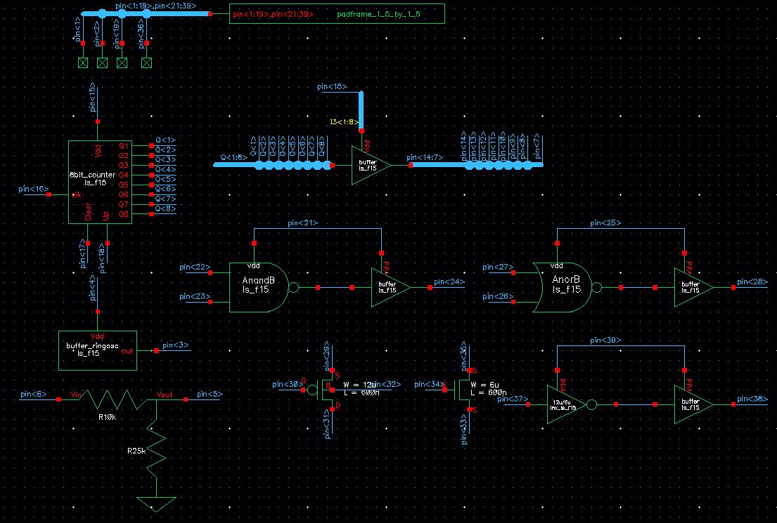
3. Now we start with an schematic of all the components in the chip and assign the pins.
Lab 8 - EE 421L Fall 2015
Chip 7
Co Nguyen
nguyec3@unlv.nevada.edu
Zip folder containing Chip7 files found here.
Note: Inside the chip file there is a more detailed instructions on how to test the chip, and the required connections.
Pre-lab
work
Form
into groups of 4 students that will put the test structures on the chip.
Each test circuit should have its own power but ground should be
shared
between the circuits.
Power should not be shared between the circuits so that
a vdd!-gnd!
short in one circuit doesn't make one of the other
circuits inoperable.
Your chip should include the following test structures:
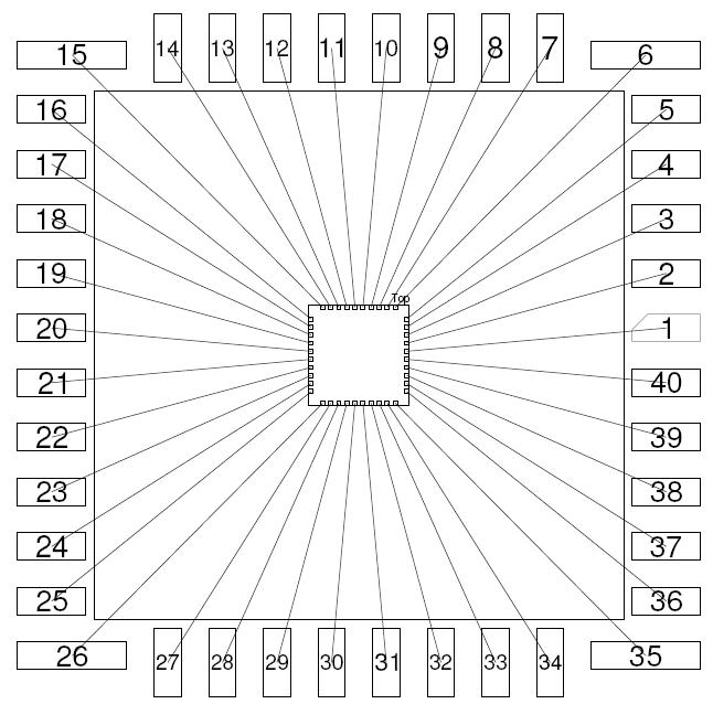
| Pin Number | Description | Notes |
| 1 | Not used | |
| 2 | Not used | |
| 3 | vdd(31-stage Ring Oscillator) | +5 V |
| 4 | Oscillator_Out(31-stage Ring Oscillator) | |
| 5 | Vout (Voltage divider) | To meausere the 10k resistor use pin 5 and pin 6 with no vdd applied |
| 6 | Vin (Voltage divider) | To measuere the 25k resistor use pin 5 and pin 20. |
| 7 | Q8(8 bit up/down counter) | MSB |
| 8 | Q7(8 bit up/down counter) | |
| 9 | Q6(8 bit up/down counter) | |
| 10 | Q5(8 bit up/down counter) | |
| 11 | Q4(8 bit up/down counter) | |
| 12 | Q3(8 bit up/down counter) | |
| 13 | Q2(8 bit up/down counter) | |
| 14 | Q1(8 bit up/down counter) | LSB |
| 15 | vdd (8 bit up/down counter) | +5 V |
| 16 | Clock in (8 bit up/down counter) | |
| 17 | Clear (8 bit up/down counter) | Clear=1 will clear the counter |
| 18 | Up/Down (8 bit up/down counter) | 1= Up count, 0=Down count |
| 19 | Not used | |
| 20 | GROUND | This pin is used as ground for all the circuits |
| 21 | vdd (NAND GATE) | +5 V |
| 22 | A input (NAND GATE) | |
| 23 | B input (NAND GATE) | |
| 24 | Output (NAND GATE) | |
| 25 | vdd (NOR GATE) | +5 V |
| 26 | B input (NOR GATE) | |
| 27 | A input (NOR GATE) | |
| 28 | Output (NOR GATE) | |
| 29 | Source (PMOS) | |
| 30 | Gate (PMOS) | |
| 31 | Drain (PMOS) | |
| 32 | Body (PMOS) | |
| 33 | Source (NMOS) | |
| 34 | Gate (NMOS) | |
| 35 | Drain (NMOS) | Note the body of the NMOS is grounded |
| 36 | Not used | |
| 37 | Input (inverter) | |
| 38 | Output (inverter) | |
| 39 | vdd (inverter) | +5 V |
| 40 | VDD | +5 V |
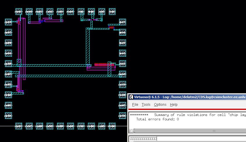
Full layout of the MOSIS chip
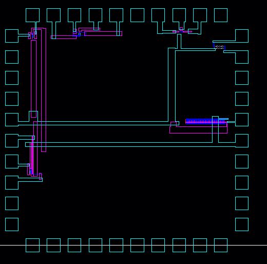
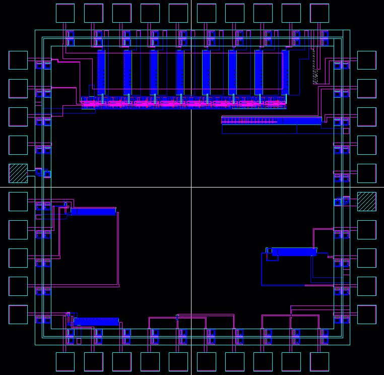
Full extract of the MOSIS chip
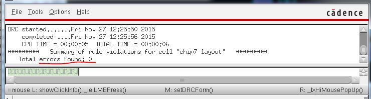
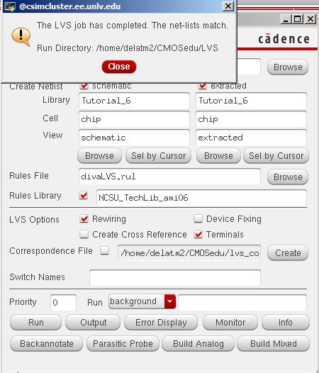
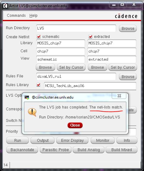
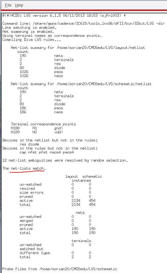
LVS-no error- of MOSIS Chip
Return to EE421L - Student Lab Reports