Lab 4 - ECE 421L
Authored
by: Cesar Nieves
Today's
date: September 15, 2021
Email: nievec2@unlv.nevada.edu
Lab
description:
- In this lab we will be continuing what we did in the previous lab, layout schematic.
- We will also be simulating schematic of Nmos and Pmos transistors.
Pre-lab:
- First, we had to read through the lab 4 page, which tells us what we are going to be doing.
- Lastly, was just go through the Turtorial 2 page to set up what we will be using in class (below are some of what was asked for).
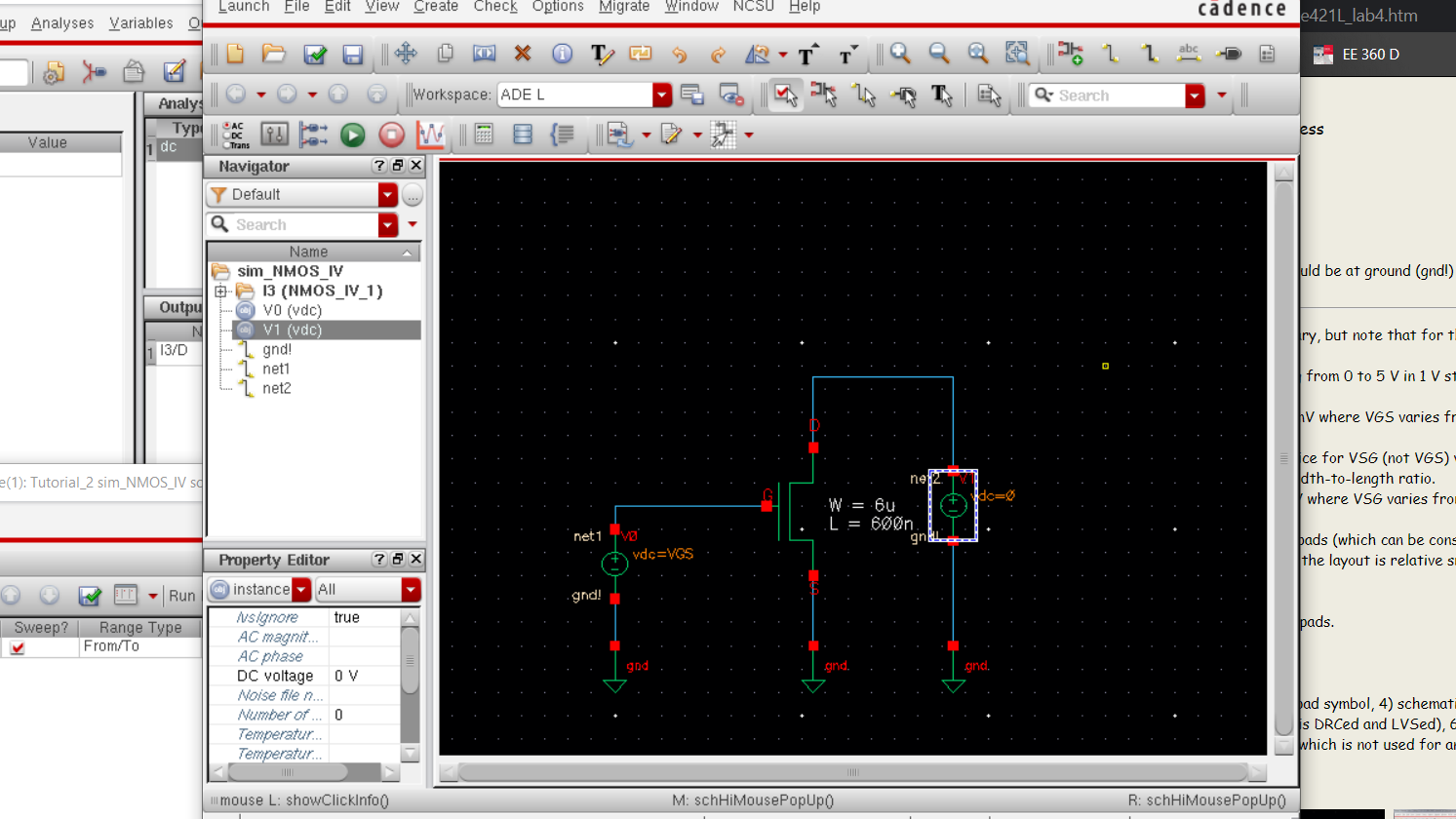
NMOS
This is then turn into a symbol and then into layout.
After the layout we extract it.
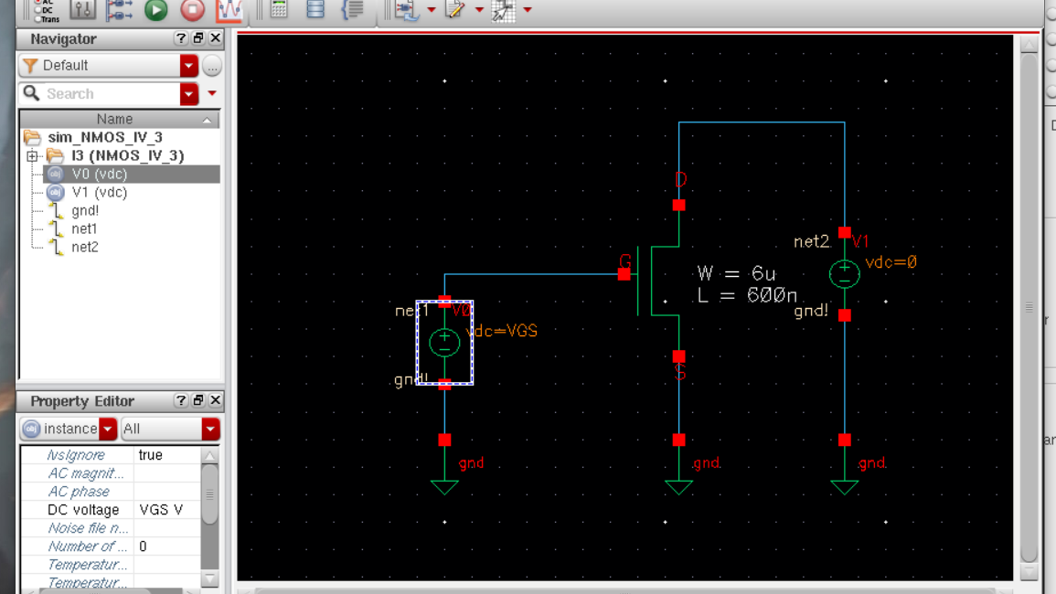
During the analysis process, we find out that we need to make the NMOS into a 4 terminal and fix the previous work
. 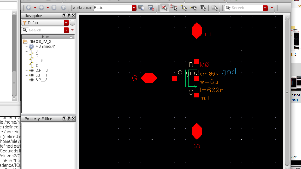
Then, we added it to a circuit so we can see the results.
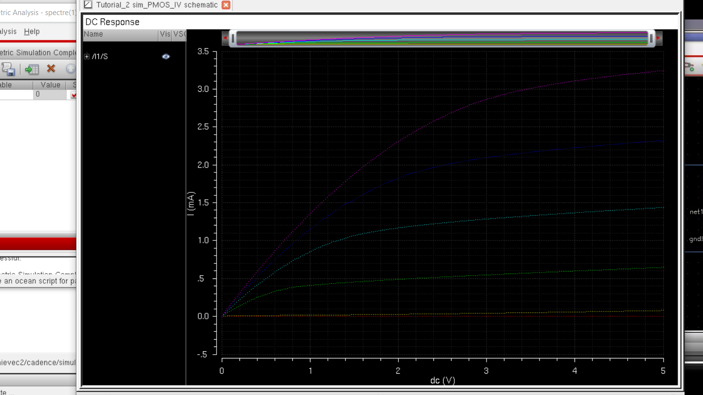
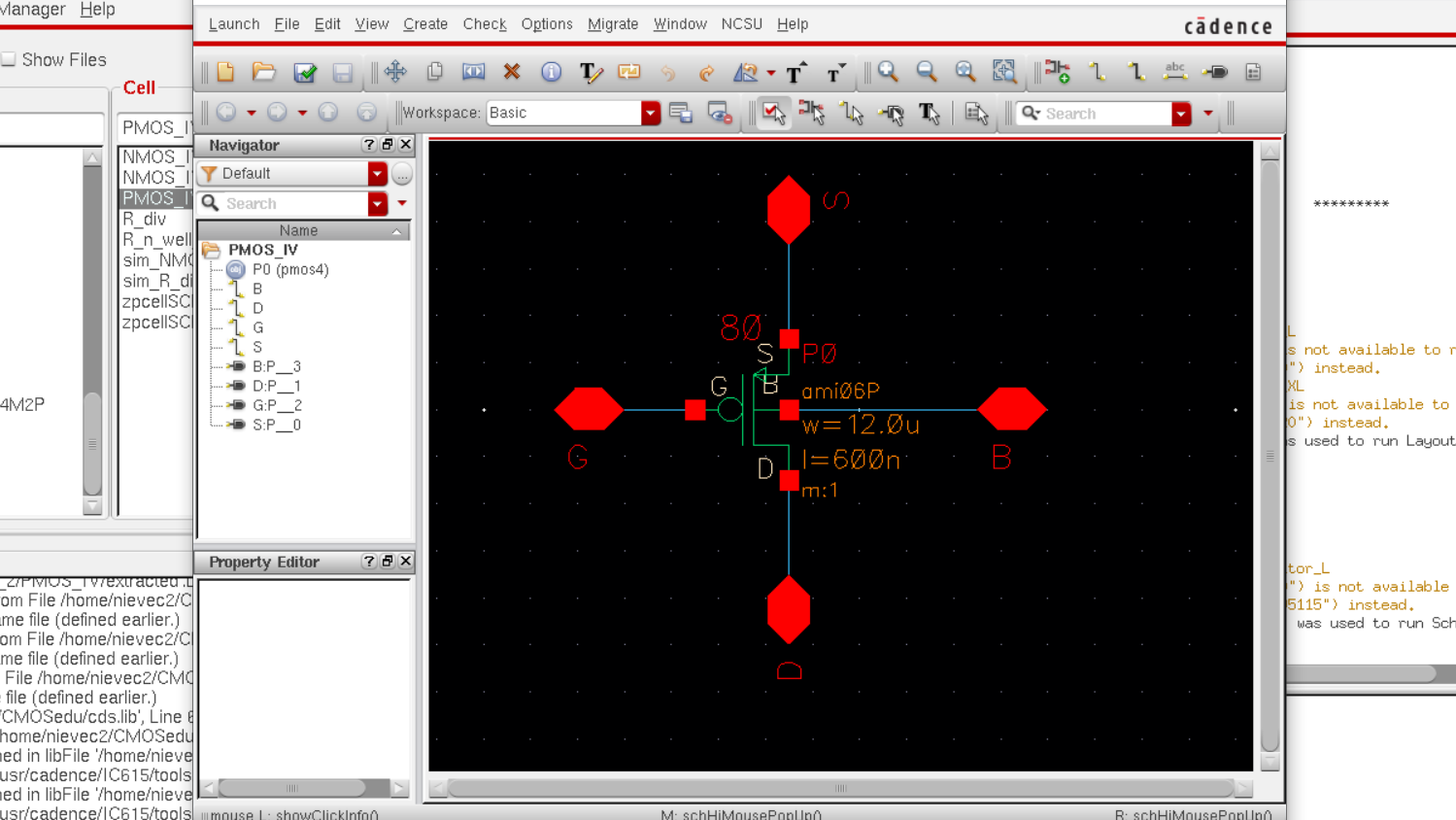
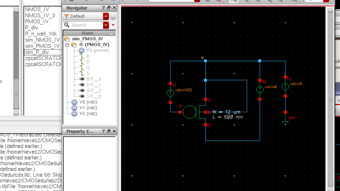
PMOS Version with my data
Lab:
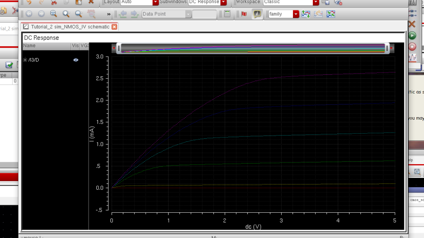
A schematic for simulating ID
v. VDS of an NMOS device for VGS varying from 0 to 5 V in 1 V steps
while VDS varies from 0 to 5 V in 1 mV steps. Use a 6u/600n
width-to-length ratio.
A
schematic for simulating ID v. VGS of an NMOS device for VDS = 100 mV
where VGS varies from 0 to 2 V in 1 mV steps. Again use a 6u/600n
width-to-length ratio.
(Cadence was not letting me change the value for VDS to 100 mv)
A
schematic for simulating ID v. VSD (note VSD not VDS) of a PMOS device
for VSG (not VGS) varying from 0 to 5 V in 1 V steps while VSD varies
from 0 to 5 V in 1 mV steps. Use a 12u/600n width-to-length ratio.

A
schematic for simulating ID v. VSG of a PMOS device for VSD = 100 mV
where VSG varies from 0 to 2 V in 1 mV steps. Again, use a 12u/600n
width-to-length ratio.
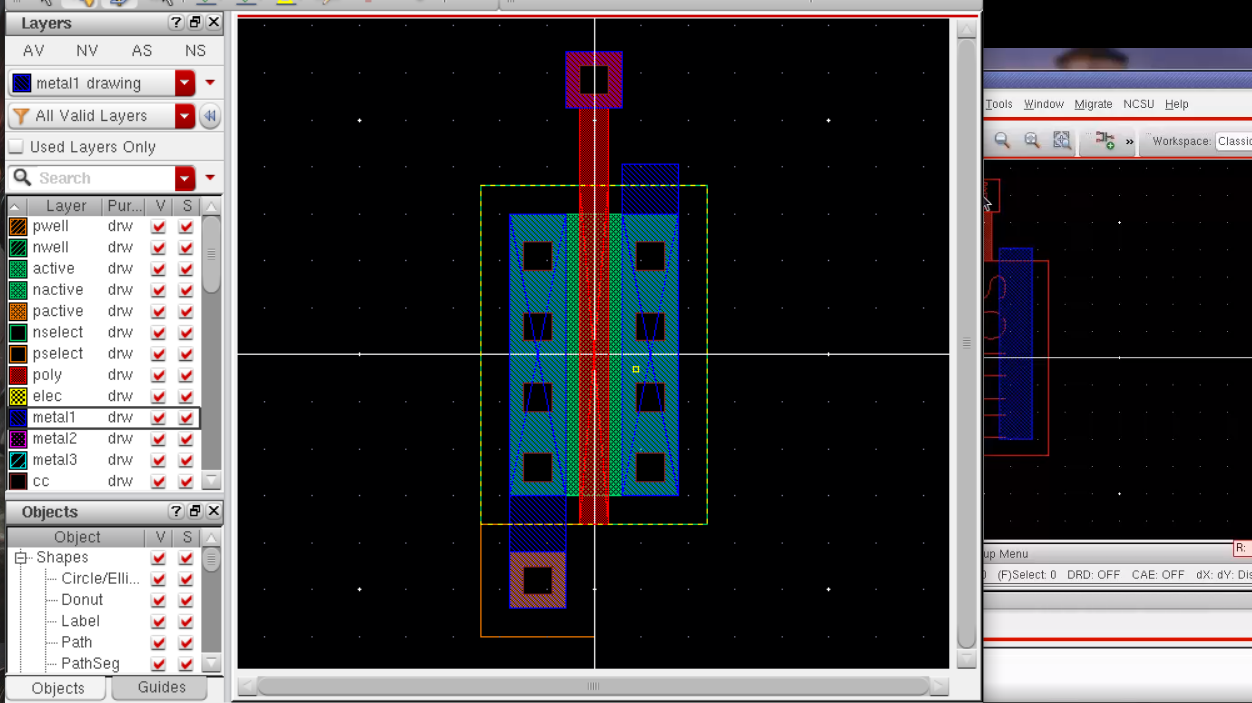
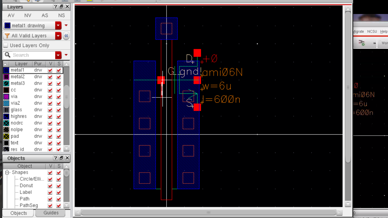
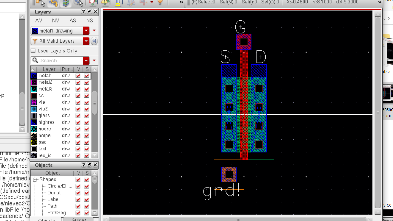
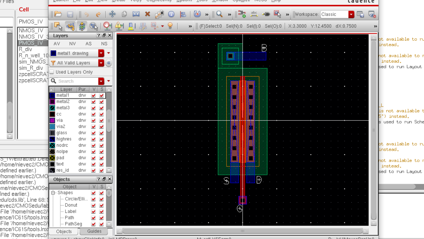
Lay
out a 6u/0.6u NMOS device and connect all 4 MOSFET terminals to probe
pads (which can be considerably smaller than bond pads [see MOSIS design rules] and directly adjacent to the MOSFET so the layout is relative small).
Lay out a 12u/0.6u PMOS device and connect all 4 MOSFET terminals to probe pads.
This is the end of the fourth lab.
Return