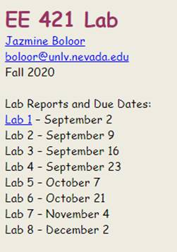
Lab 1 - EE 421L
Email:
boloor@unlv.nevada.edu
Lab description: Laboratory
introduction, generating/posting html lab reports, installing and using Cadence.
Pre-Lab Work
The lab reports will be drafted using html and placed on CMOSedu.
Prior to the first day of lab, but no earlier than one week before
the lab starts, get a CMOSedu account, using your
UNLV email address, from Dr. Baker, rjacobbaker@gmail.com
Review the material seen here covering editing webpages (do this before the first
lab)
For the prelab, my CMOSedu account was
made and I reviewed the editing webpages material from CMOSedu.com.
The following snips show the index and the URL of my CMOSedu page:
![]()
Lab Work
The first part of lab 1 goes through the first 25 steps of the first tutorial on
CMOSedu.com.
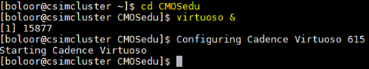
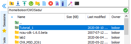
To launch Cadance and use the CMOSedu directories, I logged into MobaXterm
using the “cd” and “virtuoso &” commands shown in yellow in the following
snip.
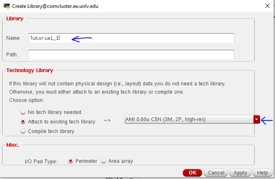
Next, I created a library (File > New > Library) and changed
the title to Tutorial_1. I attached the AMI 0.60u C5N (3M, 2P, high-res)
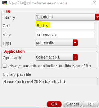
library using the scroll bar. Once this library was created, I added a cell
called “R_div” by clicking File > New > Cell
View and inputting the title of the Cell. The other selections in this window
(shown to the right) were left the unchanged.
Creating a new library Creating a new cell
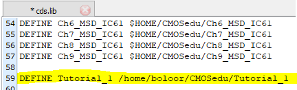
I added the following DEFINE statement to my cds.lib because a new
library was added in the previous step.
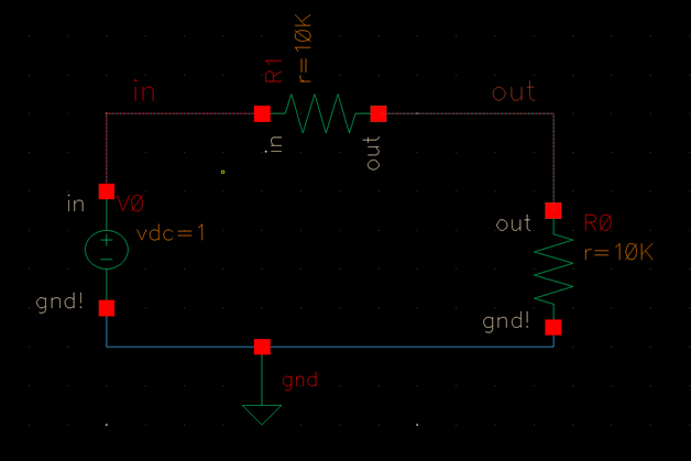
The tutorial this lab follows calls for the design of a voltage divider.
To draft the components necessary for this, I clicked Create > Instance
(bind key I) and found the components necessary. I also labeled the
wires using the Create Wire Name function in the toolbar. The following snips show the final schematic
and transient waveform for the voltage divider built.
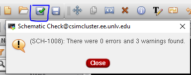
I used the Save and Check function and no errors were found.
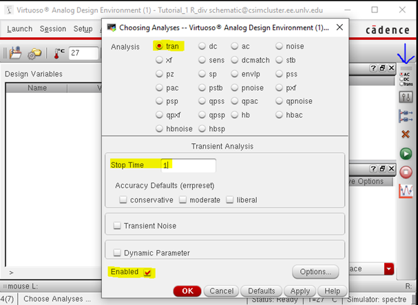
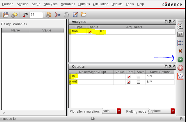
I set my simulator to Spectre (Setup
> Simulator/Directory/Host), and then clicked on “Choose Analysis” shown
below with an arrow, and then entered the information highlighted.
Next, I clicked Outputs > To Be Plotted > Select on
Schematic and selected the wires shown my above schematic named “in” and “out”.
The simulation was ready to be run by pressing the green “Netlist and Run”
button shown with an arrow below.
The following analysis was formed. I changed the line widths to medium,
style to solid, and used more contrasting colors by right clicking on the
signal name and editing the properties.
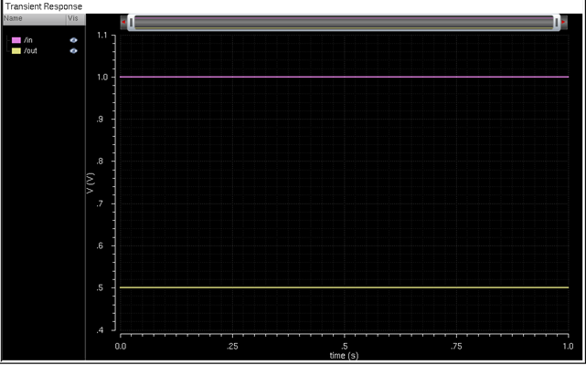
The output of a voltage divider is expected to be half of its
input. The input here shows 1V (directly pulling from the voltage source), and
the output shows 0.5V. Therefore, the simulation is exactly what we expected.
The second part of lab one was to
stress the importance of backing up work and show how to do it.
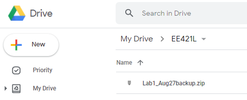
To illustrate this, I will show how I
backed up Lab 1 by saving a copy to my Google Drive.
First, I downloaded a copy of the Tutorial_1 file to my Desktop
and zipped the contents.

Then, I created a new folder in my Google Drive called “EE421
Lab”. Once this folder is open, the zipped-up Tutorial_1 folder can be dragged
and dropped in. I renamed the file Lab1_Aug27backup to stay consistent with the
other labs I will put in this folder.
That concludes the lab work.