Lab 2 – Design of a 10-bit Digital-to-Analog Converter (DAC)
EE 421L Digital IC Design
Lab Date: 9/04/19 Due: 9/11/19
Last Edited on
9/04/19 at 8:13am using Word
In this lab,
we will be first unzipping a premade ideal 10-bit Analog-to-Digital Converter
(ADC) and 10-bit DAC Converter into our Cadence design directory on MobaXterm.
First download
the lab2.zip file provided from the pre-lab.
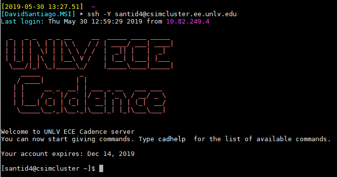
Now, log on to
the csimcluster SSH using MobaXterm
(or whatever you use).
Assuming you
have installed (and followed Dr. Baker’s Intro to
Installing Cadence Tutorial), go to your CMOSedu
directory by typing:
-
cd CMOSedu
And also go to that directory using the Sffp tab to your
very left of the screen.
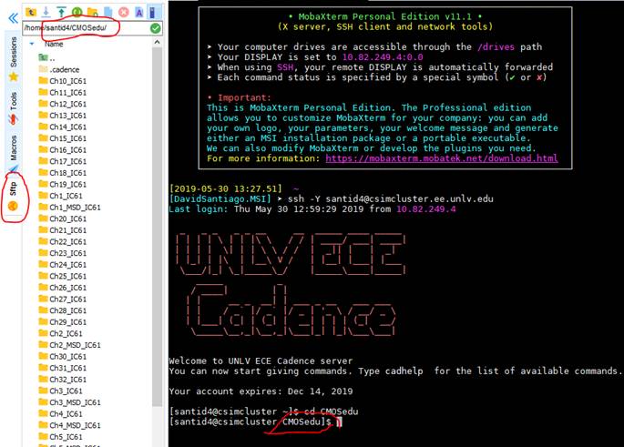
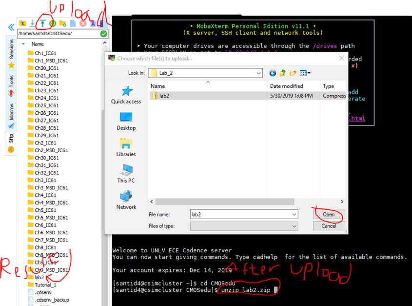
In this
directory, we will upload the lab2.zip file (from wherever you downloaded it),
and then extract it using the following command:
-
unzip lab2.zip
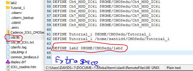
After that,
locate the cds.lib file in the CMOSedu directory, right click and open
up the default text editor. Once open, type onto the bottom of the file
(and entering a few newlines after the text):
-
DEFINE lab2
$HOME/CMOSedu/lab2
And this will
setup the library in Cadence.
Save, click
yes to whatever box pops up (that’s if something does appear), and close the
text file.
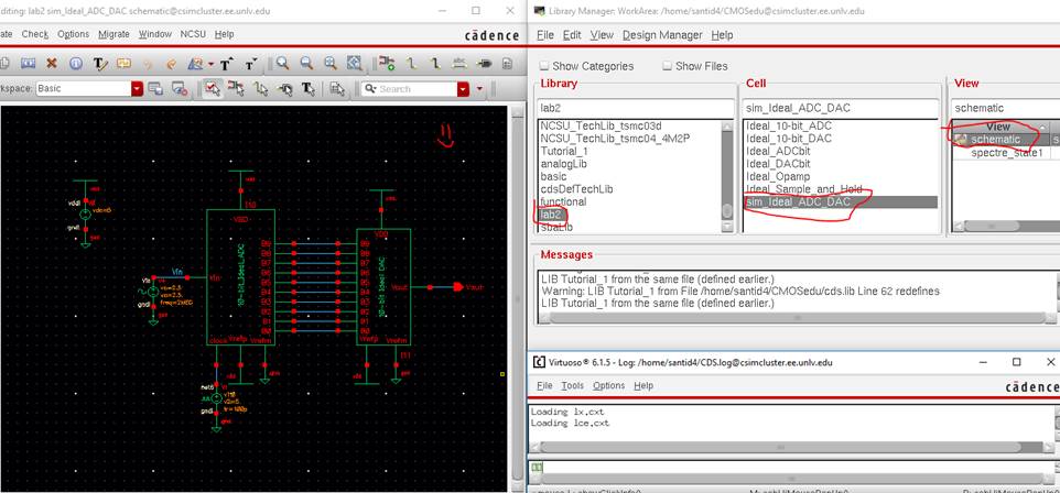
We will now
start Cadence’s Virtuoso program in the CMOSedu
directory using:
-
virtuoso &
and navigate
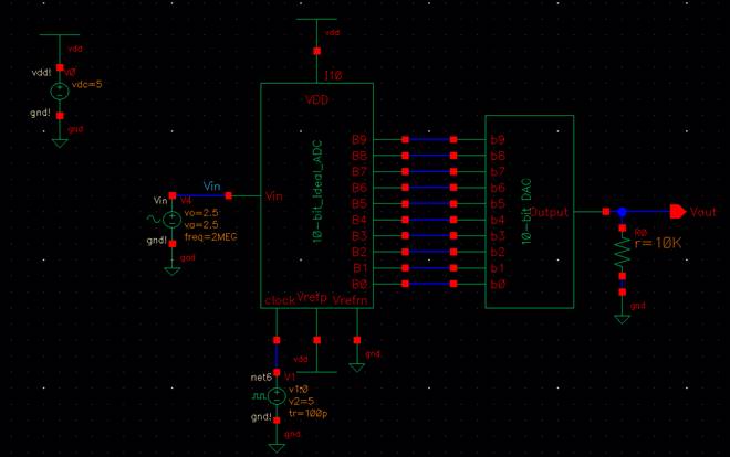
to the lab2 library, and open up the sim_Ideal_ADC_DAC schematic under the Cell menu.
- If no
library shows (just the Cadence command window), click on Tools -> Library
Manager
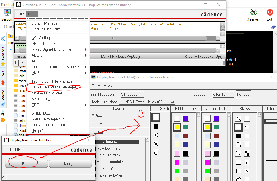
Suppose you want
to change the color of the schematic or change the size of the lines of the
traces. We can do that by clicking (in Cadence’s Command Interpreter Window)
Tools -> Display Resource Manager. Click on “Edit” and you’ll see a nice
colorful window appear.
On the Display
Resource Editor, click on the “All” Layers tab.
Now on the
bottom, you’ll see a lot of stuff, scroll down till we see the “Wire Drawing”
layer.
The Default is
Cadet Blue, and we will
change it to Blue.
Change the
Fill and Outline color to the new color, and while we are here, change the line
style to a thicker line.
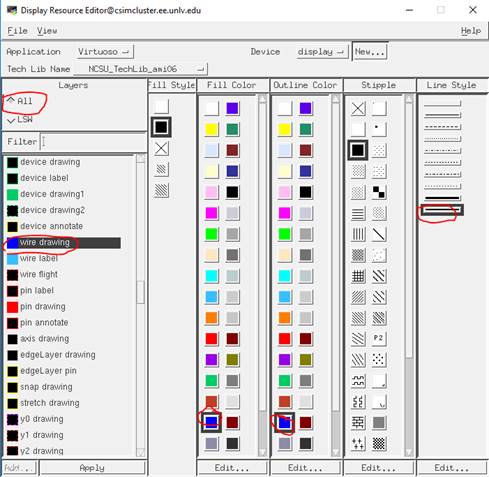
Click “Apply” at
the bottom of the window, and then File -> Save
On the new
window, click on the display.drf
file, and then OK
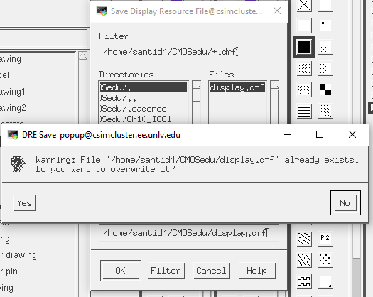
Overwrite the
file, and click “Yes”
If you had a
schematic open, close it and reopen it, and the new changes will appear.
Repeat till
you are satisfied with your new colorful circuit (ᵔᴥᵔ)
Lets run a simulation of the above circuit.
On the
schematic window, click Launch -> ADE L,
In the Analog
Design Environment window, click Session -> Load State
In this newer
window, click on Cellview, and then press OK.
In the Analog
Design Environment Window, press the Green Start Button and the following will
appear:
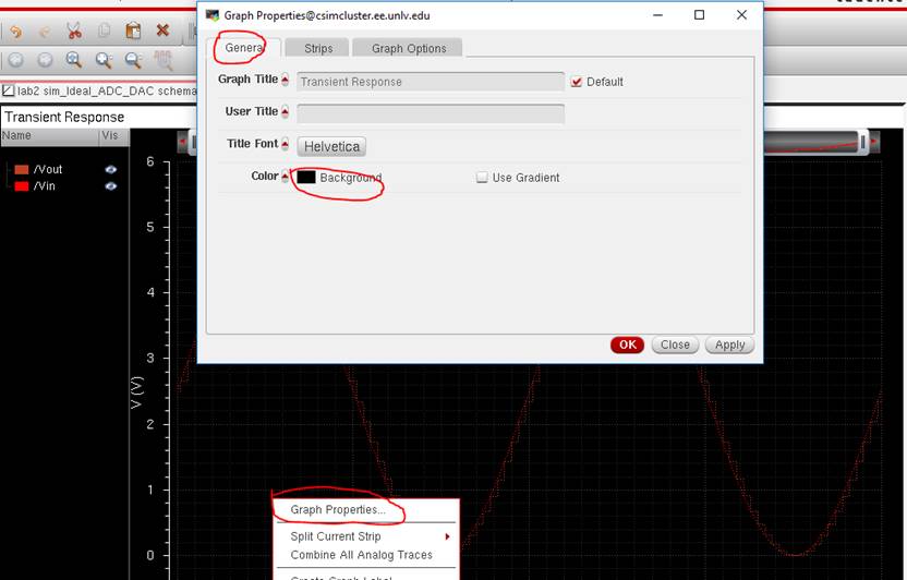
To change the
background of the Simulator, right click on the plot, Click on Graph
Properties.
Then hit the
General Tab, and change the color of the background to
whatever color you desire.
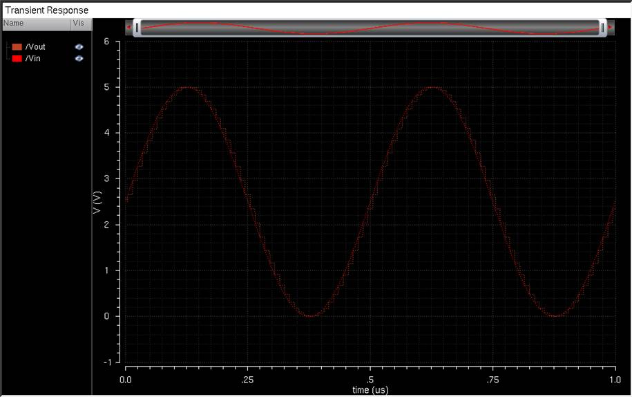
After changing
the background (and returning to how to change colors of stuff using the
Display resource manager), this is the result:
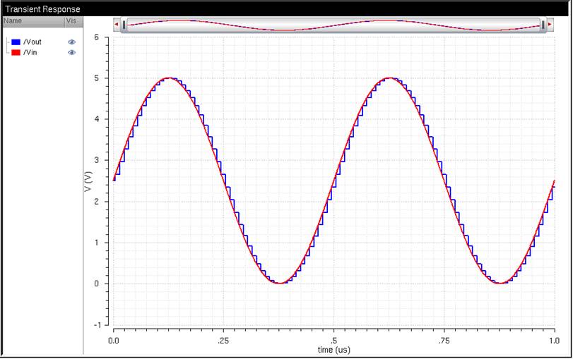
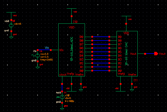
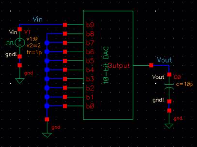
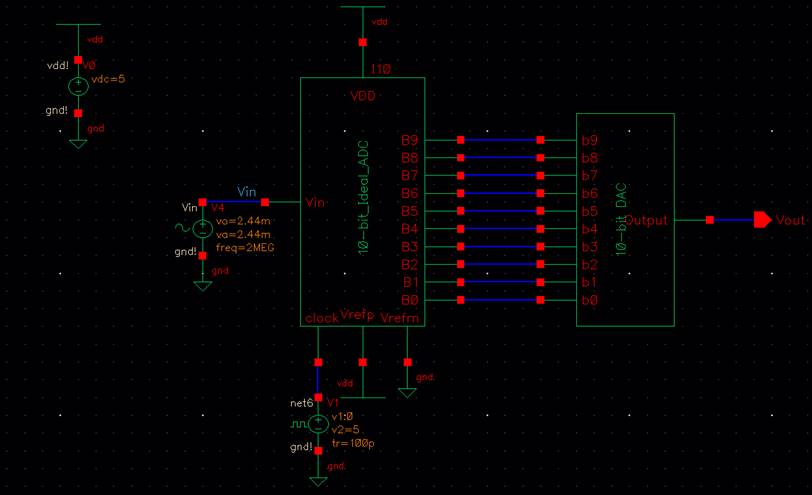
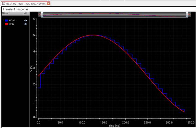
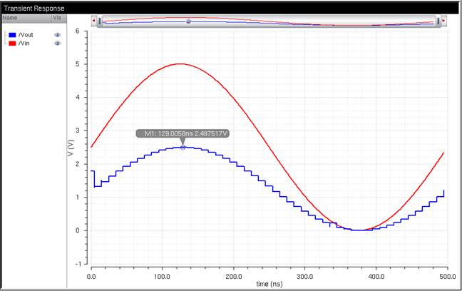
Vin (Red) is a sine
wave being fed into an ADC converter, with the output being a 10-bit value. Vout (Blue) is the output of the 10-bit values
going through into the DAC converter.
For the ADC,
we will have a step size, which is calculated by:
-
Step Size = VCC / 2N ,
with N = 10 bits
Vin is then
converted into a digital number:
-
Digital Value = Vin / Step Size, where if Vin = VCC,
the Digital value = 2N.
For this Lab,
VCC = 5V,
So the Step Size is = 5V / 210 = 4.88mV.
This means for
1 bit, we need around 5mV each bit.
Lets prove it by changing the input AC signal to an amplitude of 5mV.
We do that by
clicking on Vin, and pressing bindkey
q (or clicking Edit -> Properties -> Objects).
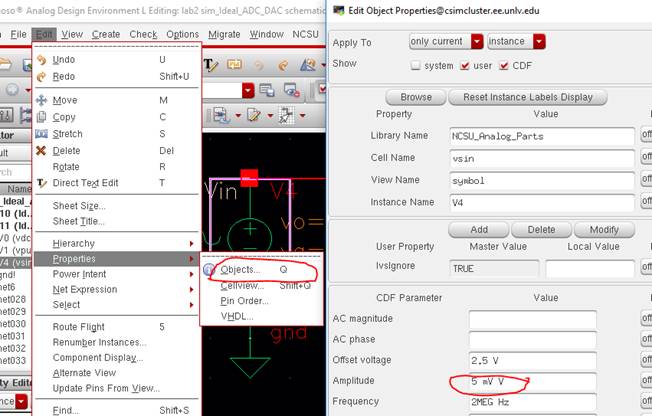
Now, press
Check and Save to make sure there are no errors, and rerun the simulation.
By pressing
the bindkey A and B on the new plot, we can draw
markers.
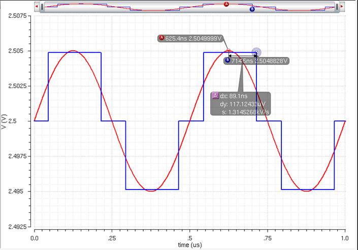
As Vin goes up
to about 5mV, Vout steps up by one, or one bit. The value
of the step is 2.50488 – 2.5 = 4.88mV, and thus proving the step size.
To Verify
again, lets make it to where the input DC offset is equal to 2.44 mV, and the
AC amplitude is also 2.44mV, so the max amplitude is 4.88mV.
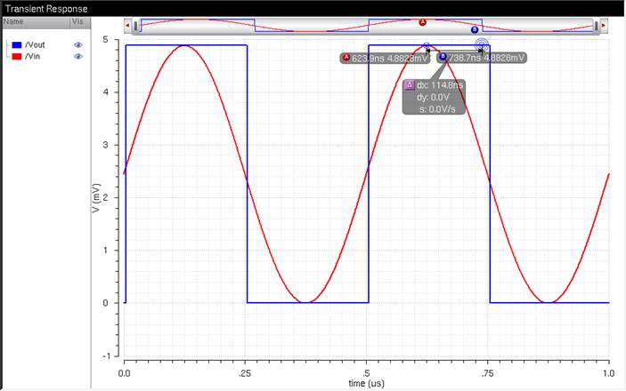
Now that’s definitely the right step size of 4.88mV.
--------------------------------------------------------
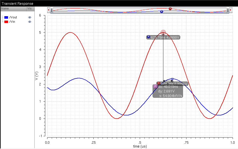
Experiment 1: Creating a
Digital-to-Analog Converter
For this, we
will first create a new schematic by clicking on the top of the Schematic
Editor and clicking on “New”.
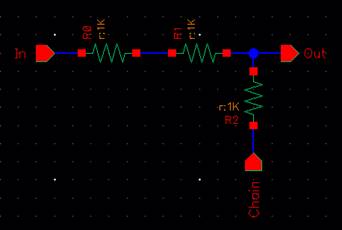
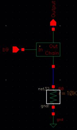
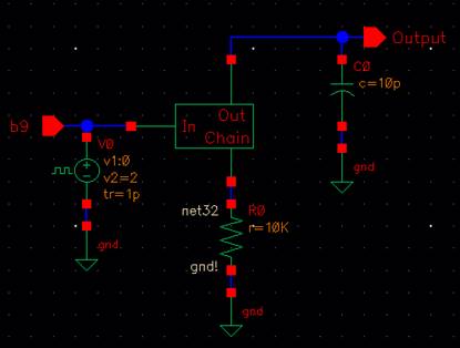
The following circuit
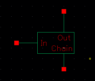
will be created, where R = 10kΩ.
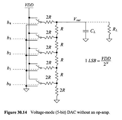
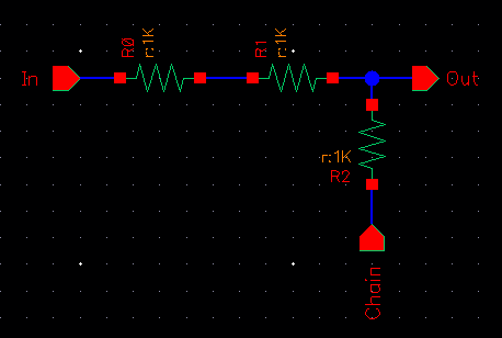
Since there is
a lot of resistors, and we want to find an easy way to chain a lot of them,
this above circuit will be our module.
To create a
module, we will be clicking on the top of the schematic Create -> Cellview -> From Cellview
And creating
the module under whatever library you choose (you can use lab2’s library or
create your own).
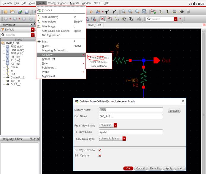
On the next
window that appears after pressing OK, set your pins to however you want to,
for this example, I will place my pins as follows:
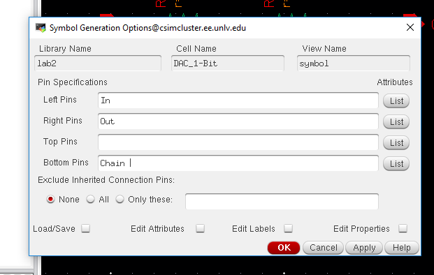
Click OK. Now
we can edit the following symbol to make it small and neat.
-
Note, to rotate something, press bindkey R to bring up the rotate menu!
-
Also note that I rotated my “Out” pin,
so it wont match the above pic .-.
Check and save,
and lets create another symbol, using a new schematic
and build a 10-bit DAC (repeat above process).
To use your
new symbol, press bindkey I, and locate the library
that you have saved it in the component browser (for this example, I saved it
to Lab2 library).
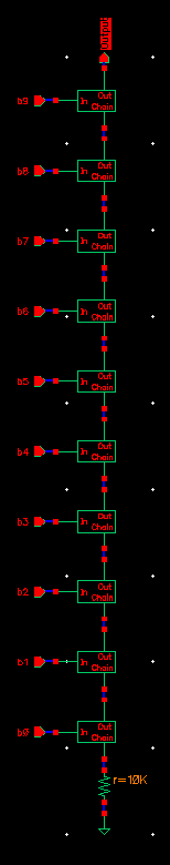
Don’t forget
to add a 10kΩ resistor at the bottom! (Also, create pins!) (Note, GND Pin
is not necessary)
Check and
Save.
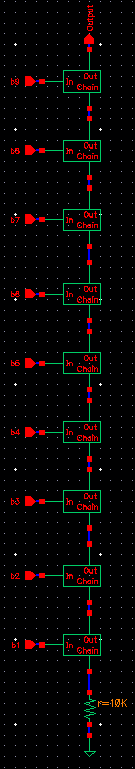
Now, to reuse
the symbol that was used for the Ideal 10-Bit DAC, under its cell, right-click
on the symbol and Copy it to your 10-bit DAC schematic.
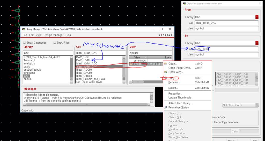
After that,
you may freely edit the Schematic.
After renaming
the pins, this is my result:
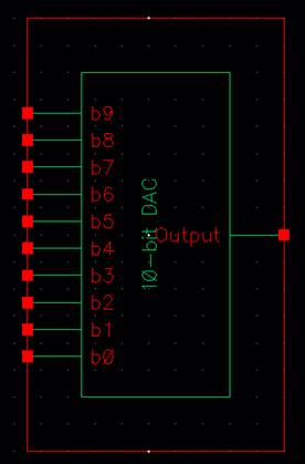
Output Resistance:
To calculate
the Output Resistance, we will ground All inputs b0-b9 and combine the
resistors in parallel and series. In the module, between the input and output,
we have a resistance of 2R. From the chain to the output, we have a resistance
of R. The input to the bottom chain is R, so for the bottom module, b0, we will
have 2R at the very bottom of the 10-bit DAC.
2R (from the
grounded IN to the OUT) in parallel with 2R (from the very bottom resistor to
OUT), we will have a resistance of R.
 …
…
Final output
resistance: R = 10kΩ
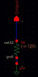
Delays:
We will be
looking at the DAC and grounding every pin except for b9 and the output. We
will place a 10pF capacitor at the output and seeing the delay.
Quick
Hand-Calcs
Theoretically,
a capacitor and a resistor in series will give us an RC time constant. The
formula for this is Vout = Vin x (1 – eT/(RC)), where RC = Time constant.
For one time constant (So, RC = T), Vout will equal 63% of Vin.
The time for Vout to be half of Vin is about td = .7RC = 70ns
So since C = 10pF, and the resistance looking at the output of the
DAC is 10kΩ,
the time constant should be 100ns
Launching the
Analog Design environment and setting a new transient analysis:
In this
simulation, the following circuit (at a low-level view) is:
This is
basically a voltage divider, so the output’s max voltage is half of Vin.
With Vin = 2V,
Max Vout = 1V
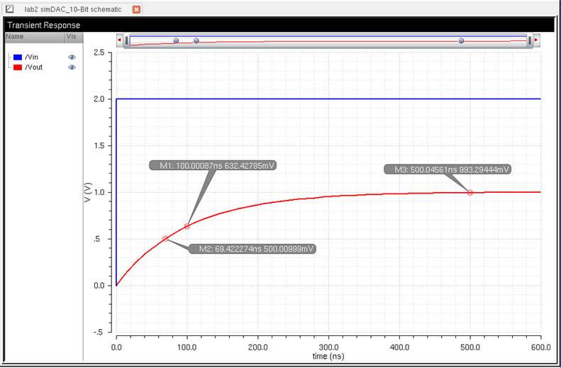
The time
constant voltage at 100ns is 632mV, or 63%
of the max Vout=1V.
The time delay
at half of the max of Vout is 69.4ns, which is close to the hand calcs.
Simulations:
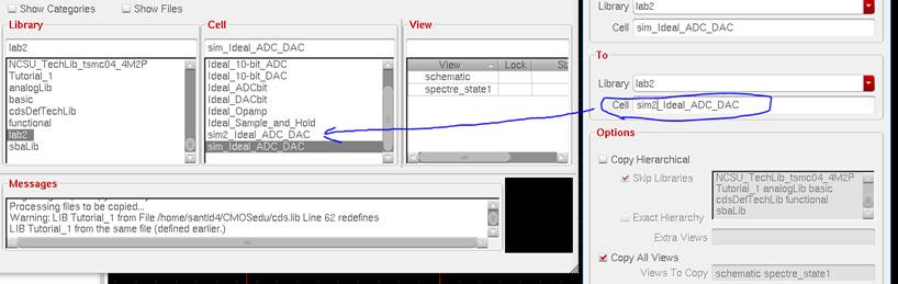
Now, we will
copy the first sim, sim_Ideal_ADC_DAC, to a new
cell sim2_Ideal_ADC_DAC, and
replace the Ideal DAC with our own.
Simulation Results:
Assuming you
loaded the same state, this is probably what you’ll have. It’s incomplete, and
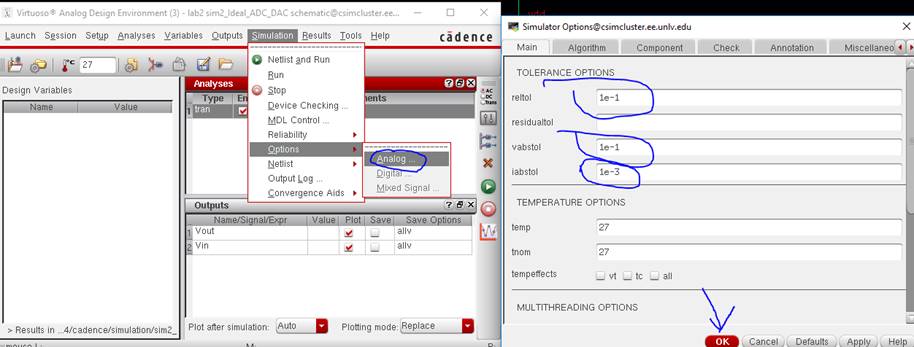
to fix this, In the ADE, go to: Simulation -> Options -> Analog, and type
into the boxes the following picture:
Reltol = 1e-1, Vabstol = 1e-1,
iabstol = 1e-3
New Simulation Result:
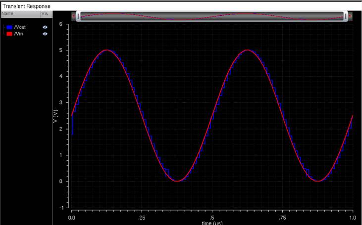
The DAC works
and we can move on to testing it.
Let’s us now have a Ramp function
be our new input source.
Clicking on Vsin and pressing Q so we
can rename the source to “vpulse”:
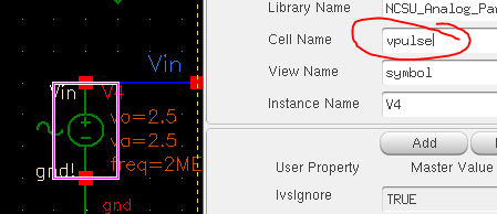
To generate a
Ramp input, we use a longer rise time of 1μ second, and our ADE transient
sim will run for just 1μ second.
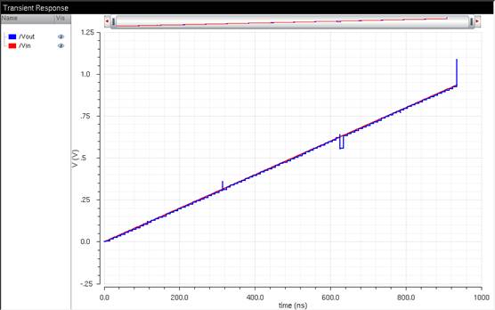
Zooming in:
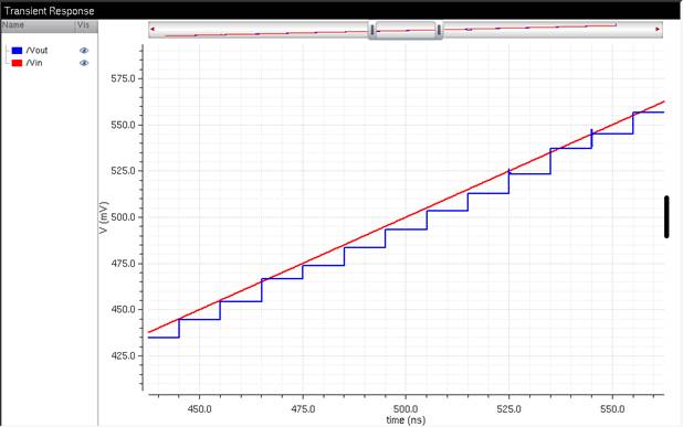
We can see
that the output is going up in steps and that there are some “glitches” when
running the ramp function. The zoomed picture also shows that the output is quantized, or values that look
discrete.
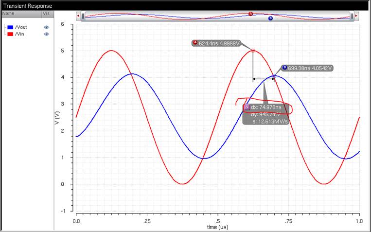
Experiment 2: Driving Loads
We will first
make the ADC to DAC circuit drive a 10kΩ Resistive load.
Results:
Adding a
resistor to the output and having half the voltage of the input means that the
whole ADC to DAC circuit is basically equal to the resistor 10kΩ. This
verifies that the DAC’s output resistance is 10kΩ.
Now lets replace this resistor with a
capacitor of 10pF.
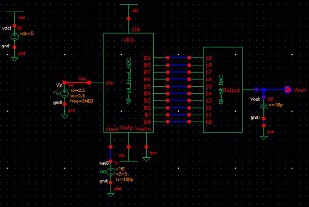
Results:
With the 10pF
Capacitor, we get a smooth curve but with a delay that is around 70ns.
Lets now have both the capacitor and resistor connected at the same
time.
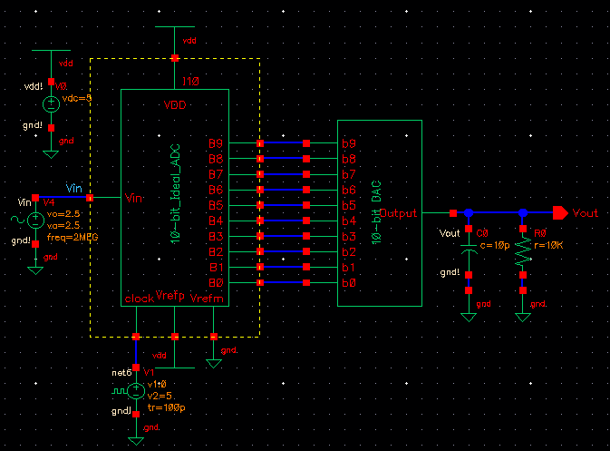
From this, we
get about half the original signal due to the Output resistance and the Load
Resistor being a Voltage divider, and the signal is smooth and delayed by about
55ns due to the capacitor and the Time Constant.
Conclusion:
We can say
that the resistor equal to the Output Resistance of the DAC will make the
Output Voltage drop, however a
Resistive Load and No-Load will make the output be in phase with the Input.
A pure Capacitive
Load will make the signal smooth and lag a lot, but introducing a resistive
parallel component will
In a real
circuit, the Switches that are seen in the following diagram, are actually implemented with MOSFETs.
These MOSFETS
should have a very small output resistance so that we can ignore their
parasitic impedance.
-
If the Output Impedance of the MOSFETS are NOT Small, then the MOSFETs will add a resistance to the 2R
resistor and then the output Resistance will be higher due to the parasitic resistance.
We would need to recalculate the Output Resistance of the DAC so that we can
find the max load resistance for the voltage divider.