Lab 7 - EE 421L
Authored
by Staford Snow, snows4@unlv.nevada.edu
11/15/2016
Lab
description:
In this lab, I learned about utilizing buses and arrayed
symbols in our designs to make schematics concise and easier to
use. I then used the
buses and arrayed symbols to create 8-bit gates including: NAND, NOR,
AND, OR, and inverter. Afterwards I created an 8-bit wide word
2-to-1 DEMUX/MUX and full adder.
Pre-Lab:
Following the lab instruction, I backed up all my work from the lab and course, read through the entire lab, and went through Tutorial 5.
Lab:
To start the lab,
I followed the instructions for how to create a 4-bit inverter.
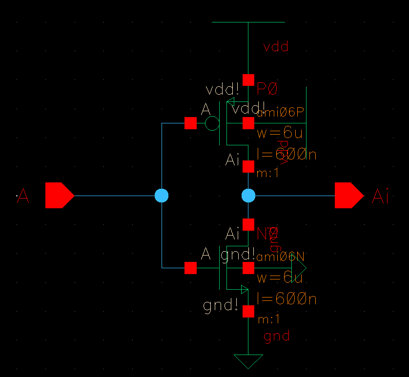
First, I created a the schematic and symbol for a 6u/6u inverter.


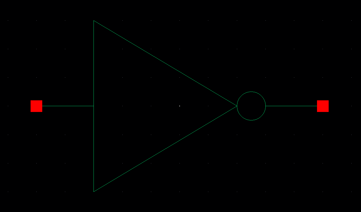
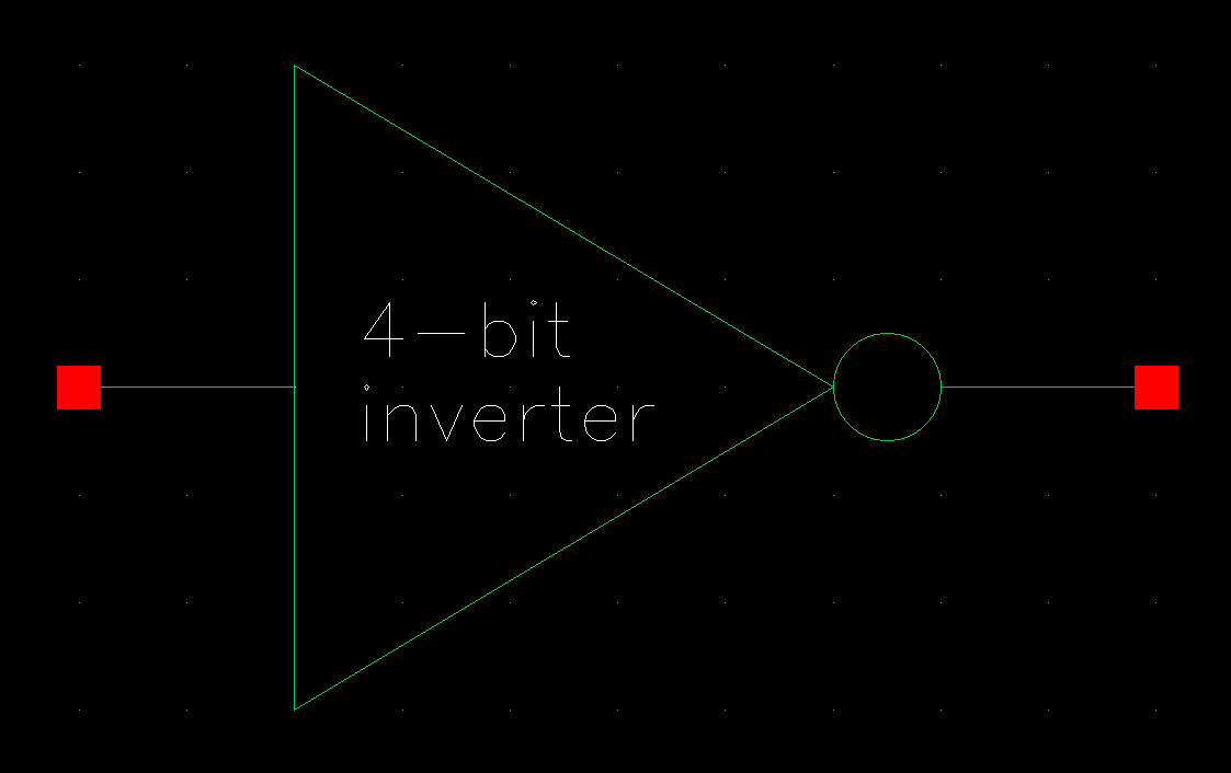
I then used an array of this symbol to draft a schematic and symbol for the 4-bit inverter.

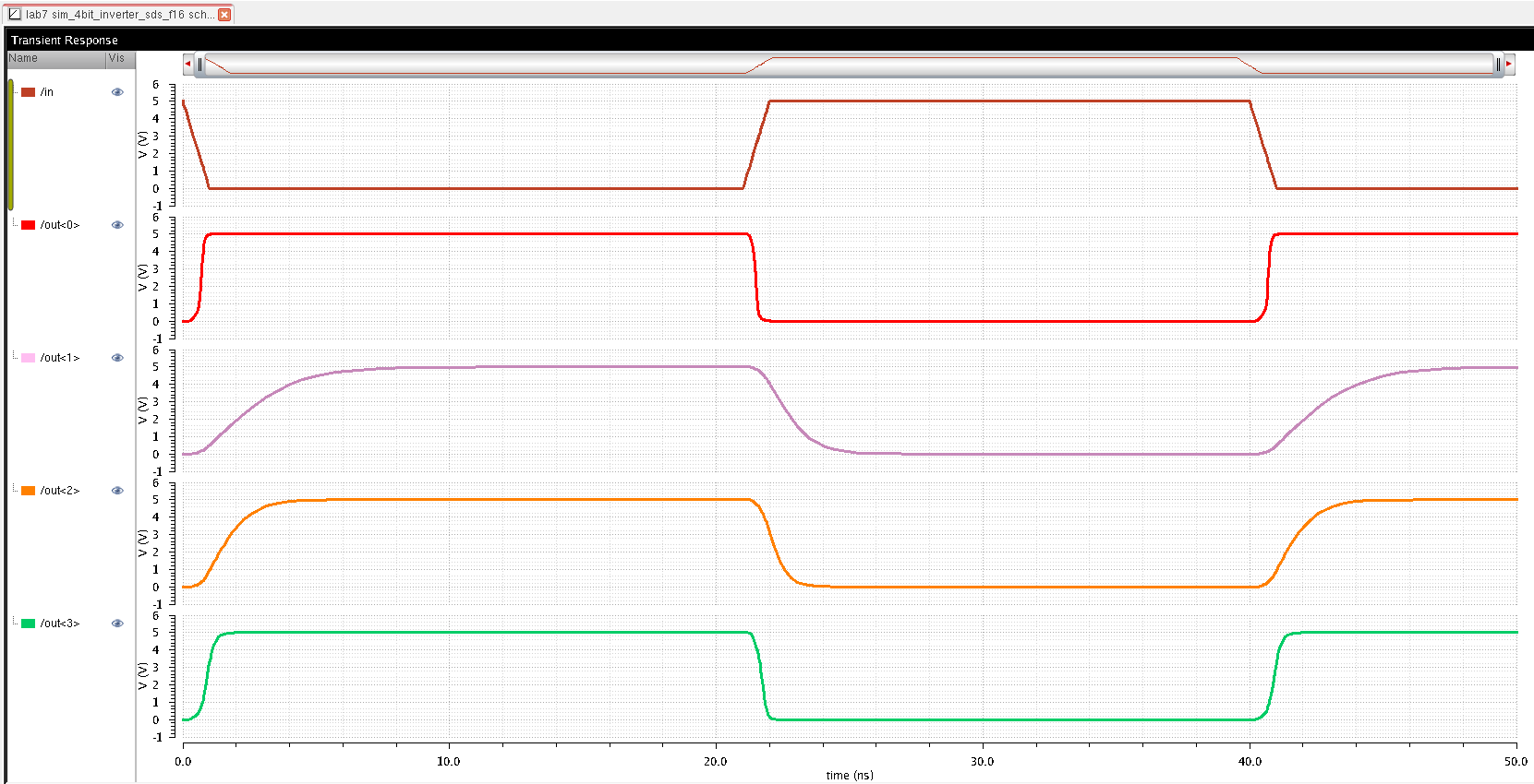
After finishing the 4-bit inverter, I set up a schematic to simulate the operation of the inverter.
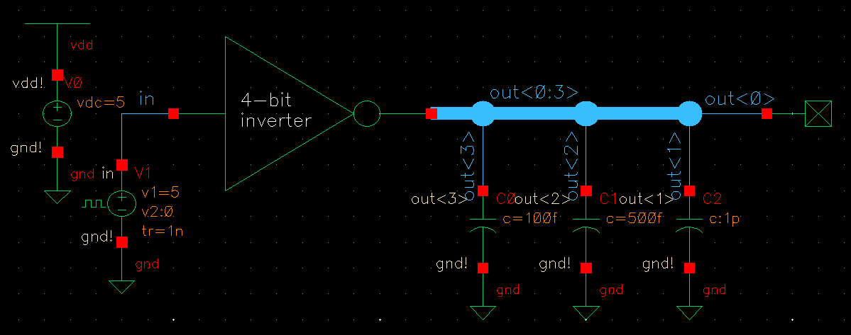
This simulation circuit generated the following graphical output:
The
varying capacitive loads on the inverter changes the switching delay of
the inverter. As the capacitive load increases, the rise/fall
time increases proportionally.
After creating and simulating the 4-bit inverter, I
began the design of the 8-bit NAND, NOR, AND, OR, and inverter. I
adjusted the process I had just learned to be used to create 8-bit
gates.
I combined these 8-bit gates into one schematic to simplify simulation.
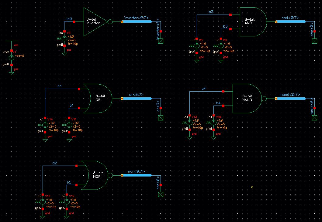
After simulation, I derived the following graphical output:
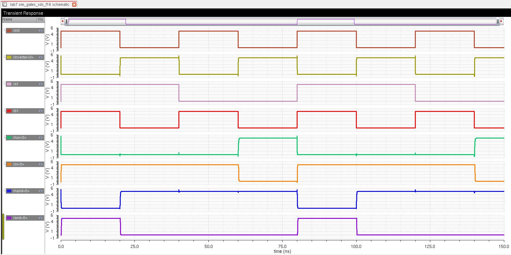
The next schematic and symbol I was instructed to draft was of a 2-to-1 DEMUX/MUX.
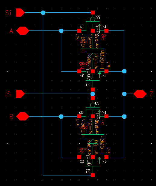
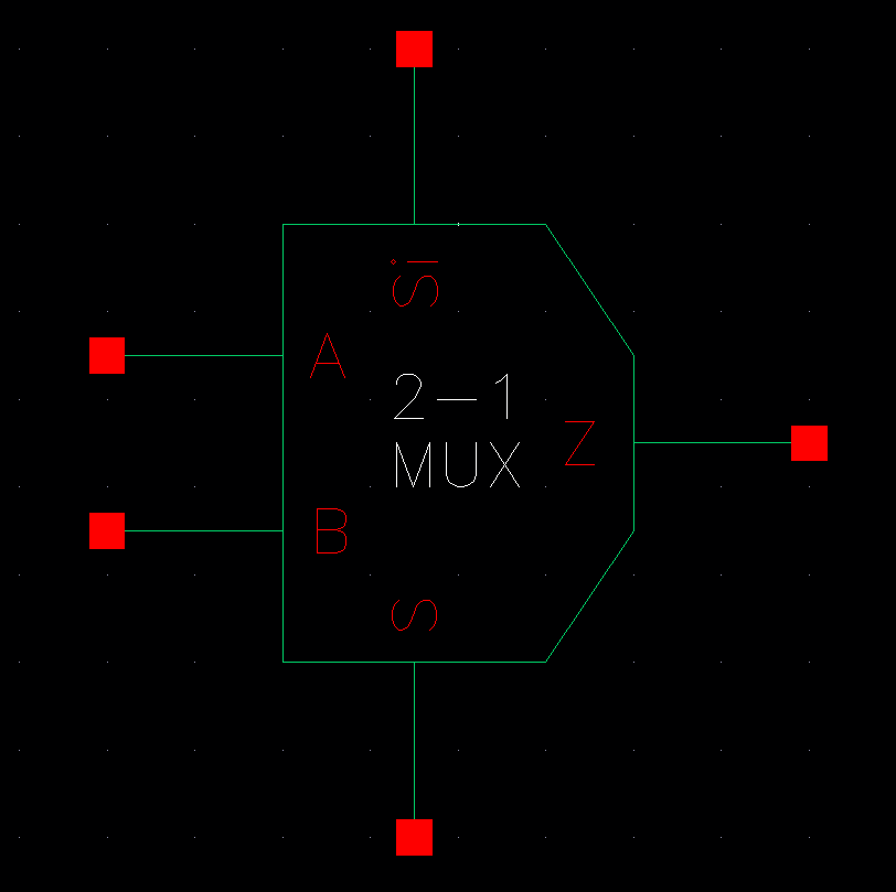
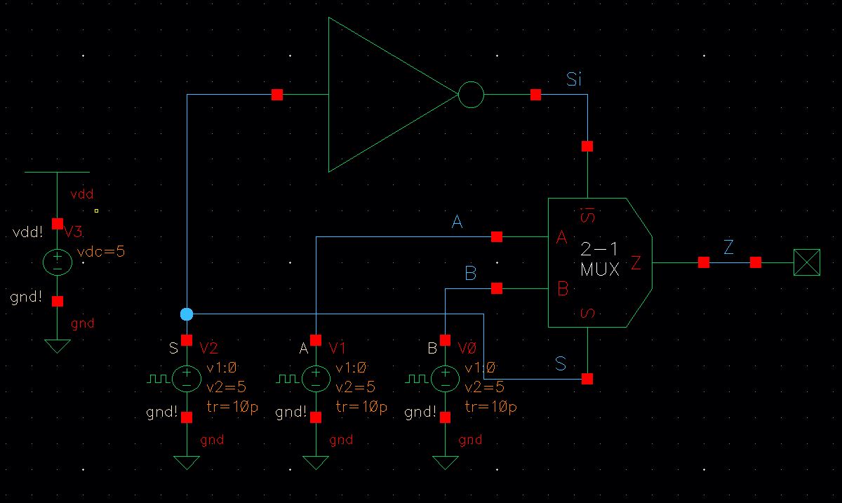
I created the following schematic to simulate multiplexing:
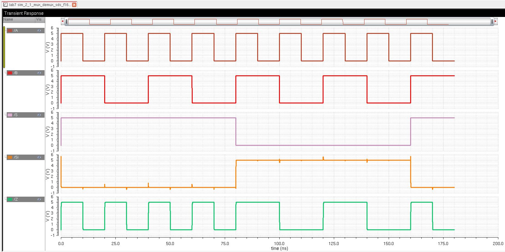
Which gave this graphical output:
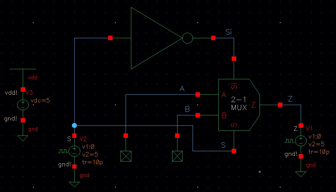
To simulate de-multiplexing, I drafted this schematic:
Which produced this output:
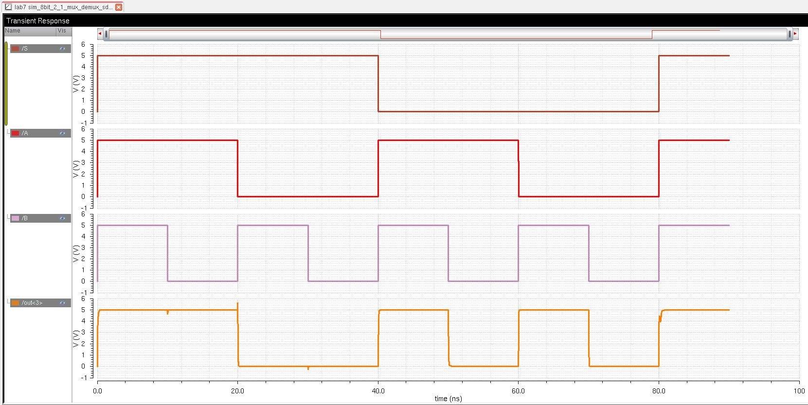
The
DEMUX/MUX works by setting the S/Si inputs to either decide whether
input A or B is let through to Z while MUX-ing, or to select whether Z
will output to A or B while DEMUX-ing.
I
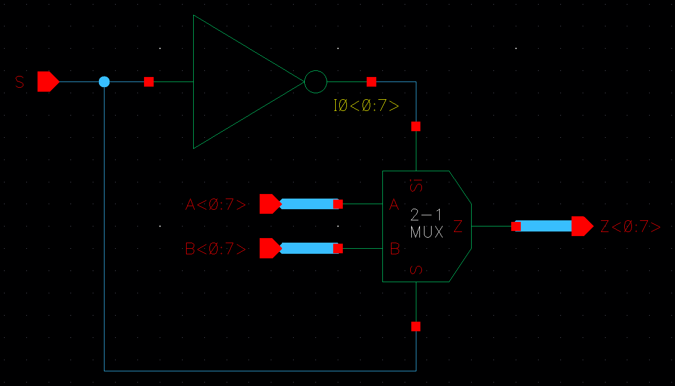
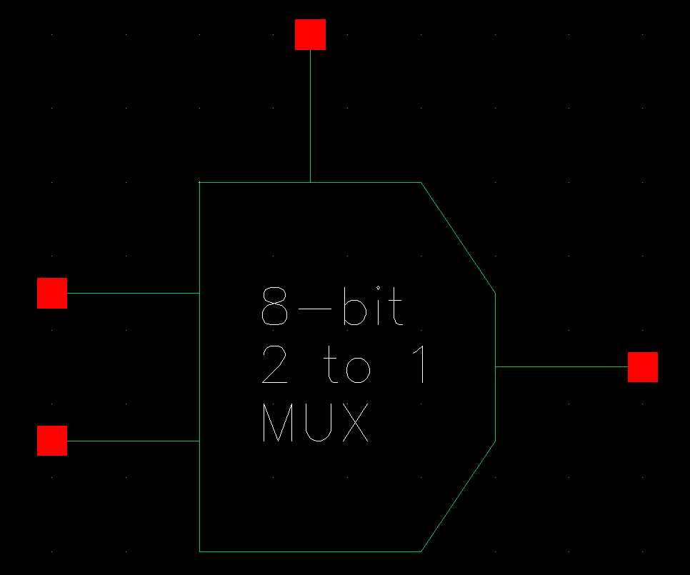
next created an 8-bit wide word 2-to-1 DEMUX/MUX schematic and
symbol. I included an inverter in my schematic to the finished
cell only needs one select input.
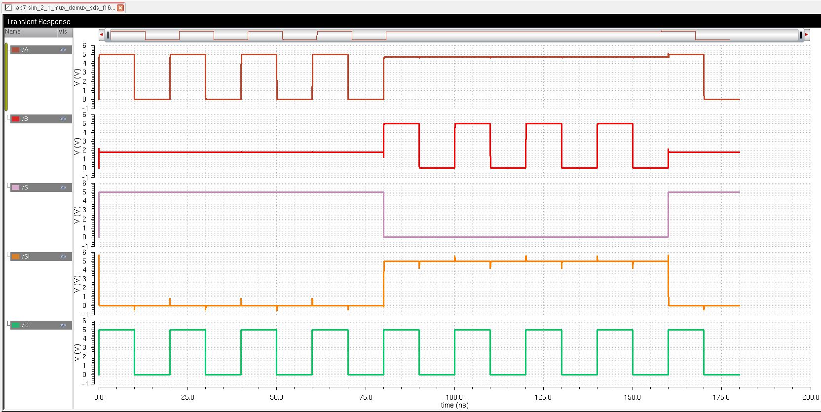
I then drafted a schematic to perform simulation of the 8-bit wide word DEMUX/MUX.
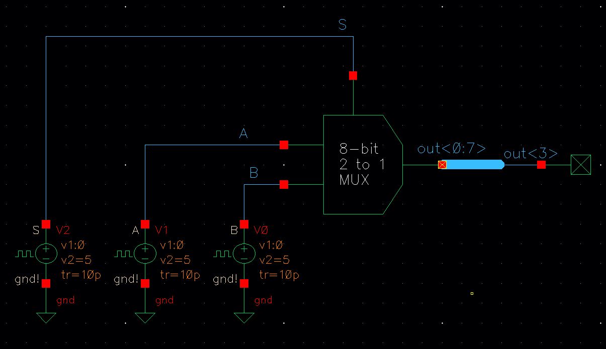
The simulation generated the following graphical output:
The
final part of the lab was to draft the full-adder schematic shown in
Fig. 12.20 in the book. I was instructed to use 6u/0.6u sizes for
both the PMOS and NMOS.
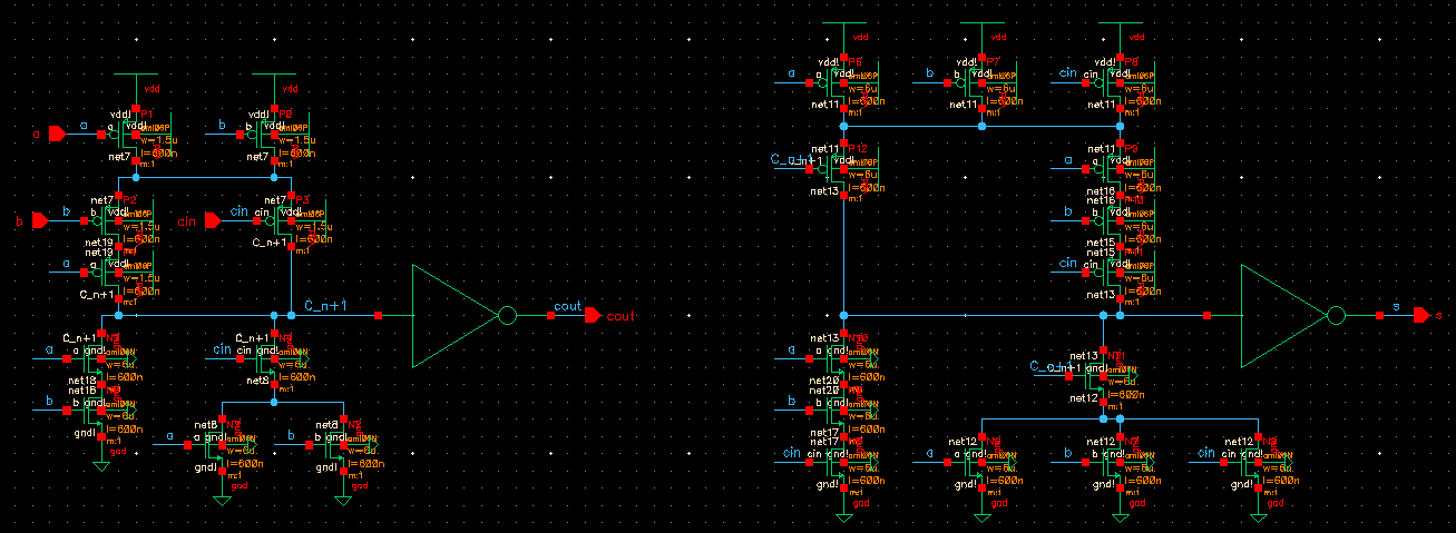
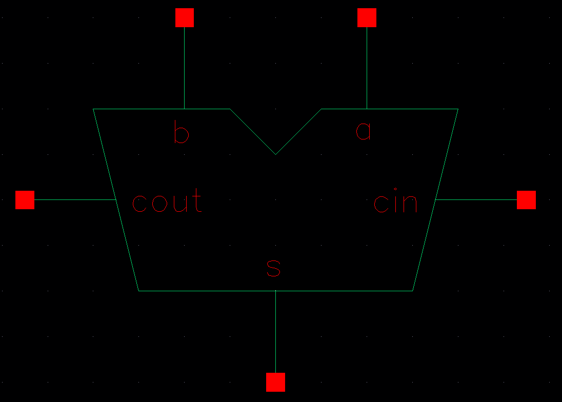
I then created a symbol to represent this schematic.
I made an array of this symbol to represent an 8-bit full-adder in a schematic and symbol.
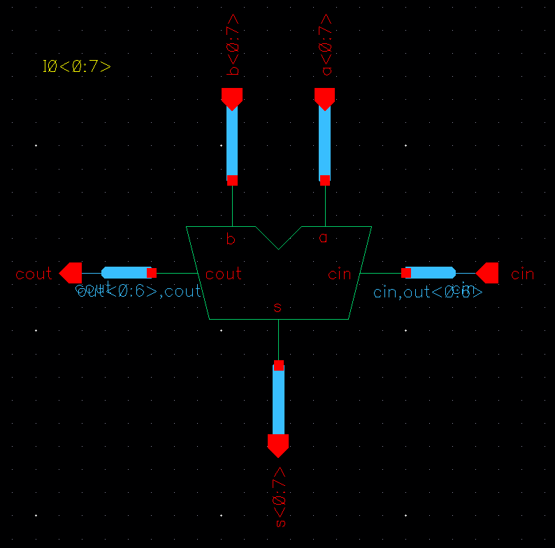
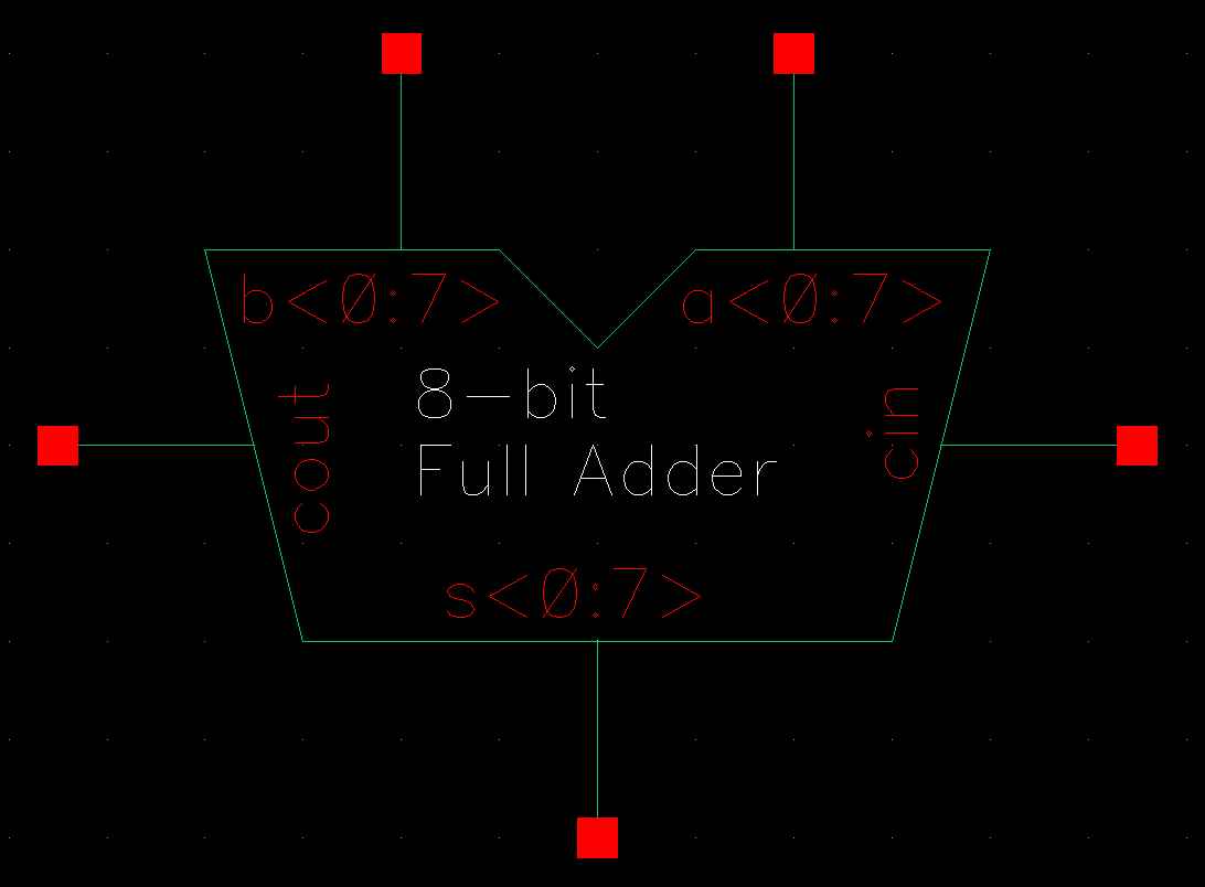
I
labeled the buses on cin and cout to loop. Cout of the
first full-adder was connected to cin of the second full-adder and so on for all 8 full-adders.
I created a schematic to simulate the 8-bit full-adder.
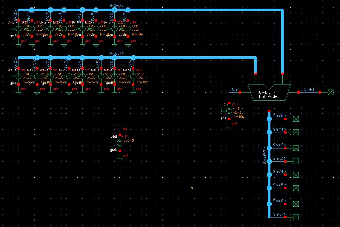
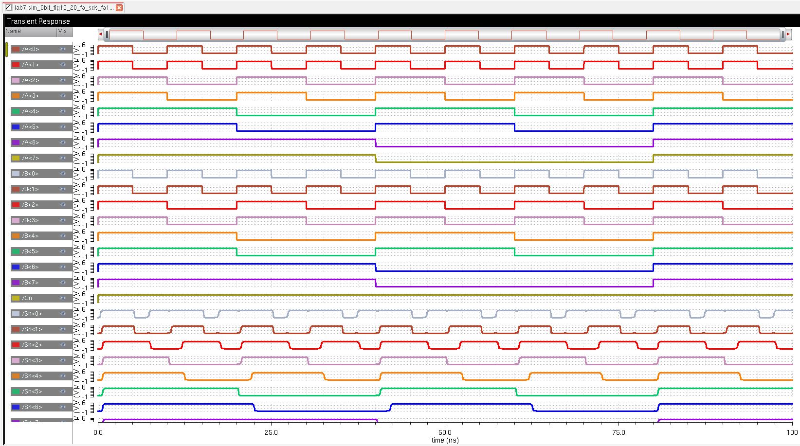
After simulating, I was able to verify the 8-bit full-adder worked correctly.
Lastly, I created a layout of the 8-bit full-adder.

A closer view of each individual full-adder is below:
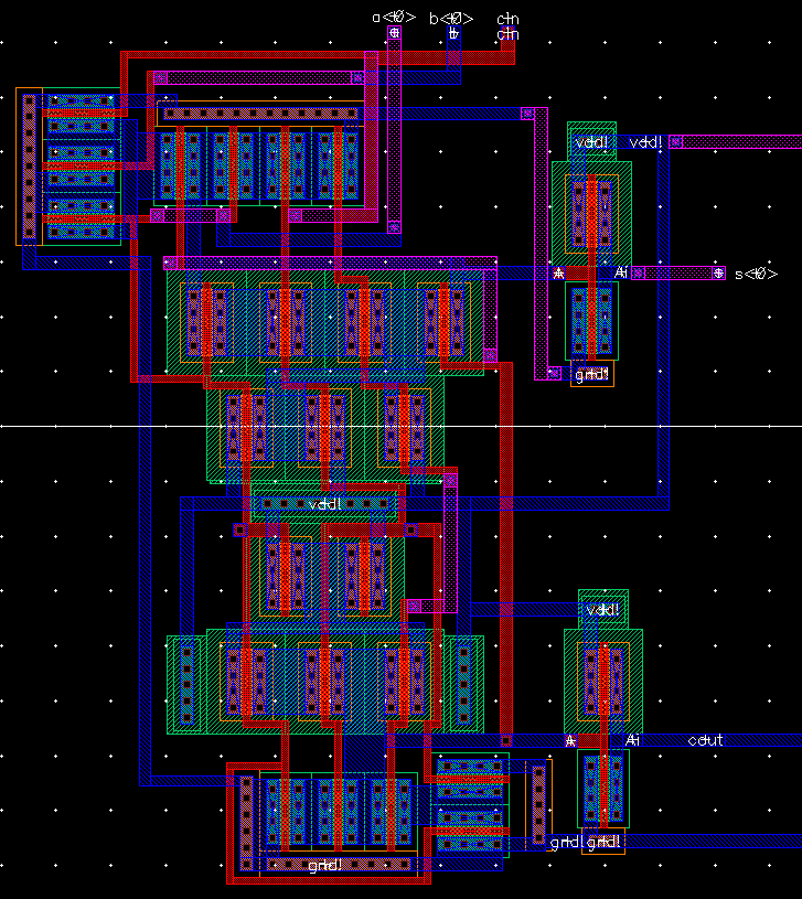
This layout successfully passed DRC and LVS.

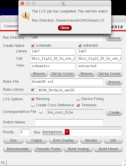
This concluded the requirements for lab 7. I have included a zipped file of the library here.
Return to my labs
Return to EE421L
