EE 421L Digital Integrated Circuit Design
Laboratory - Lab 4
9/28/16
Pre-Lab
o
o Back-up all of your work from
the lab and the course.
o Read through this lab before
starting it.
o Go through Tutorial
2
o In the simulations in this lab
the body of all NMOS devices (the substrate) should be at ground (gnd!) and the body of all PMOS devices (the n-well) should
be at a vdd! of 5V.
The prelab following Tutorial 2
required creating NMOS and PMOS layouts and simulating the IV curves for each
device via parametric analysis. These files were then transferred to the Lab 4
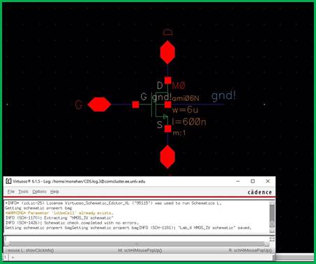
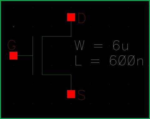
file and used to perform the simulations. First the NMOS schematic, below left,
and symbol, below right were designed with a DRC to verify design rules were
followed. Note the proper dimension 6um/600nm, displayed on both views.
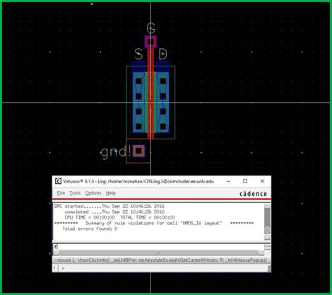
Next, the NMOS layout, below left,
and extracted, below right, views were created with both DRC and LVS
verifications to ensure proper design.
Simulations were performed as
required by Tutorial 2, but these are similar to the simulations required in
Experiment 1 below, thus these will be omitted from the PreLab
summation and included below. Following the NMOS design, the same procedure was
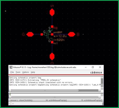
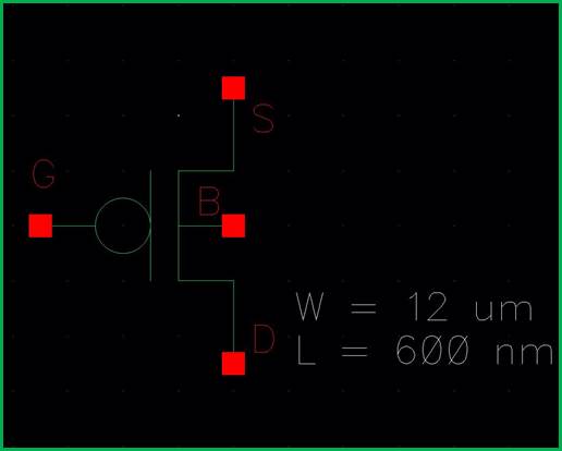
completed for the design of a PMOS. The PMOS schematic is displayed to the left
below and the PMOS symbol is displayed to the right below.
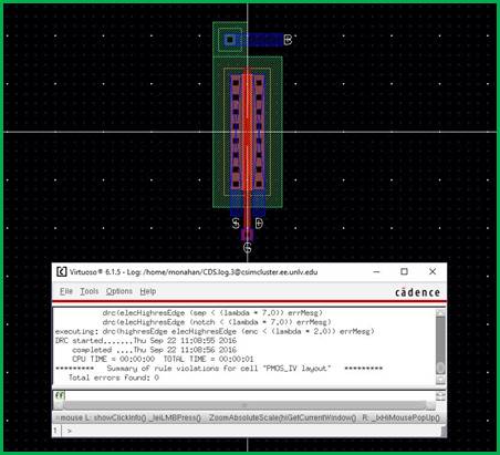
Next, the PMOS layout, below left, and
extracted, below right, views were created with DRC and LVS verifications.
Following the instructions in Tutorial 2 resulted in the successful design of
both NMOS and PMOS devices. The next step was to begin the experiments outlined
in the Lab 4 instructions.
Experiment
1
Generate
4 schematics and simulations (see the examples in the Ch6_IC61 library, but
note that for the PMOS body should be at vdd! instead
of gnd!):
o A schematic for simulating ID
v. VDS of an NMOS device for VGS varying from 0 to 5 V in 1 V steps while VDS
varies from 0 to 5 V in 1 mV steps. Use a 6u/600n width-to-length ratio.
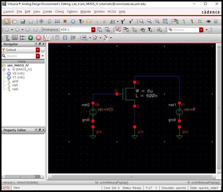
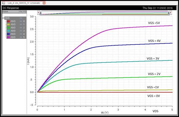
The simulation was performed as
outlined in Tutorial 2 with results matching the expected outcomes for the
NMOS. All files from the Tutorial 2 library were copied into the Lab 4 library
and used for designing the required schematics. The schematic is displayed
below to the left and the parametric analysis sweeping VGS from 0V to 5V in 1V
steps is displayed to the right. Note the NMOS used in the schematic is the
same as the NMOS designed in the PreLab. As seen
above in the NMOS schematic, the substrate is tied to ground as necessary.
o A schematic for simulating ID
v. VGS of an NMOS device for VDS = 100 mV where VGS varies from 0 to 2 V in 1
mV steps. Again use a 6u/600n width-to-length ratio.
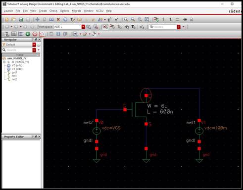
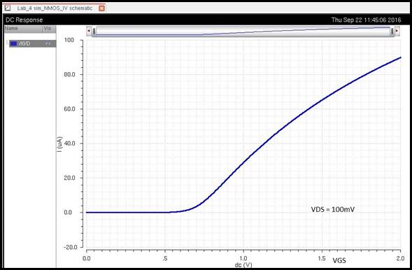
The first step in performing this
simulation required changing the voltage for VDS on the schematic to
100mV. Next, the component name used in
the DC analysis was changed to V0 to match VGS. Last, the start, stop and
step-size for VGS were edited to match the required values above. The resulting
schematic is displayed to the left below and the simulation result is displayed
to the right. The plot shows a current of zero until VGS is greater than the
threshold voltage. At this point, a relatively linear increase in current is
displayed matching expected results.
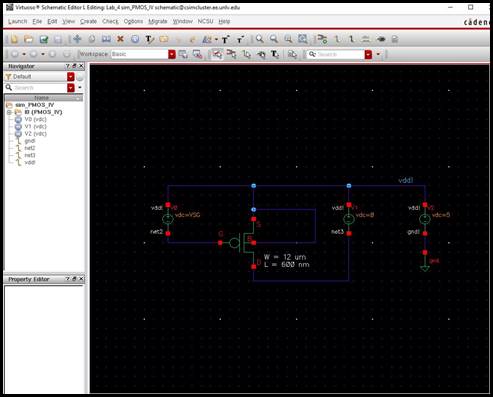
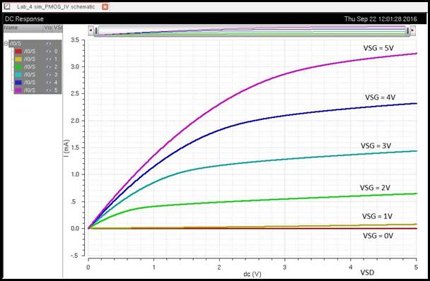
o A schematic for simulating ID
v. VSD (note VSD not VDS) of a PMOS device for VSG (not VGS) varying from 0 to
5 V in 1 V steps while VSD varies from 0 to 5 V in 1 mV steps. Use a
12u/600n width-to-length ratio.
This simulation was similar to the
first simulation performed for the NMOS and resulted in a similar I-V curve.
The PMOS schematic is displayed below to the left and the simulation waveform
is displayed to the right. Note the proper W/L as outlined in the above
instructions and the PMOS substrate tied to Vdd as
required for the device to function as expected.
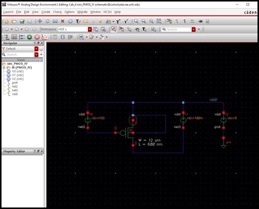
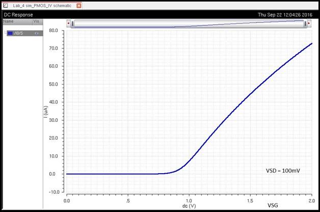
o A schematic for simulating ID v. VSG of a PMOS device for VSD = 100 mV where VSG varies from 0 to 2 V in 1 mV steps. Again, use a 12u/600n width-to-length ratio.
Again, this simulation was similar to
the simulation performed for the NMOS with the result of the PMOS exhibiting
similar I-V characteristics to the NMOS. The schematic is displayed below to
the left and the plot is displayed below to the right.
Experiment
2
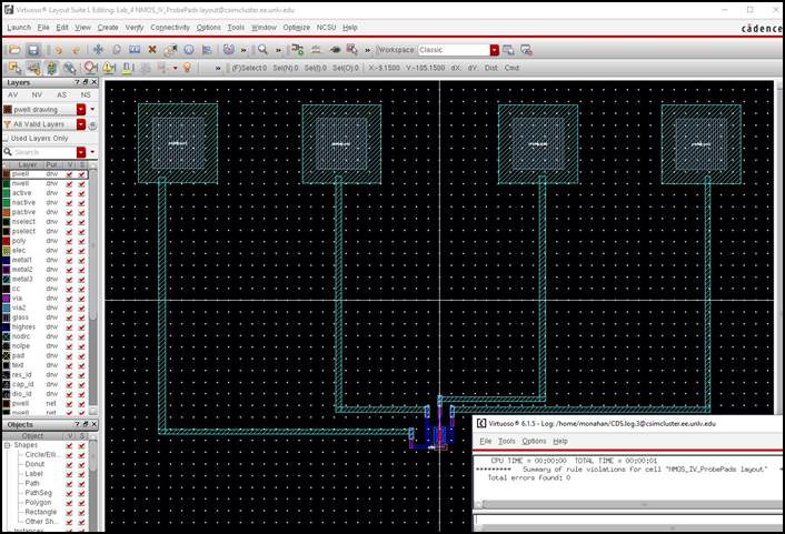
Lay
out a 6u/0.6u NMOS device and connect all 4 MOSFET terminals to probe pads
(which can be considerably smaller than bond pads [see MOSIS design rules] and
directly adjacent to the MOSFET (so the layout is relative small).
o Show your layout passes
DRCs.
o Make a corresponding schematic
so you can LVS your layout.
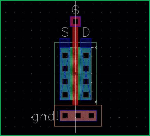
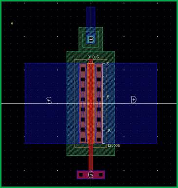
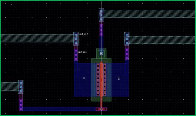
The layout of a 6u/0.6u NMOS started
with a simple redesign of the NMOS_IV cell created in the prelab. Specifically,
two extra rows were added to the p-tap to create additional grounding contacts,
as displayed in the image to the left below. The lengths of the NMOS remained
unchanged to match the required specifications for this experiment. After
instantiating the NMOS in the cell titled NMOS_IV_ProbePads, the four
probe pads and the m2_m1 and m3_m2 cells were instantiated. The metal
connecting cells were edited to result in 3 total vias
in each connection to help lower resistance between layers. The close up view
of the NMOS with these layers is displayed to the right below.
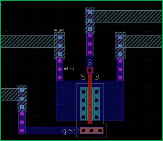
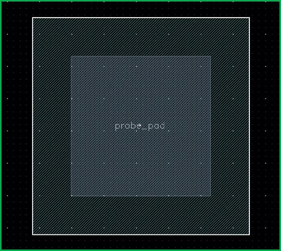
The left image below displays one of
the probe pads used to connect to the NMOS terminals. The image to the right
below displays the metal connections between the different metal layers in the
layout. This is included to demonstrate the methods necessary to connect the
metal layers.
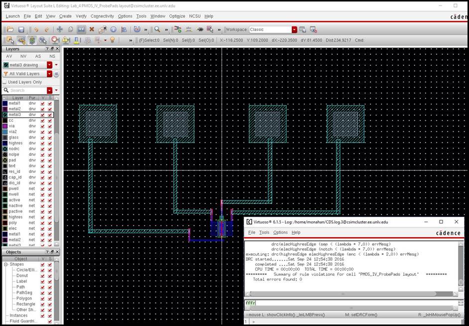
After connecting all the metal layers
and connecting to the probe pads, a DRC verification was successfully completed
as displayed below.
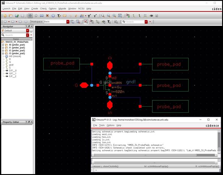
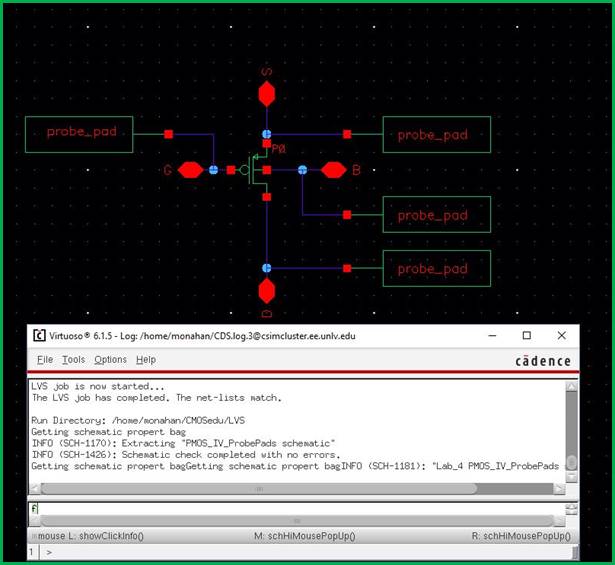
The next step required creating a
corresponding schematic to allow LVS verification. The schematic created in
Tutorial 2 was copied into the lab and probe pads were added to complete the
design. The schematic and resulting DRC verification are displayed below.
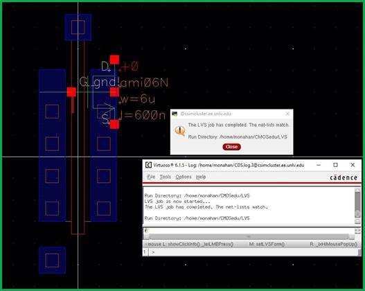
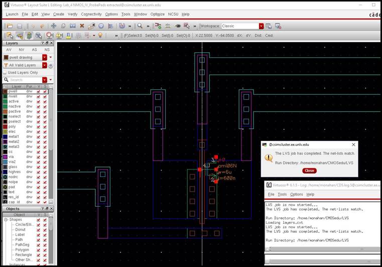
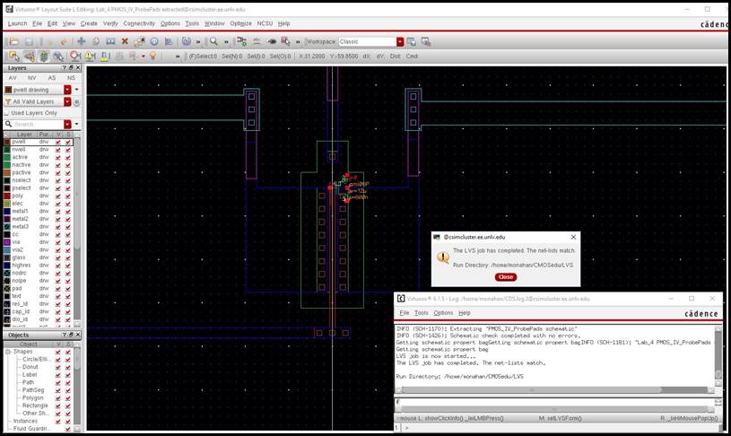
The final step in Experiment 2 was to
LVS the NMOS schematic versus the extracted layout. The image below displays a
successful LVS verification for the NMOS.
Experiment
3
Lay
out a 12u/0.6u PMOS device and connect all 4 MOSFET terminals to probe
pads.
o Show your layout passes
DRCs.
o Make a corresponding schematic
so you can LVS your layout.
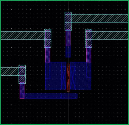
The same basic procedure was followed
to create a complementary PMOS layout with L/W = 12µm/0.6µm. The cell created
for the PMOS layout was titled PMOS_IV_ProbePads. Several vias
were added to the PMOS gate prior to instantiating to reduce resistance between
the metal contact layers, as displayed below to the left. Note the proper size
of 12µm/0.6µm displayed on the PMOS. Following the PMOS_IV layout is an image
illustrating the addition of the necessary m2_m1 and m3_m2 connections.
After completing the layout, a DRC
verification of the PMOS was performed with the successful results displayed
below.
The next step required designing the
schematic to LVS with the extracted layout. The PMOS schematic connected to the
probe pads with DRC verification is displayed below.
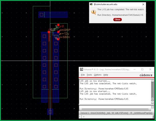
The final step in Experiment 3 was to
LVS the PMOS schematic versus the extracted layout. The image below displays a
successful LVS verification for the PMOS.
Conclusion
The experiments performed in
Laboratory 4 resulted in the successful design of NMOS and PMOS schematics and
layouts using ON's C5 process with valid DRC and LVS verifications for all
designs. Furthermore, the I-V characteristics of both devices were simulated
with results matching expected outcomes.
Return to
Monahan Lab Report Directory
Return to EE 421L
Fall 2016 Student Directory