Lab 2 - EE 421L
Prelab:
·
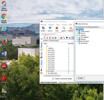
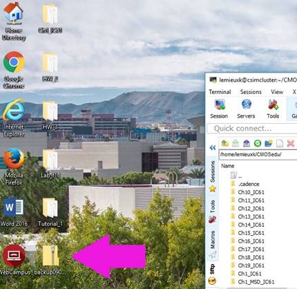
Back-up all of your work from the lab and the course.
I backed up my
work by downloading what I wanted to back up on my desktop, zipping it, and
e-mailing it to myself.
·
Read through this entire lab write-up before doing the pre-lab
·
Download lab2.zip to your desktop.
This archive
contains a simulation example using an ideal 10-bit Analog-to-Digital Converter
(ADC) and Digital-to-Analog Converter (DAC).
·
Upload this zip file to the design directory on the server that
you are running Cadence from, e.g., Tutorial_1, CMOSedu,
etc.
Note that it's
assumed you are using the NCSU Cadence Design Kits.
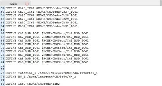
·
Unzip this directory and add, to your cds.lib in the design
directory, the following statement (assuming the design directory is CMOSedu):
·
DEFINE lab2 $HOME/CMOSedu/lab2
·
Start Cadence from the design directory.
Downloaded
lab2.zip, uploaded it to the CMOSedu directory, and
unzipped it:
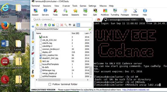
Added this to
cds.lib:
·
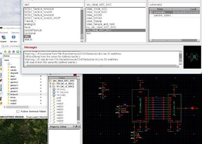
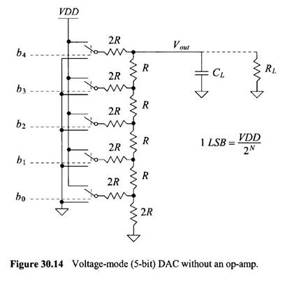
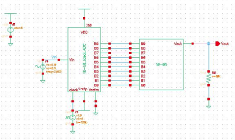
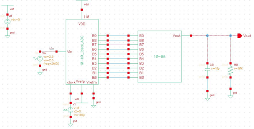
Open the schematic view of the cell sim_Ideal_ADC_DAC.
This cell
contains the ideal 10-bit ADC and DAC as seen below in the second image.
·
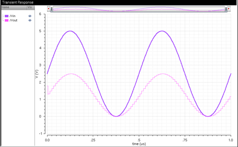
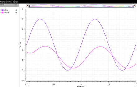
Run the simulation (Launch the ADE, Session -> Load State ->
Cellview -> OK, press the green start button) to
get the following.
Make sure you
understand how to change the background color, line thickness, and type of line
(e.g. solid, dashed, etc.)
The ADC
(Analog Digital Converter) samples a signal converting a continuous time signal
and amplitude and analog symbol to a discrete time and amplitude digital signal
with a sequence of values. Thus, the DAC does just the opposite. It takes the
sequence of bits rebuilding the signal with them. The pin B[9:0] is a discrete
time signal being a 10-bit representation of the analog signal from the ADC. By
the equation where bits are 2n, 210 is equal to 1024 bits
that is inputted into DAC by the ADC
Post lab:
·
The design of a 10-bit DAC using an n-well R of
10k
o
The 2R resistor should be implement with two separate
10k resistors in series
o
After you've designed and drafted your schematic check and save it
·
How to determine the output resistance of the DAC (answer: R)
by combining resistors in parallel and series
·
Delay, driving a load
o
Ground all DAC inputs except B9. Connect B9 to a pulse source (0
to VDD) and show, and predict using 0.7RC, the delay the DAC has driving a 10
pF load
o
Verify the simulation results match your hand calculations
·
How to create a symbol view for your design with the exact same
footprint as the Ideal_10-bit_DAC symbol view (hint: use Copy before you
start drafting your design, e.g. Copy the cell Ideal_10-bit_DAC to
Mydesign_10-bit_DAC and then simply edit the schematic view!)
o
See Tutorial
1 for additional help
o
Note that your design won't use VDD, Verfp,
or Vrefm so you can delete those pins on your
design's DAC symbol view
·
Simulations to verify your design functions correctly.
o
Copy the schematic cell view sim_Ideal_ADC_DAC to
a cell sim2_Ideal_ADC_DAC and replace the ideal DAC with the one you just
designed
o
Use the sim2_Ideal_ADC_DAC to illustrate that your design works as
expected.
o
Show what happens if the DAC you designed drives a load (both R,
C, and R/C)
o
Explain what happens if the DAC drives a 10k load?
·
In a real circuit the switches seen above (the outputs
of the ADC) are implemented with transistors (MOSFETs).
o
Discuss what happens if the resistance of the switches isn't small
compared to R.
·
If you have simulation convergence problems you can force the
simulation to converge by going to, in the ADE, Simulation -> Options ->
Analog
o
Set the values as seen below
§ relative
tolerance, reltol, of 10% (= 1e-1)
§ voltage
absolute tolerance, vabstol, of 100 mV (= 1e-1)
§ current
absolute tolerance, iabstol, of 1 mA (= 1e-3)
o
The accuracy of the simulation will, obviously, be
degraded
10-Bit DAC
Design:
First, I must
start with design my own DAC. Below shows the components needed for 1-bit as well
as the corresponding symbol.
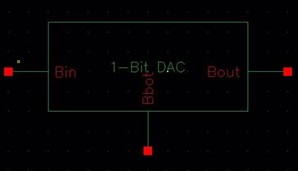
1-Bit Design 1-Bit
Symbol
Next, I made a
10-bitd DAC from the new symbol I created! Then made another symbol to
represent the 10-bit DAC.
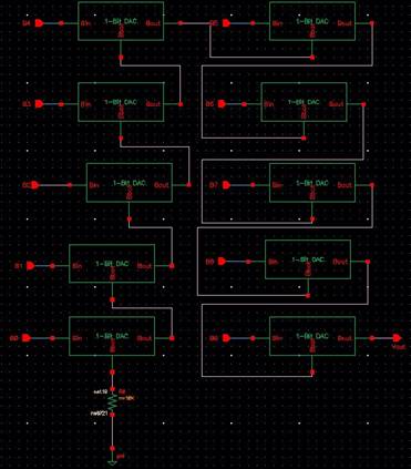
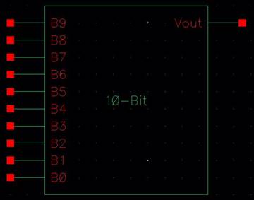
10-Bit Design 10-Bit
Symbol
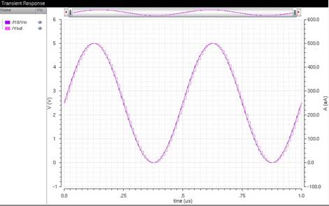
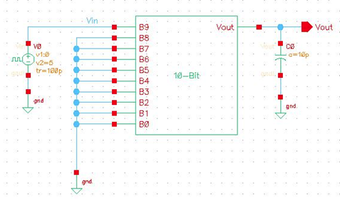
I copied the
file with the ideal ADC and ideal DAC to my own folder. I deleted the ideal DAC
and placed my very own in its place! As you can see from the schematic below,
that is a different component. Then I ran a simulation and wah
– lah! The results were as wanted; They matched the
ideal ADC/DAC nearly perfect.
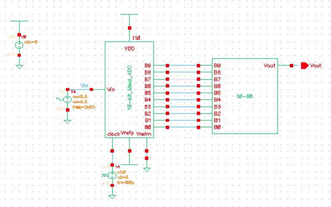
My DAC design connected to ADC and the simulation results.
Determining output resistance:
The resistor
ladder has 2R resistors in parallel with another 2R.
Equivalent
resistance:
![]() =R
=R
Throughout the ladder the R is combined in
series with R of the next bit to create another set of 2R that is parallel.
Exercise 1
-Delay, driving a load:
Connect B9 to
a pulse source, add a 10 pF capacitor, and ground all other inputs and predict
a delay driving load.
Expected time delayL
Td=0.7RC(L(L+1)/2)
where L-1, R-10kΩ, and C-10pF
Td=70ns
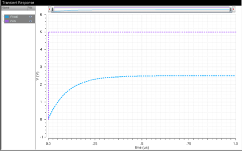
All DAC inputs are grounded except B9 that is connected to a pulse
source.
Simulations
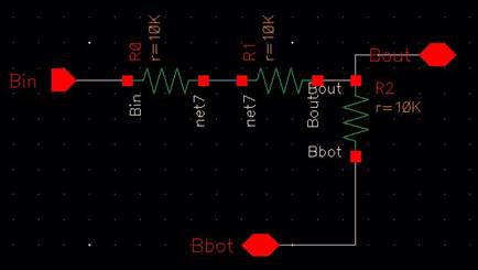
to verify:
We will now
add a resistor load of R=10k. This gives us a voltage divider of two 10k
resistors.
Vin![]() =
= ![]() Vin
Vin
The simulation
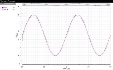
shows the output voltage being about half the input.
Resistor load
Now adding a
capacitor load, the sine wave becomes smoother and is shifted lagging the
input. See figures below.
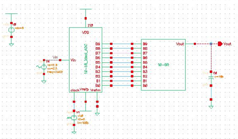
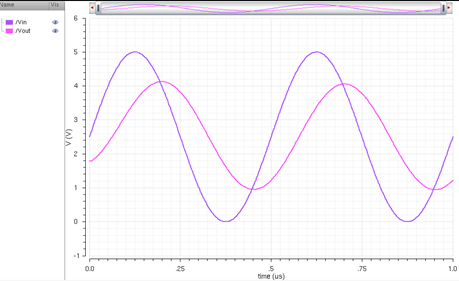
Capacitor load
The output
voltage is still lagging and gets even smaller when you add a capacitor and
resistor load to the circuit as seen below.
Resistor and Capacitor load
What happens
if the resistance of the switches isn't small compared to R?
If the resistance of the switches isn’t small compared to are then
the output resistance of the DAC will also not be so small giving rise to a
greater resistance. This will decrease in the output voltage Vout of the the DAC.