Lab 3 - EE 421L
Authored
by Martin Jaime,
email: jaimem5 at the UNLV students domain
Date: September 21, 2016
Pre-lab work:
- Back-up all of your previous work from the lab and the course.
- Finish Tutorial 1 seen here.
Lab Report
This lab will focus on the layout of the 10-bit DAC you designed and simulated in Lab 2
- Use the n-well to layout a 10k resistor as discussed in Tutorial 1.
- The
dimensions of the n-well resistor rely on the resistivity of the
material. For the C5 process, the n-well layer has an inherent
resistance of 800 Ohms / quare.
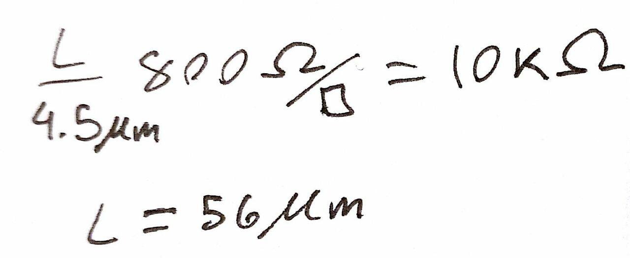
- We arbitrarily choose a width of 4.5 um (as long as it is wider than the minimum of 3.6 um for the n-well).

|
Figure 1: Hand calculations for resistor dimensions.
|
- So
the length of the resistor is 56 um. But 56/.15 = 373.3333. This length
is not on the grid as specified by the C5 process. A whole number
resulting from that division means that the measurement is within grid.
Let's force it by using 374 instead of 373.333. 374 * 0.15 = 56.1 um.
- For the width we used 4.5 and 4.5/.15 = 30 so we are okay there.

|
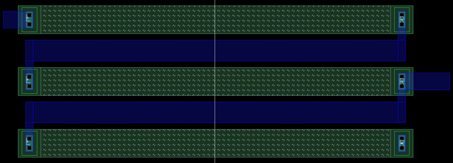
Figure 2: Layout of an n-well 10K resistor.
|
- Use this n-well resistor in the layout of your DAC
- Discuss, in your lab report, how the width and length of the resistor are measured
- Ensure
that each resistor in the DAC is laid out in parallel having the same
x-position but varying y-positions (the resistors are stacked)
- 31
resistors are necessary for implementing the 10-bit DAC. After
instantiating one n-well resistor, copy 30 more into columns, as
depicted in Figure 3.Press 'k'
while in copy mode to instantiate a ruler. Place a ruler measuring 5.4
units (the minimum distance between n-wells) from the first resistor to
place the next n-well there. Do the same one last time todetermine the distance of the rest of the
resistors. They will automatically hold the distance of the second
ruler (you will have to do some guess work since the copy instances
that dragged disappear while holding a ruler).

|
Figure 3: Copying cells
|
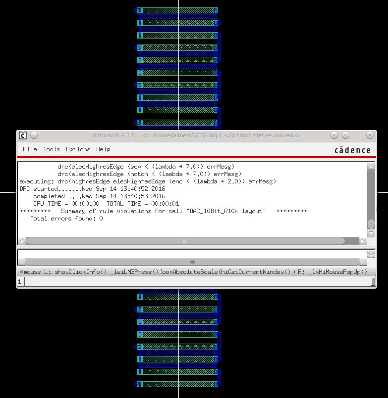
- Figure 4 illustrates all
the laid out resistors: the DAC that passes the Design Rule Check (DRC)
with routed metal1 connections between the pins of the resistors. On
the left, are the 10-bit input pins, and on the top right is the analog
output. All input and output Pins are on metal 1.

|
Figure 4: Layed out DAC with passing DRC.
|
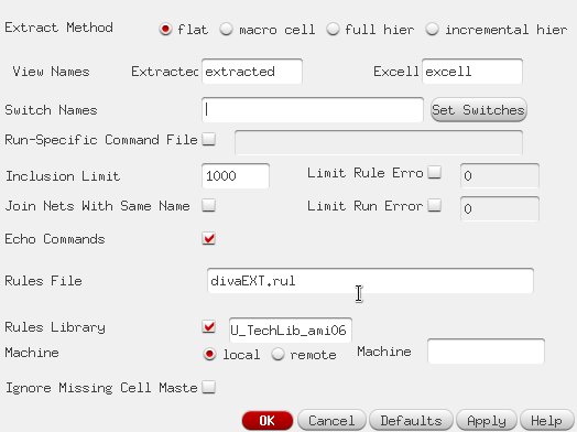
- Once
the DRC passes, extract the layout for a Layout Versus Schematic
verification. In the layout view window, go to Verify > Extract. See
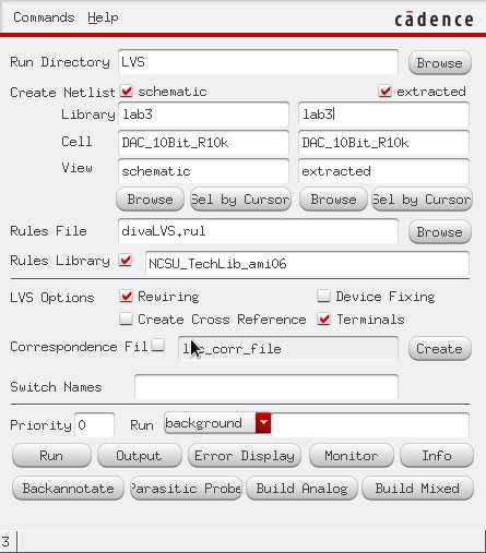
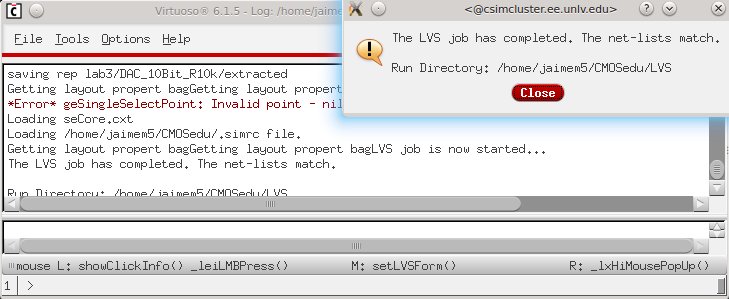
Figure 6(a) for the required settings. Click "Ok" to begin the extraction. Then, go through the menus Verify > LVS. See Figure 6(b)
for the LVS window. After it is finished processing, a pop up will
notify the user that the netlists match if they pass verification. This
message can also be verifiedin the Command Interpreter Window seen in Figure 6(c).
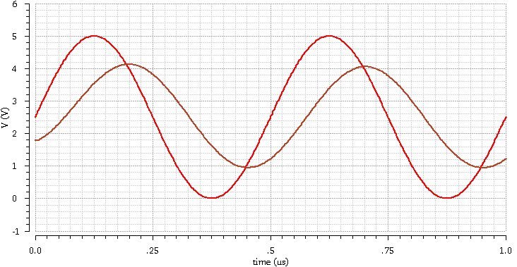
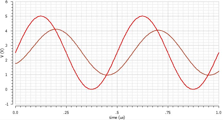
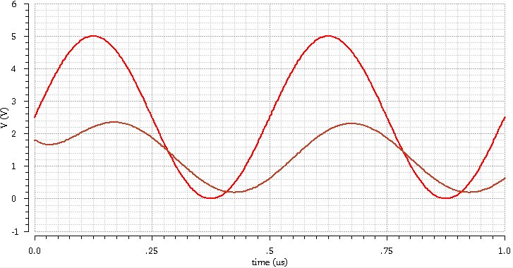
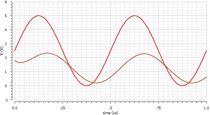
- Simulation:
- in
ADE L, go to Setup > Evironment. In the "Switch View List" menu
entry, type in "extracted" before the word "schematic" to simulate the
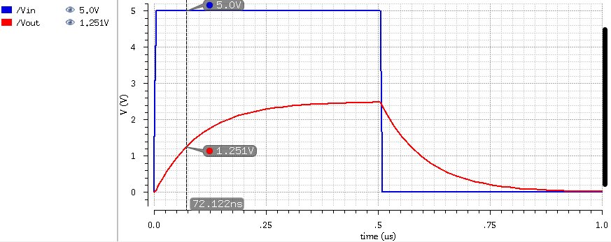
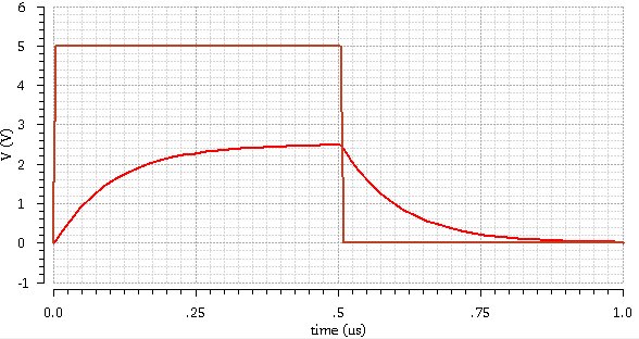
extracted view instead of the schematic. The following table shows the
simulation result comparisons between the schematic simulation and the
layout simulation.
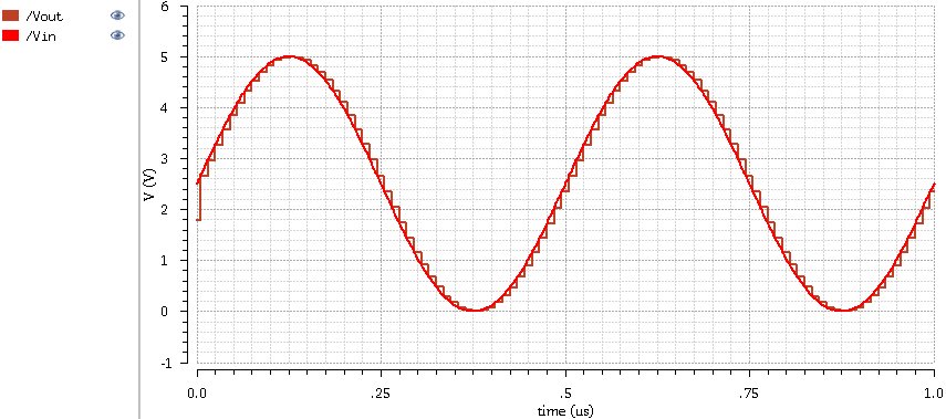
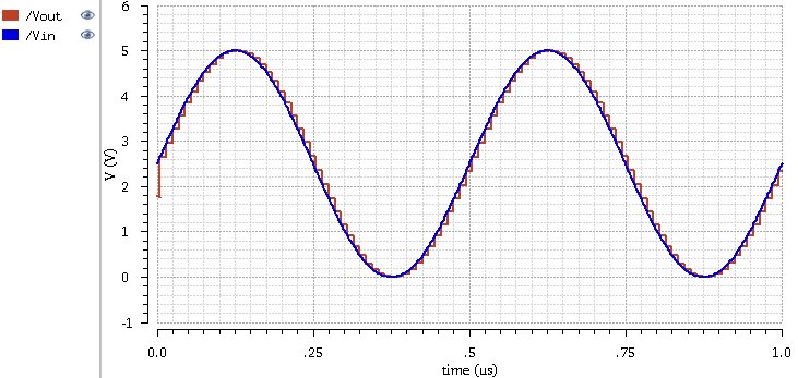
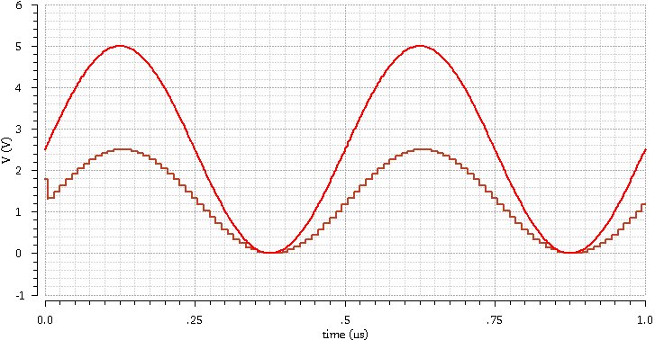
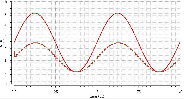
Schematic
|
Layout
|

|

|
Unit test. 0 to VDD pulse on pin B9 with all other inputs grounded. 50% delay verified.
|

|

|
ADC to DAC with no load
|

|

|
10K load
|

|

|
10p load
|
 |

|
10k and 10p load
|
Figure 7
|
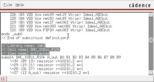
- In ADE L, going to Simulation > Netlist > Display, we can verify that the extracted view is used.

|
Figure 8
|
lab03.zip can be downloaded for verification.
All backed up work can be found at https://github.com/martinjaime/CMOSedu-Reports
EE421L Lab Student Listing | My Lab Directory | EE421 Home Page
