Project -
EE 421L
Digital Integrated Circuit Design
Generating a
test chip layout for submission to MOSIS for Fabrication
Pre-Lab Excercises
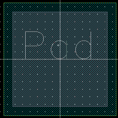
| Layout of a single
pad! |
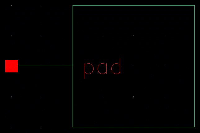
Symol of a single
pad! |
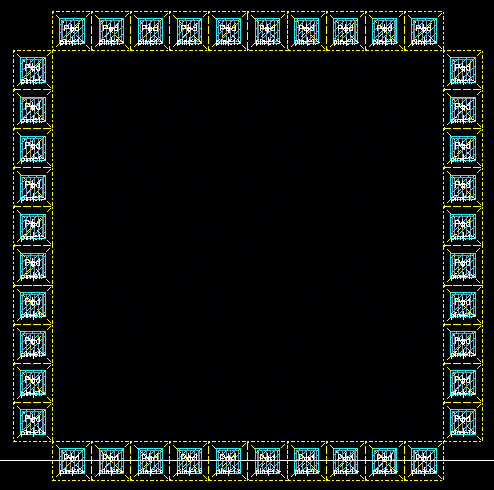
| Full layout of
complete padframe! |
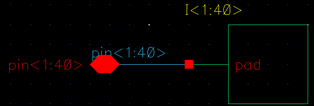
Symbol of the
complete padframe! |
Post-Lab Excercises
25K Ohm Resistor
schematic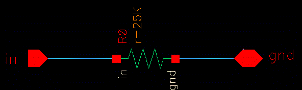 |
Symbol
used for the 25K schematic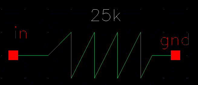 |
Simulation
Schematic using the 25k resistor symbol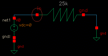 |
Simulation
of the 25k resistor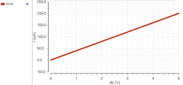 |
Layout View Extracted View 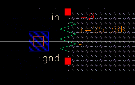 |
DRC LVS 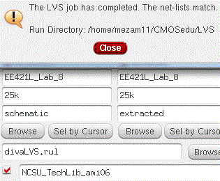 |
Attenuator Schematic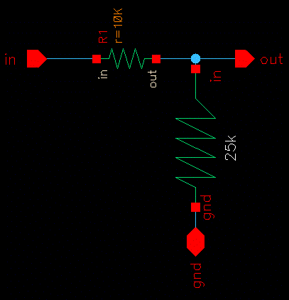 |
Symbol of Attenuator
Schematic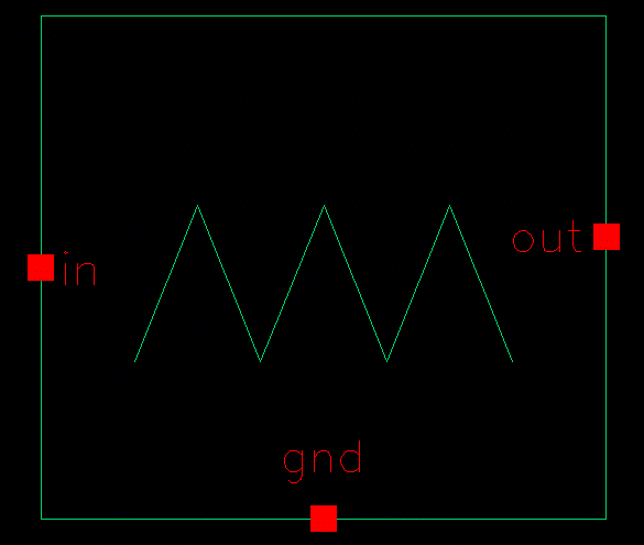 |
Simulation Schematic
for Attenuator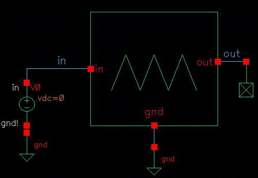 |
Simulation of the
Attenuator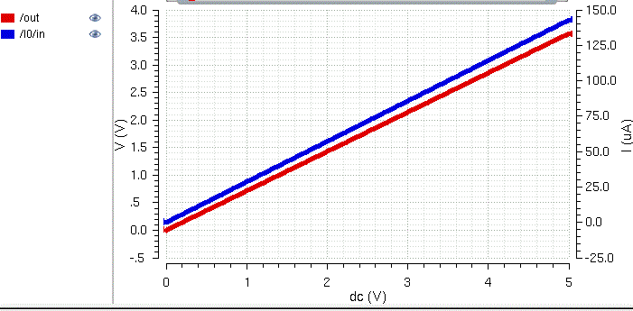 |
Layout Extracted 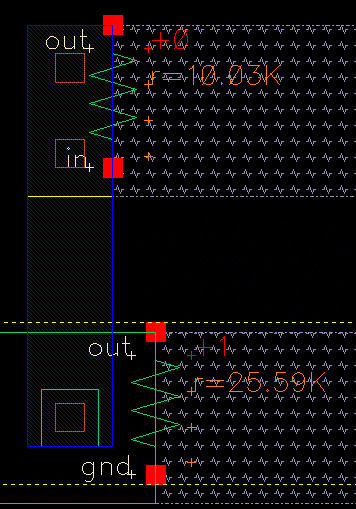 |
DRC LVS 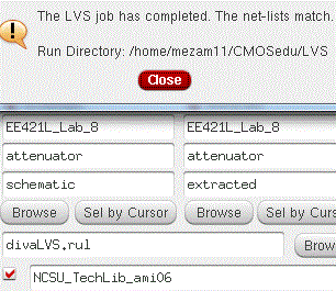 |
6u/.6u NMOS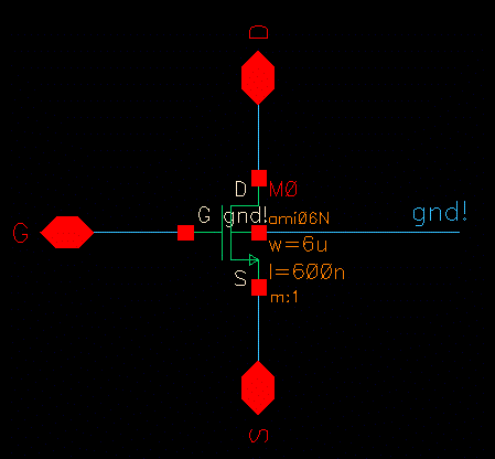 |
Symbol for the NMOS
device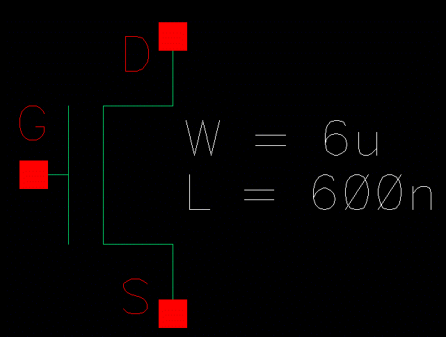 |
Simulation schematic
of the NMOS device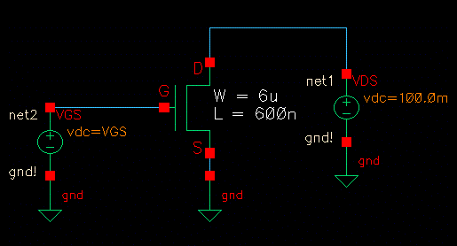 |
ID vs VDS with
incremental VGS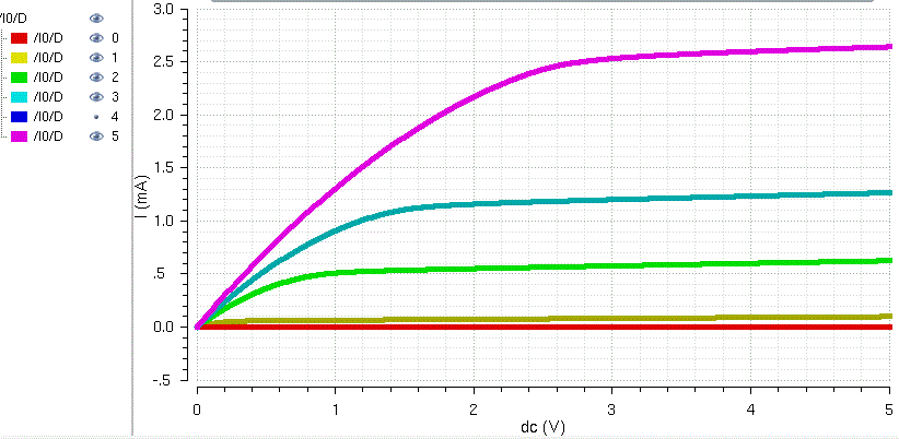 |
ID vs VGS with VDS =
0.1 Volts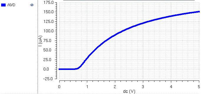 |
ID vs VGS with VDS =
5 volts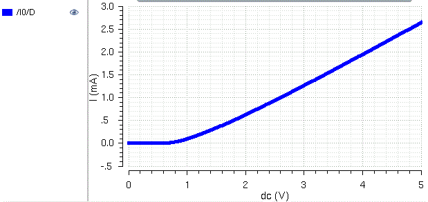 |
NMOS Layout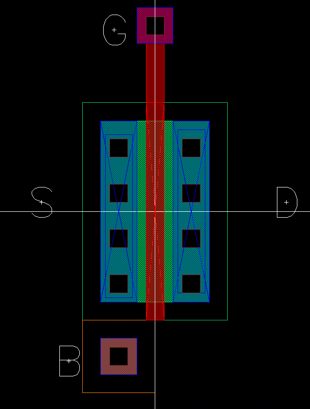 |
DRC LVS 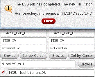 |
6u/.6u PMOS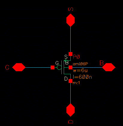 |
Symbol for PMOS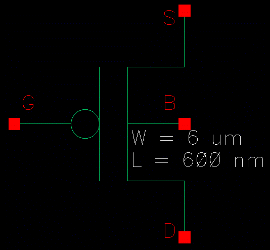 |
Simulation of PMOS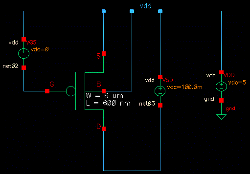 |
ID vs VSD with
incremental VSG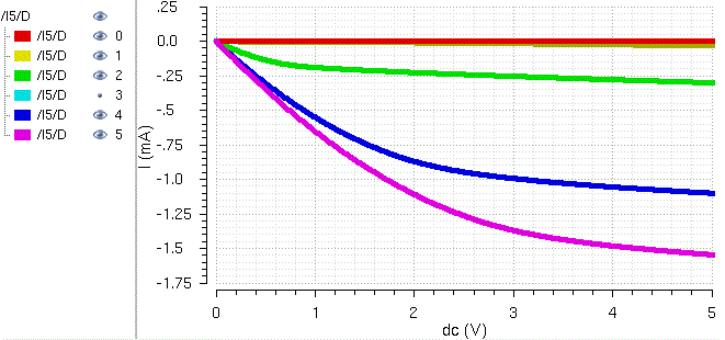 |
ID vs VSG with VSD =
0.1 volts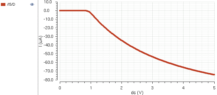 |
ID vs VSG with VSD =
5 volts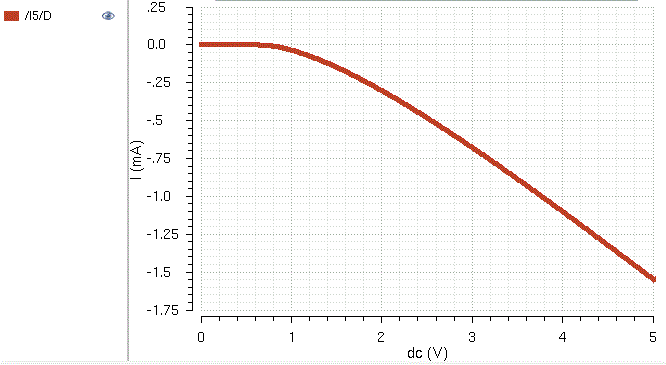 |
PMOS Layout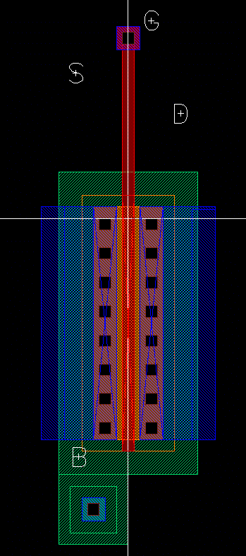 |
DRC LVS 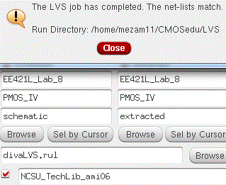 |
12u/6u Inverter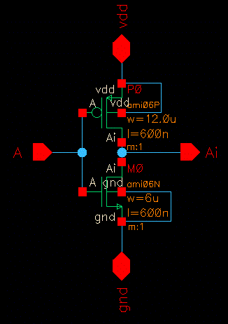 |
Inverter Symbol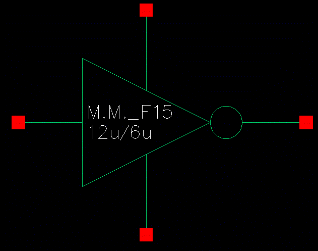 |
Simulation Schematic
of the inverter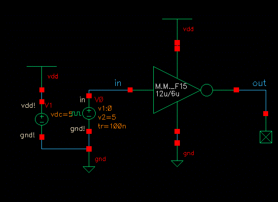 |
Simulation of the
inverter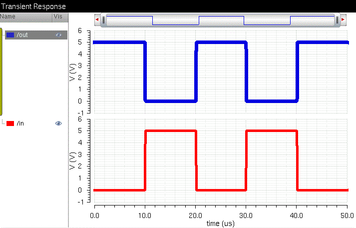 |
Inverter
Layout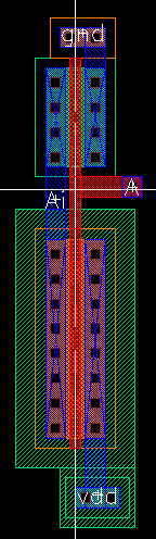 |
DRC  LVS 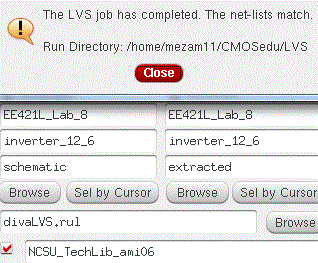 |
NAND Gate Schematic
using 6u devices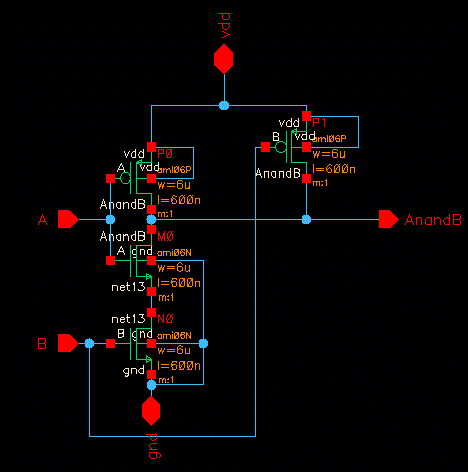 |
Symbol of the NAND
Gate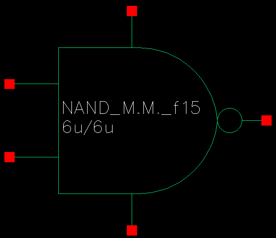 |
Simulation Schematic
of the NAND Gate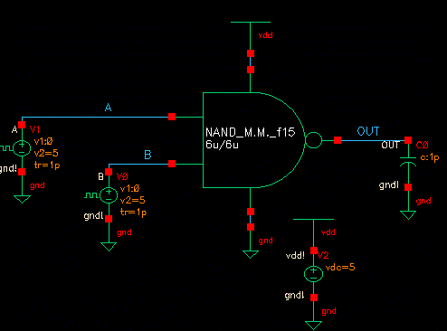 |
Simulation of the
NAND Gate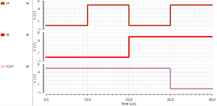 |
NAND Layout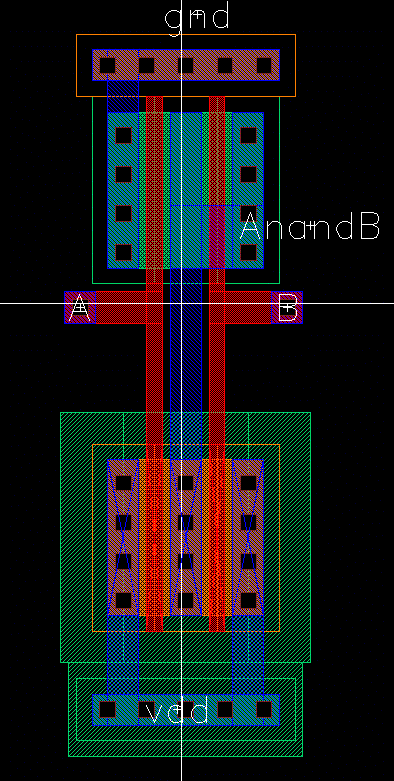 |
DRC  LVS 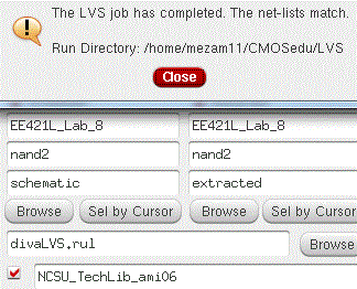 |
NOR Gate schematic
using 6u Devices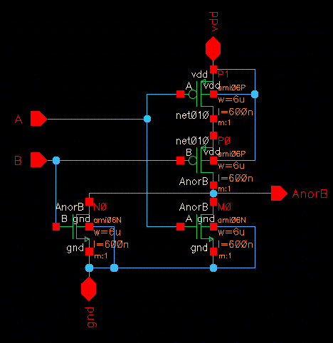 |
NOR Gate Symbol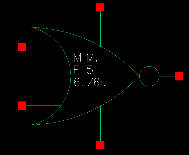 |
NOR Gate Simulation
Schematic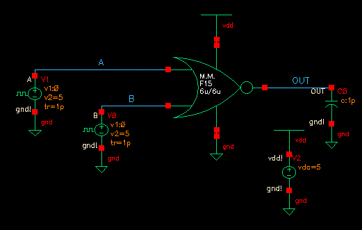 |
NOR Gate Simulation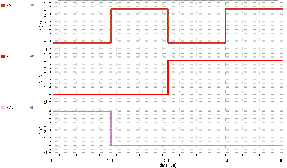 |
NOR Layout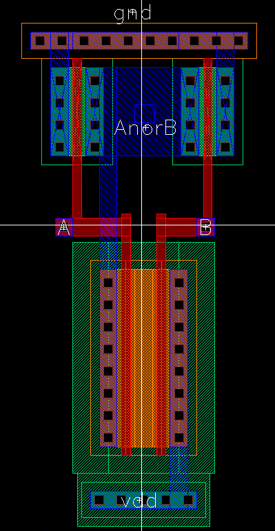 |
DRC LVS 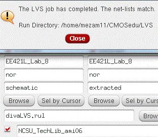 |
Ring Oscillator
Schematic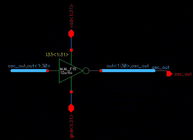 |
Ring Oscillator
Symbol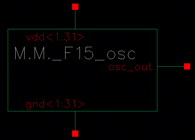 |
Buffer for Ring Osc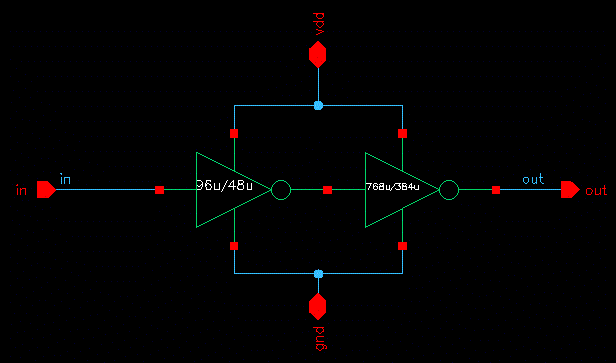 |
Buffer Symbol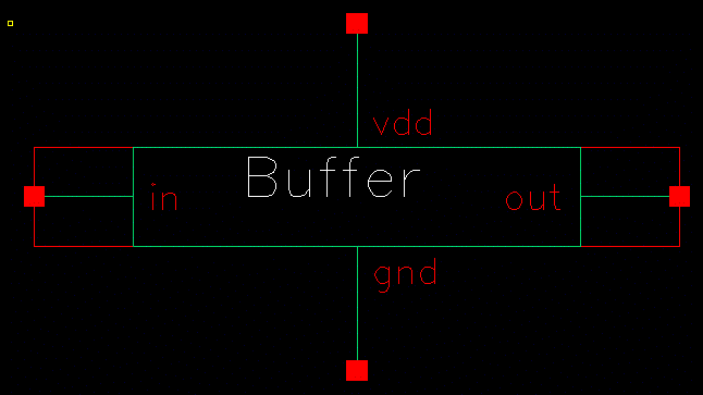 |
Ring Osc with Buffer
Schematic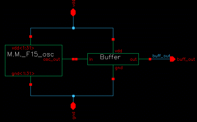 |
Ring Osc with Buffer
Symbol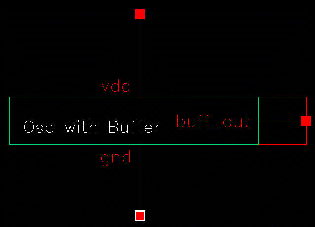 |
Simulation Schematic
of Osc with Buffer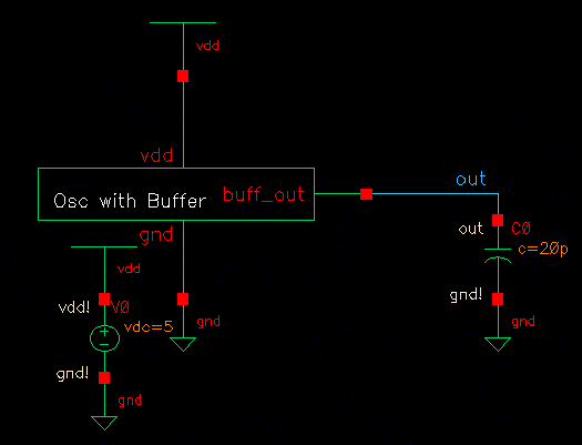 |
Simulation of the
Ring Osc/Buffer with a 20pF Load!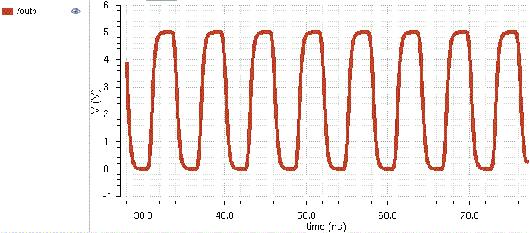 |
Buffer Layout! Notice the multiple transistors. 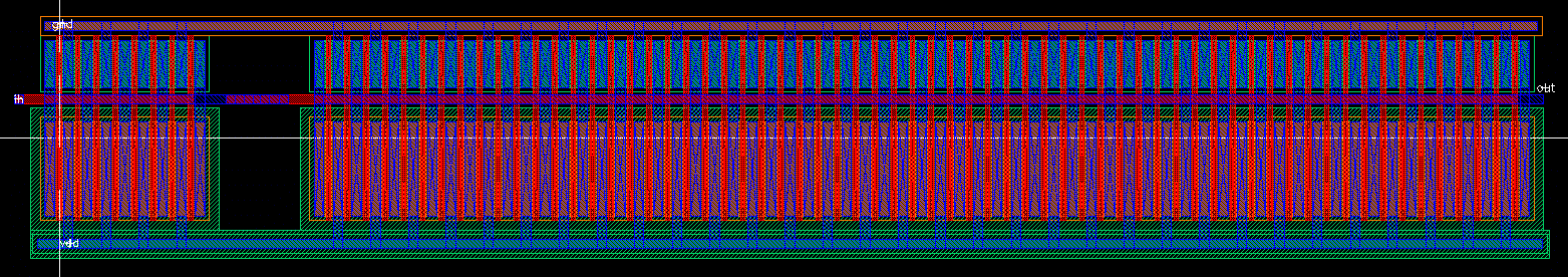 |
Buffer DRC Buffer LVS 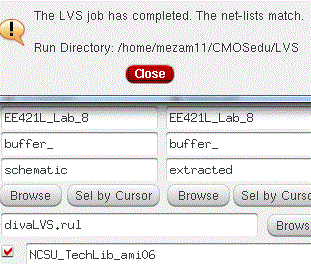 |
Ring Oscillator 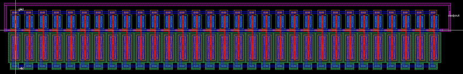 |
Ring Osc DRC Ring Osc LVS 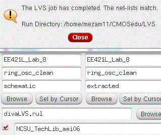 |
D - Flip Flop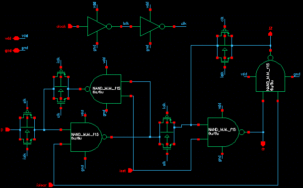 |
D - Flip Flop Symbol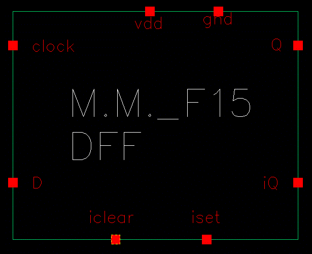 |
1-Bit Counter with enable, load input, up/down, and
clear!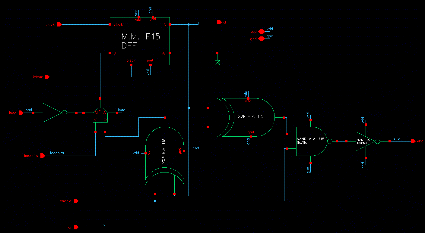 |
1-Bit Counter Symbol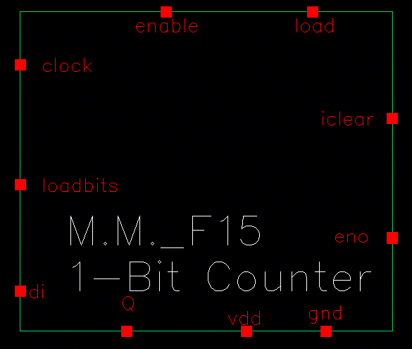 |
8-Bit Counter with enable, load, up/down, and
clear!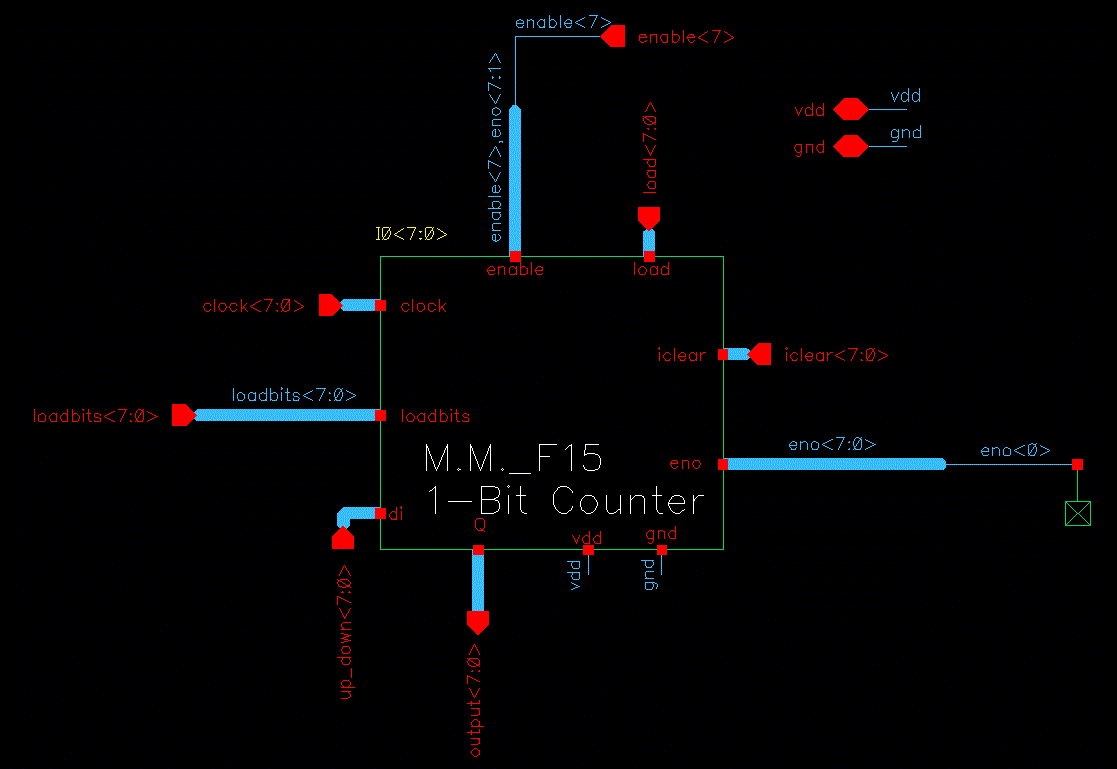 |
8-Bit Counter Symbol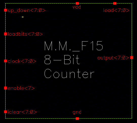 |
Layout of the DFF, Click for larger image 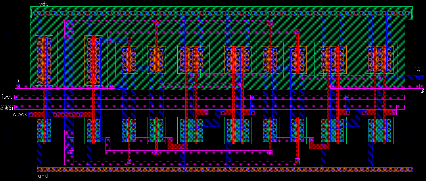 DRC and LVS will be shown later |
Layout
of the 1-Bit Counter, Click for larger image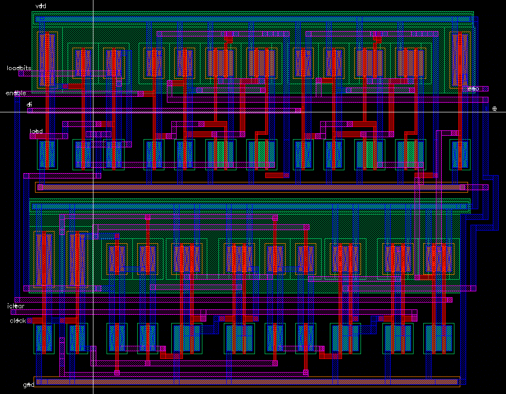 DRC and LVS will be shown later |
8-Bit Counter Simulation Schematic! Voltage Sources
were changed to include many different simulation!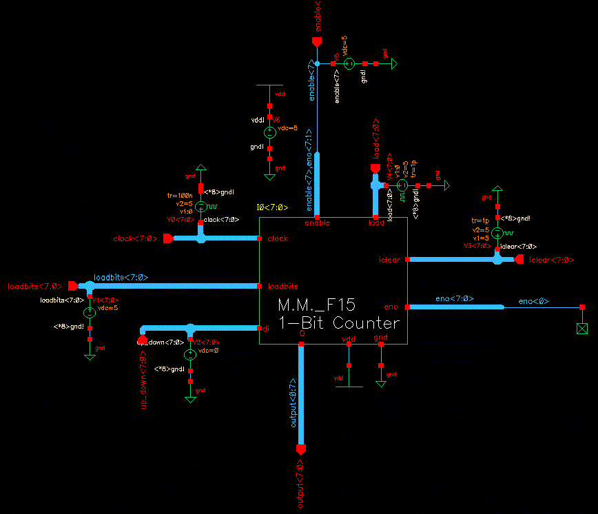 |
Counter in the count down setting!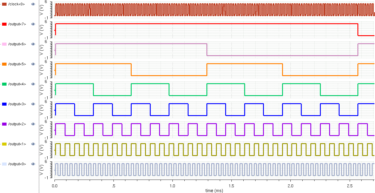 |
Counter in the up count setting!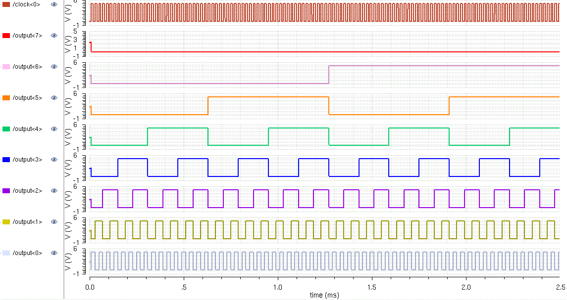 |
| Counter in the up position with "Clear" enabled at
500us! |
Counter being Loaded in with the following bit value:
11111111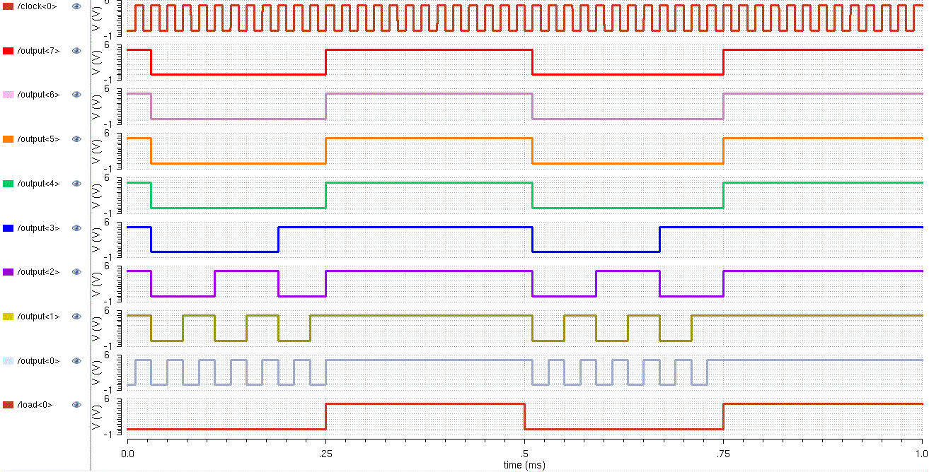 |
| Counter in the up position demonstrating the Reset
(Clear) function! |
Layout of the 8-Bit Counter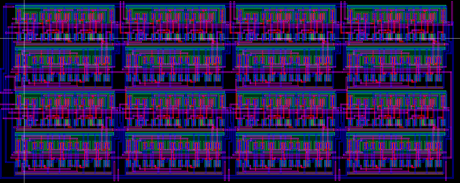 |
LVS and DRC of the 8-Bit Counter 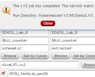 |