Lab 4 - ECE 421L
See the EE421L webpage here
Authored by Juan Buendia
buendiaj@unlv.nevada.edu
September 28, 2015
Objective: Charactersistics and layout of NMOS and PMOSdevices in ON's C5 Process
Pre-lab work
- Back-up all of your work from the lab and the course.
- Read through this lab before starting it.
- Go through Tutorial 2 seen here.
- In
the simulations in this lab the body of all NMOS devices (the
substrate) should be at ground (gnd!) and the body of all PMOS devices
(the n-well) should be at a vdd! of 5V.
Tutorial 2 will have us create a symbol, schematic, layout, and a simulation schematic of NMOS, and a PMOS Device.
Nmos Device
Schematic
Symbol
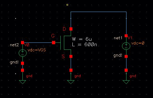
Use
a simulation schematic to perform a simulation. We will sweep Vds
from 0 - 5 V in 1mV steps for VGS = 1V, 2V, 3V, 4V, and 5V.
Simulation
Schematic
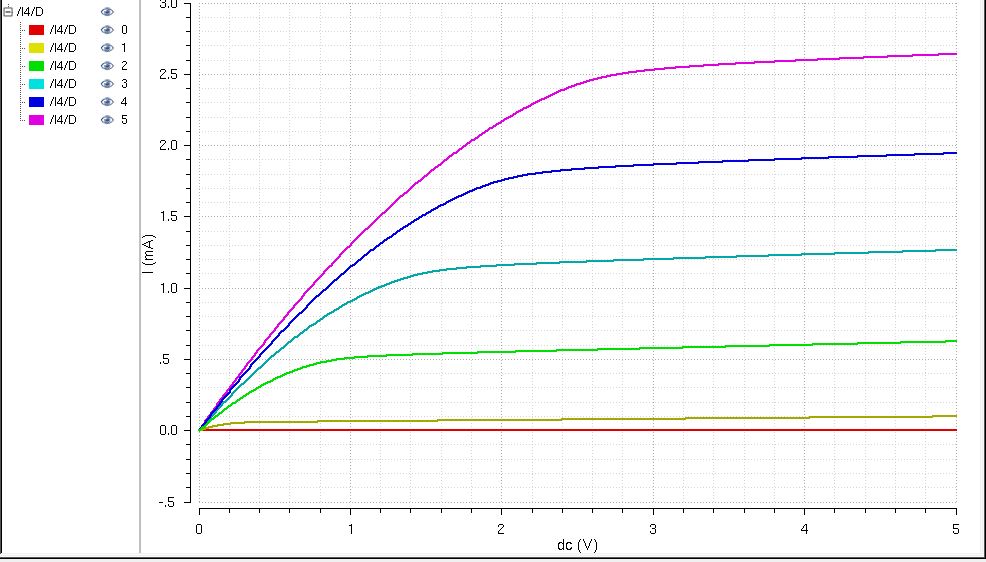
Simulation Results
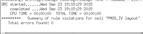
Create a Layout of the NMOS Device, extract it, check for design rules, and perform an LVS
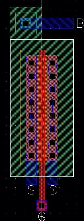
Layout
Extracted
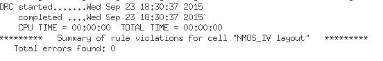
DRC
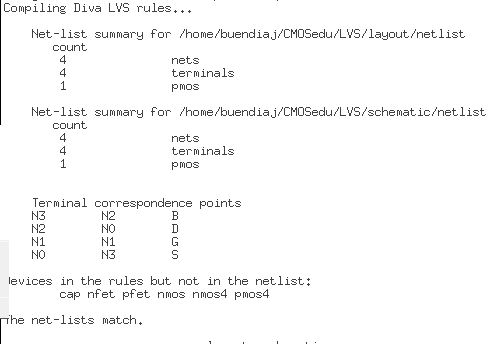
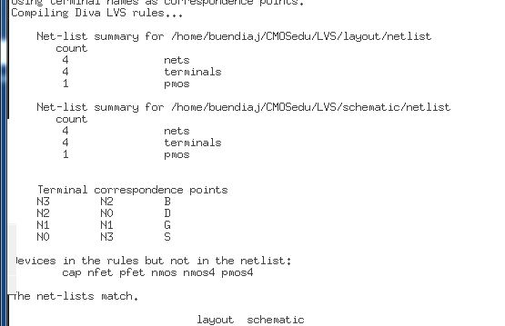
LVS
Extracted Simulation
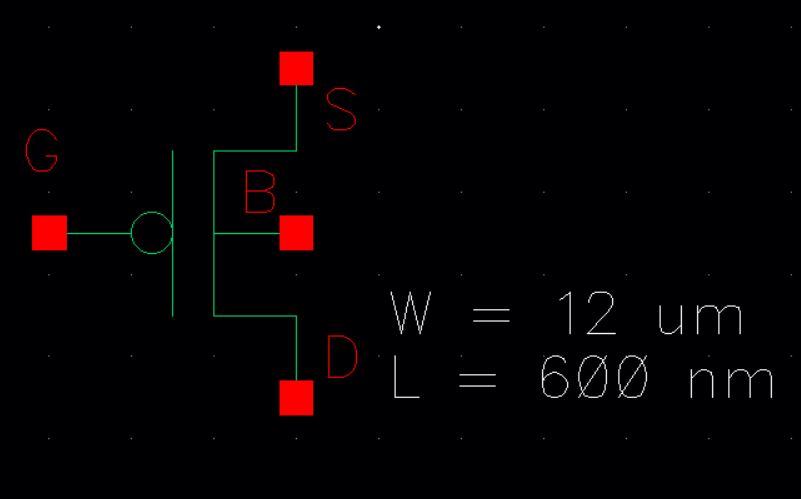
Pmos Device
Schematic
Symbol
Use
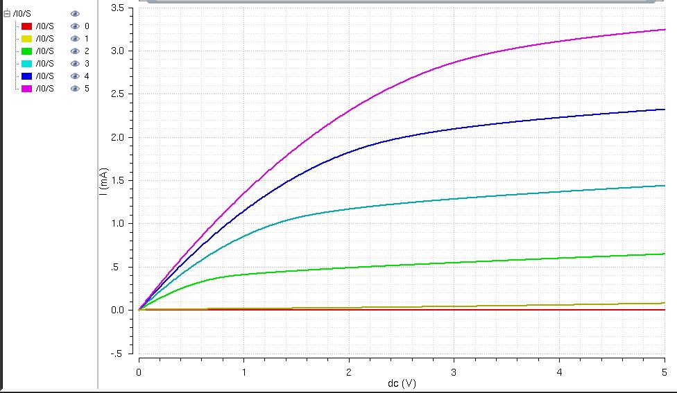
a simulation schematic to perform a simulation. We will sweep Vsd from
0 - 5 V in 1mV steps for Vsg = 1V, 2V, 3V, 4V, and 5V.
Simulation
Schematic
Simulation Results
Create
a Layout of the PMOS Device, extract it, check for design rules, and perform an
LVS.
Layout
Extracted
DRC
LVS
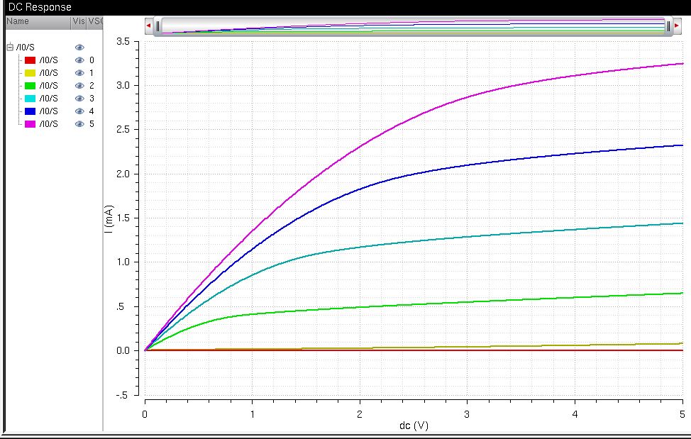
Extracted Simulation
Post Lab
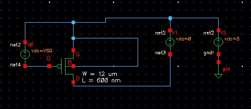
- Generate 4 schematics and simulations (see the examples in the Ch6_IC61 library, but note that for the PMOS body should be at vdd! instead of gnd!):
- A schematic for simulating
ID v. VDS of an NMOS device for VGS varying from 0 to 5 V in 1 V steps
while VDS varies from 0 to 5 V in 1 mV steps. Use a 6u/600n
width-to-length ratio.
- A
schematic for simulating ID v. VGS of an NMOS device for VDS = 100 mV
where VGS varies from 0 to 2 V in 1 mV steps. Again use a 6u/600n
width-to-length ratio.
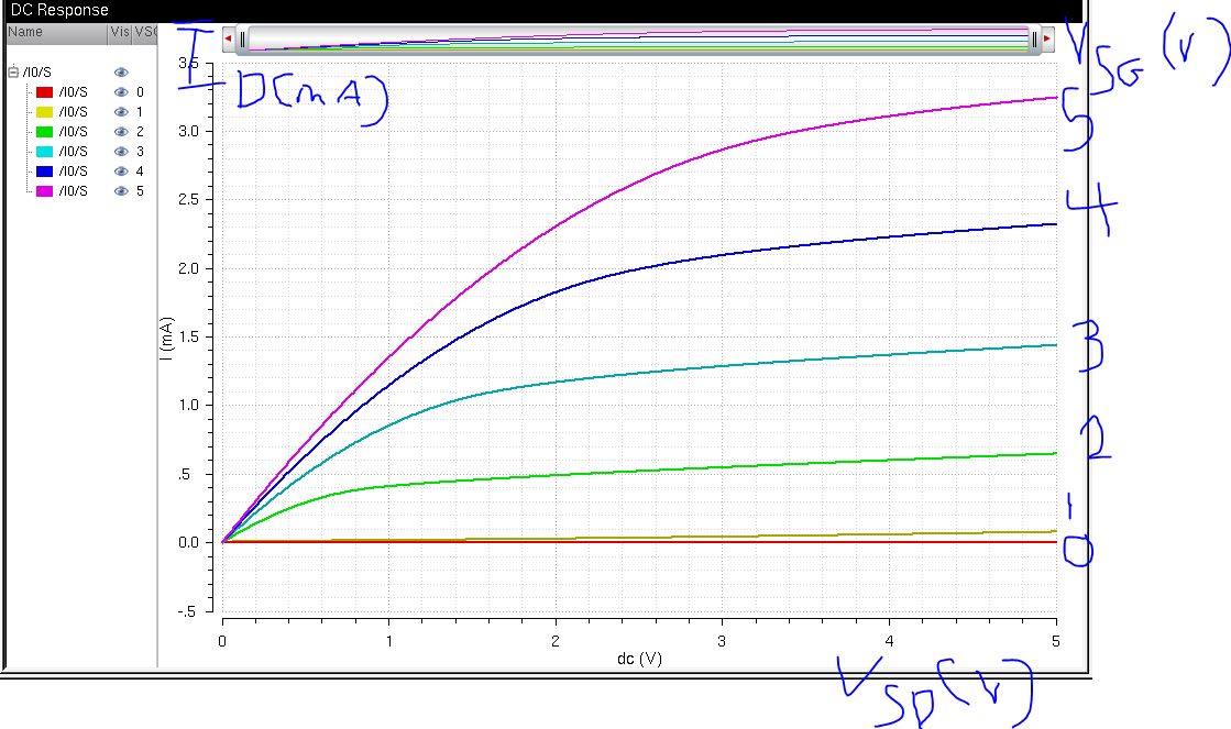
- A
schematic for simulating ID v. VSD (note VSD not VDS) of a PMOS device
for VSG (not VGS) varying from 0 to 5 V in 1 V steps while VSD varies
from 0 to 5 V in 1 mV steps. Use a 12u/600n width-to-length ratio.
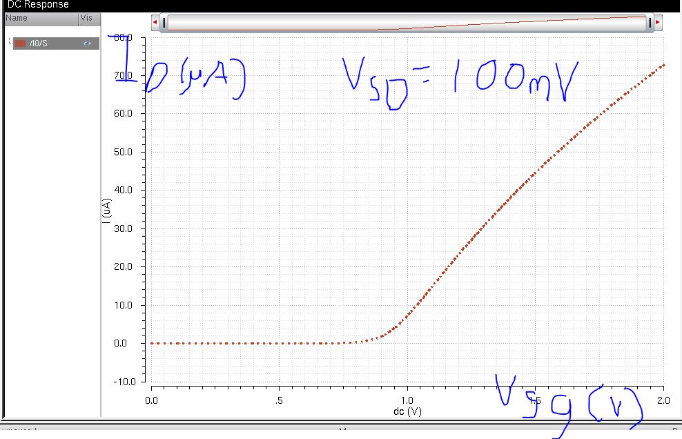
- A
schematic for simulating ID v. VSG of a PMOS device for VSD = 100 mV
where VSG varies from 0 to 2 V in 1 mV steps. Again, use a 12u/600n
width-to-length ratio.
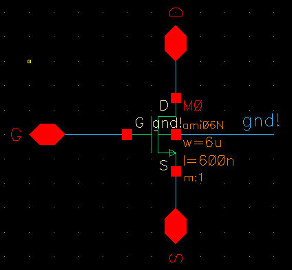
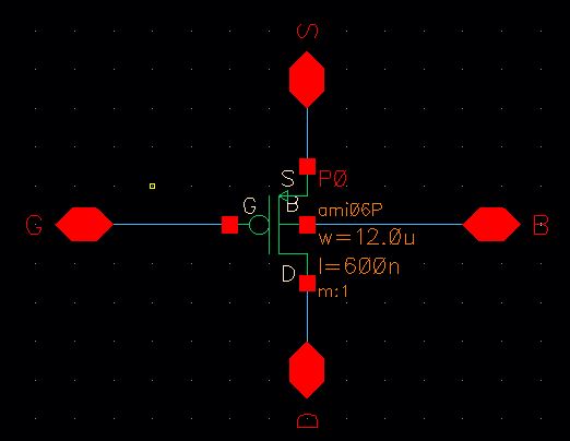
The Schematics are based on the same NMOS and PMOS schematics for the prelab
Nmos
Pmos
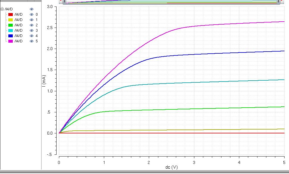
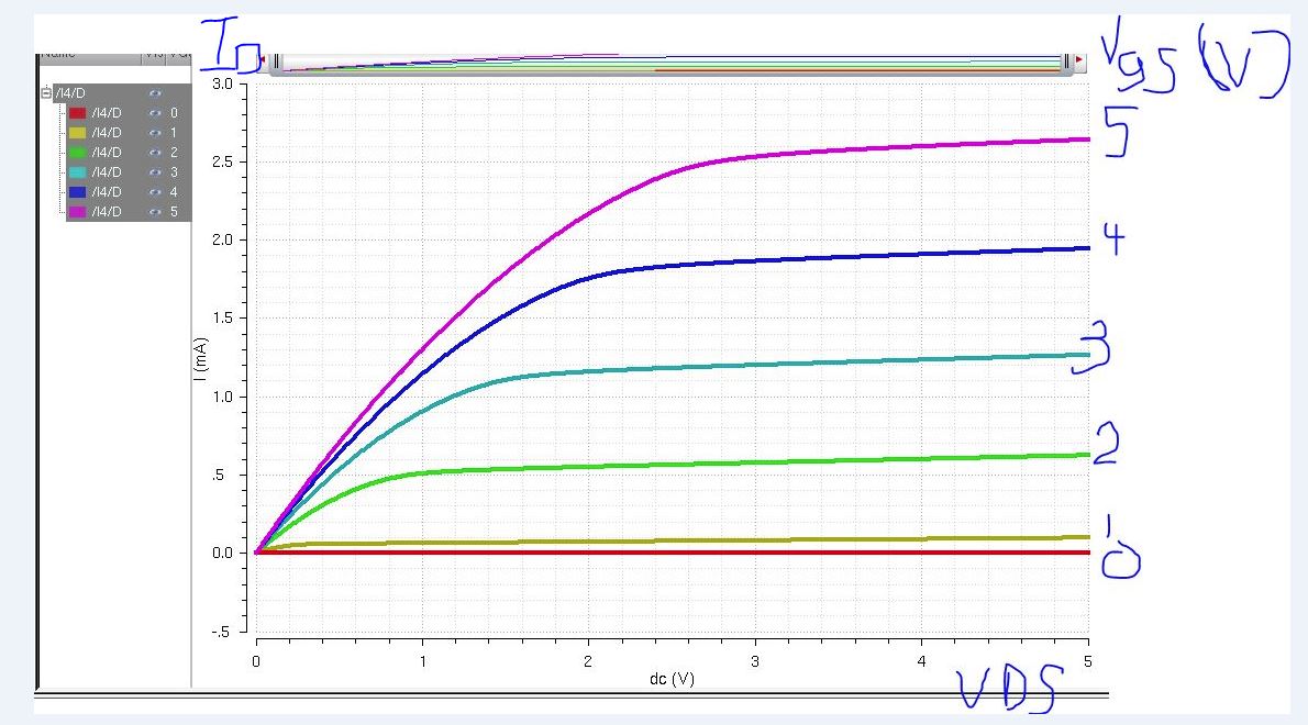
NMOS Simulation - ID versus VGS stepping from 0 - 5 in 1 V steps,and VDS stepping from 0 - 5 V in 1mV steps.
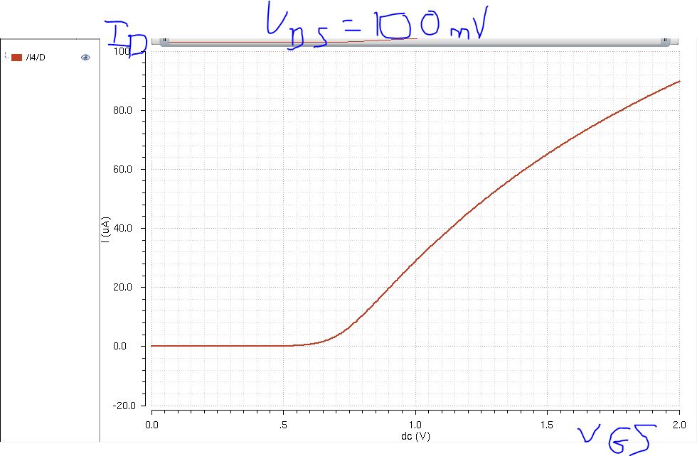
Nmos Simulation - Id versus VDS - 100mV and VGS stepping from 0 - 2mV in 1mV steps
Pmos Simulation - Id versus VSG stepping from 0 - 5V in 1 V steps and VSD sweeps from 0 - 5V in 1mV steps
PMOS simulation - Id versus VSD = 100mV and VSG stepping from 0 - 2V in 1mV steps.
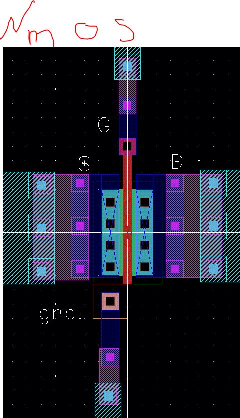
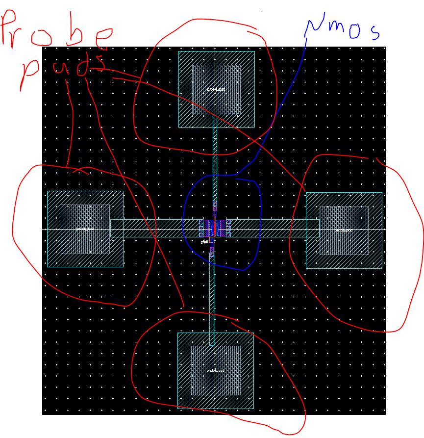
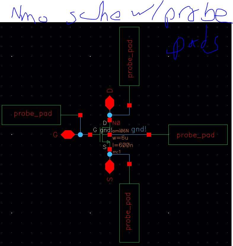
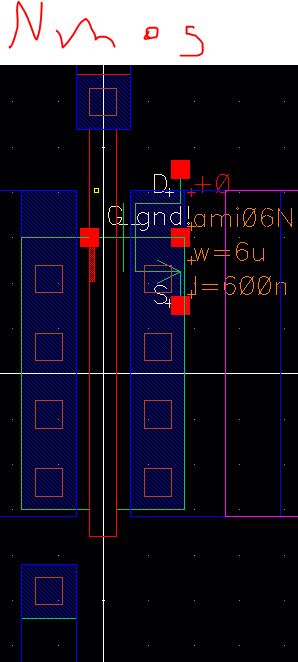
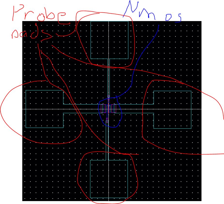
- Lay
out a 6u/0.6u NMOS device and connect all 4 MOSFET terminals to probe
pads (which can be considerably smaller than bond pads [see MOSIS design rules] and directly adjacent to the MOSFET (so the layout is relative small).
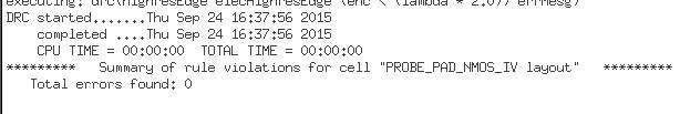
- Show your layout passes DRCs.
- Make a corresponding schematic so you can LVS your layout.
Layout
Zoomed In
Layout Showing probe Pads
LVS Schematic
Extracted
Zoomed in
Extracted Zoomed Showing Probe Pads
DRC
LVS
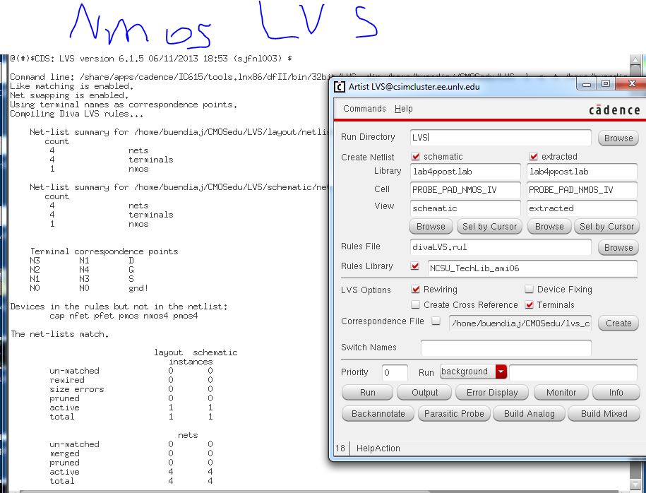
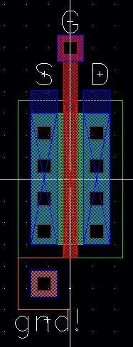
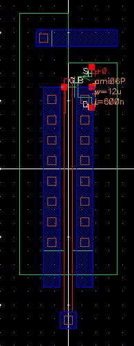
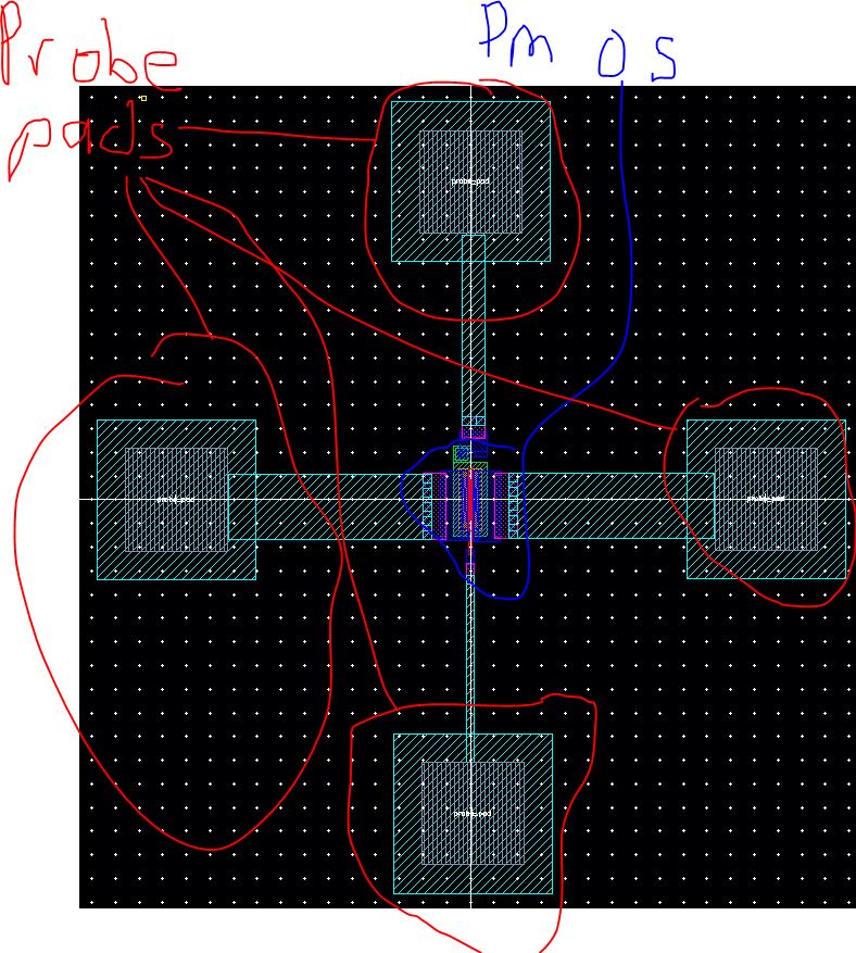
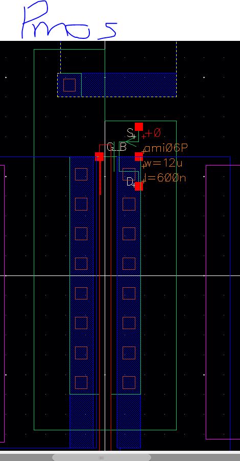
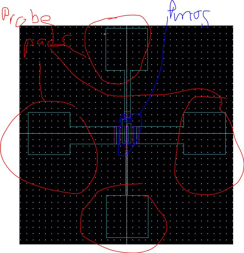
- Lay out a 12u/0.6u PMOS device and connect all 4 MOSFET terminals to probe pads.
- Show your layout passes DRCs.
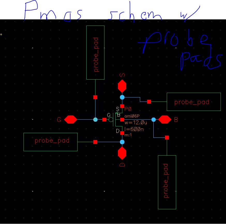
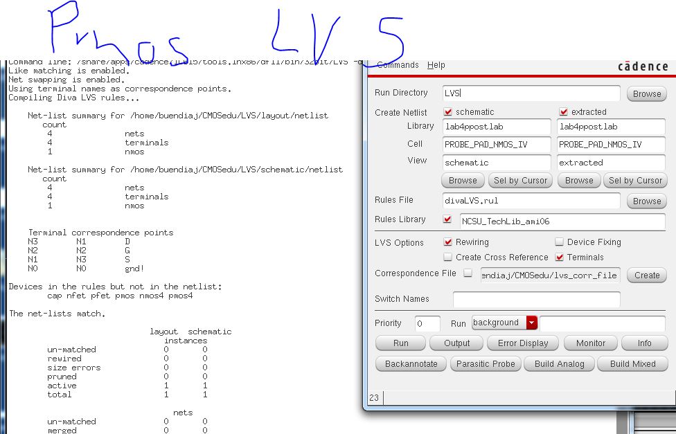
- Make a corresponding schematic so you can LVS your layout.
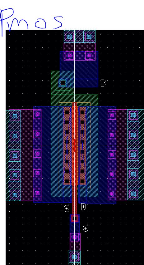
Layout
Zoomed In
Layout Showing probe Pads
LVS Schematic
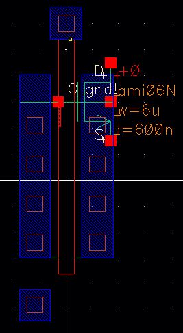
Extracted
Zoomed in
Extracted Zoomed Showing Probe Pads
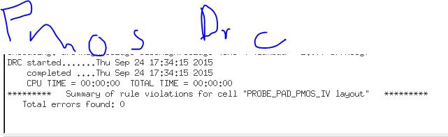
DRC
The final step is to back up the lab 4 file
Return to buendiaj's labs
Return to EE421L Labs