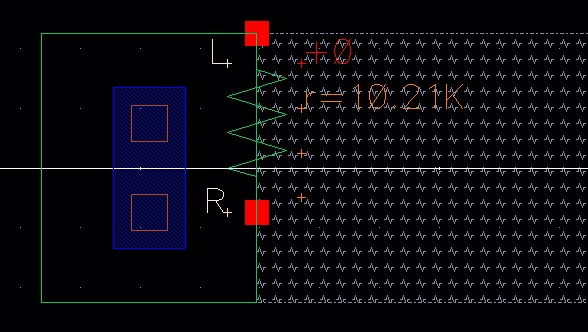
The extracted view shows that the resistor is valued at around 10k:
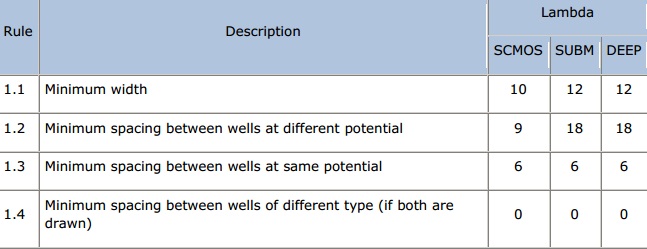
The rules from MOSIS for a n-well are seen below:
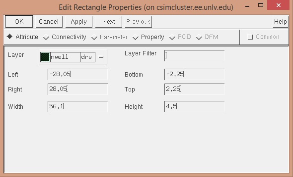
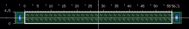
Keeping the minimum widths in mind, we pick L = 56.1 and W = 4.5. To calculate the 10k we have R = (56.1 / 4.5) * 800 Ohms/Square ~ 10k:
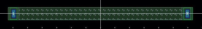
To measure the values in the layout, we use Rulers which can be accessed by the hotkey K. Seen below, the widths match up with what they should be:
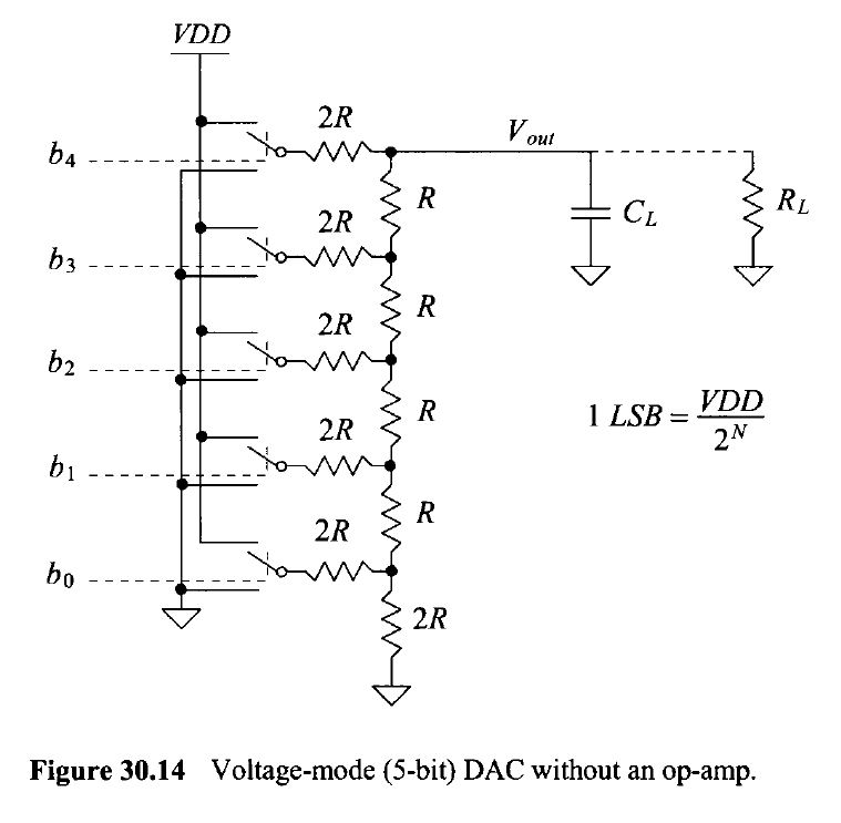
Below is a circuit for a 5-bit DAC which we will be basing our design on:
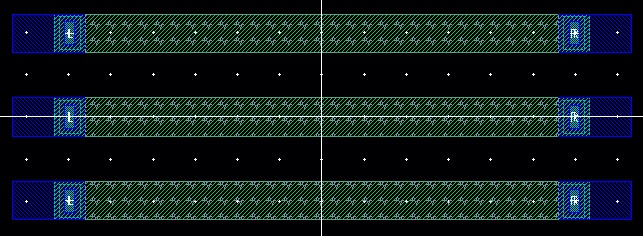
We begin by laying out three 10k resistors and adding metal1 to the ends:
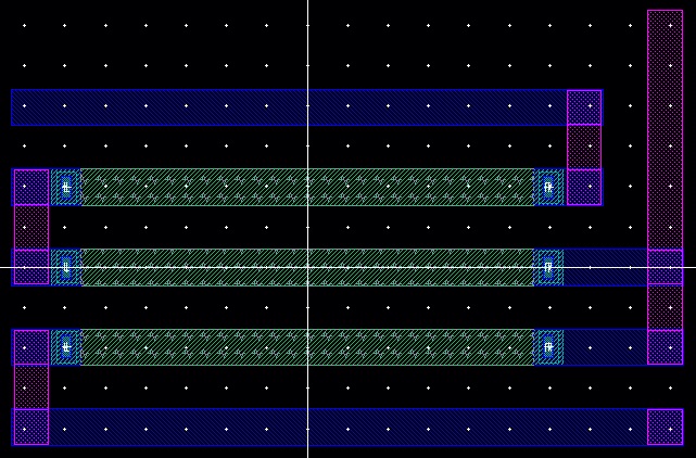
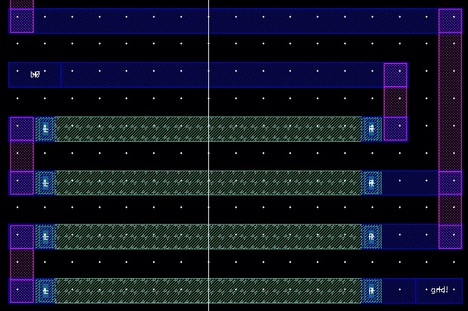
Next we place Vias by using the component m1_m2. We next place layers of metal2 in order to properly connect the resistors and pins. Below you will see a template for 1-bit of the DAC that we can repeat 10 times:
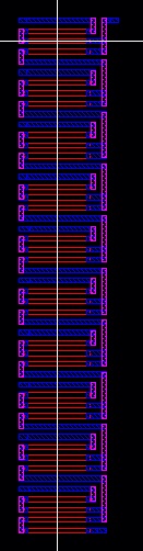
We connect all 10 of the bits together, and assign pins as seen in the final layout below:
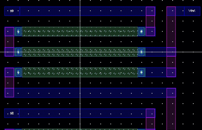
Seen below, the first and last bit have slightly different layouts to account for Vout and GND:
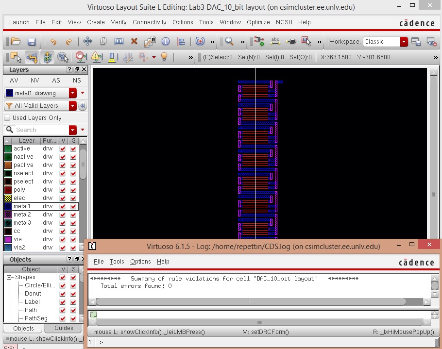
To complete the lab, we do a DRC to make sure no rules are broken:
The lab is now complete, and it is time to backup our work. This task is completed in the exact same way that it is seen in Lab 1.
The complete project can be found at the following link lab3.zip