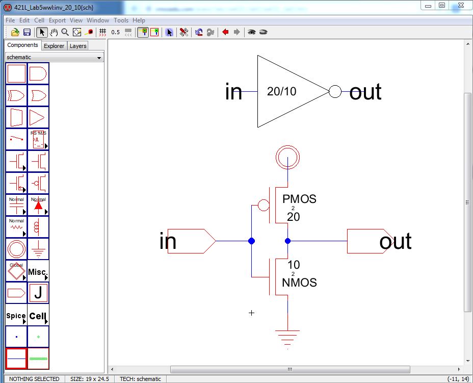
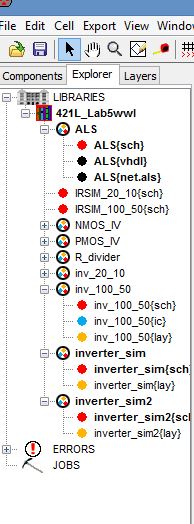
Lab 5 - ECE 421L
2.
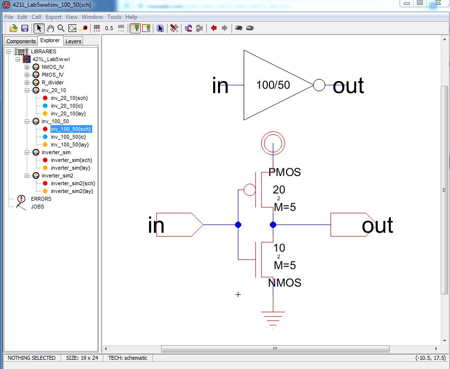
Second, follow the inverter design procedure and make a another one
with W=100, L=50. Learn how to use the "Add Multiplier" command to
design 5 MOSFET in parallel to get 100/2 PMOS and 50/2 NMOS.
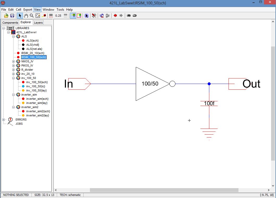
Duplicate the "inv_20_10" cell to "inv_100_50" cell. Click the new cell and select the PMOS. Then press tools --> Simulation (spice) --> add Multiplier to set the M=5 adding 5 parallel PMOS. Do the same to NMOS. Others are kept the same as before. We can get the following circuit.
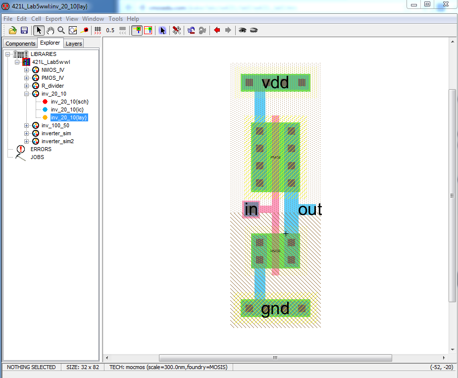
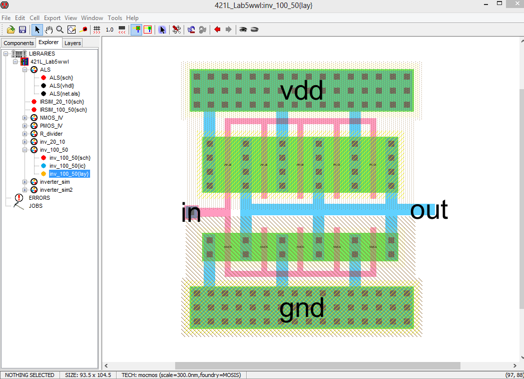
3. Then, lay out the 100/50 inverter. Put 5 PMOSs on the same Y axis and put 5 NMOSs on the downside same Y axis. Then connect all the poly together and name the export "In". Then connect drain of PMOSs and NMOSs together to the export "Out". After that, connect PMOS source to up vdd and NMOS to down gnd. So the inverter has 4 terminals: In, Out, vdd, gnd. Make sure the layout passes the DRC, ERC, NCC.
Simulations
1. SPICE simulation using three different load capacitors: 100fF, 1pF, 10pF.
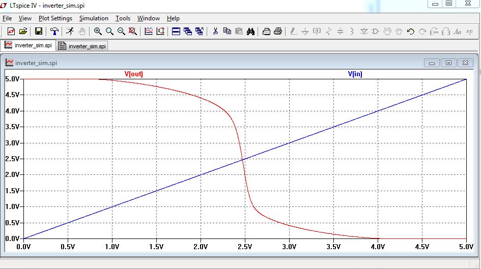
First, simulate the 20/10 inverter giving a pulse input. And see the output signal by using different load capacitors. Write down the spice code like the following,

The Simulation result is shown in below.
CL=100fF
CL=1pF
CL=10pF
Therefore, we can know that the load capacitor affects the output rise-time and fall-time.
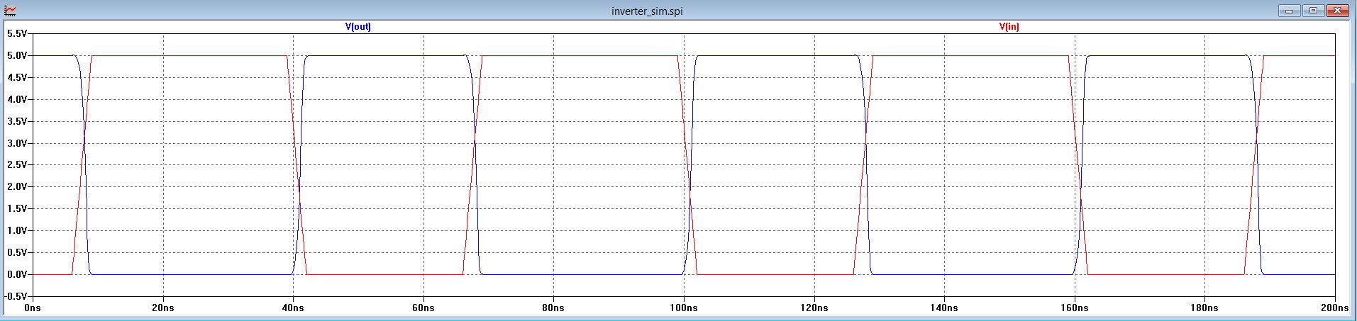
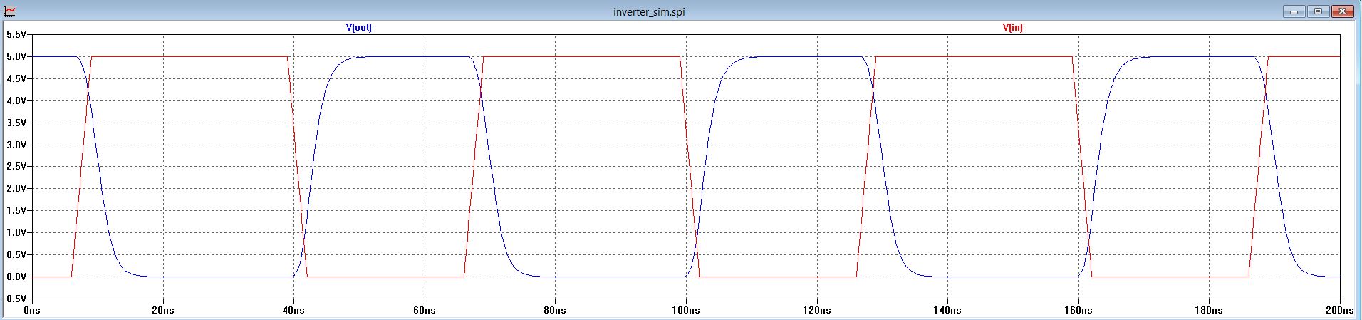
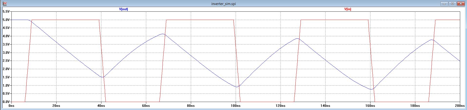
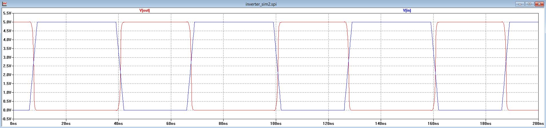
Now, we simulate the 100/50 inverter. Give the same input signal to the circuit and add three different capacitors to check the result.

The simulation is shown in below.
CL=100fF
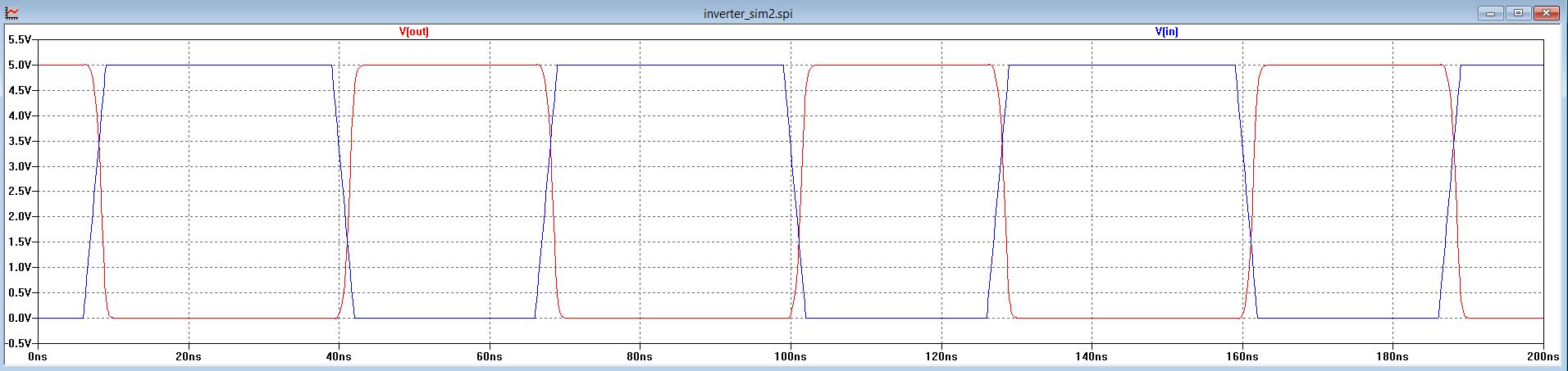
CL=1pF

CL=10pF
From the simulation result, we can understand why the large size inverter could support larger load. The result signal is still kept at a good condition.
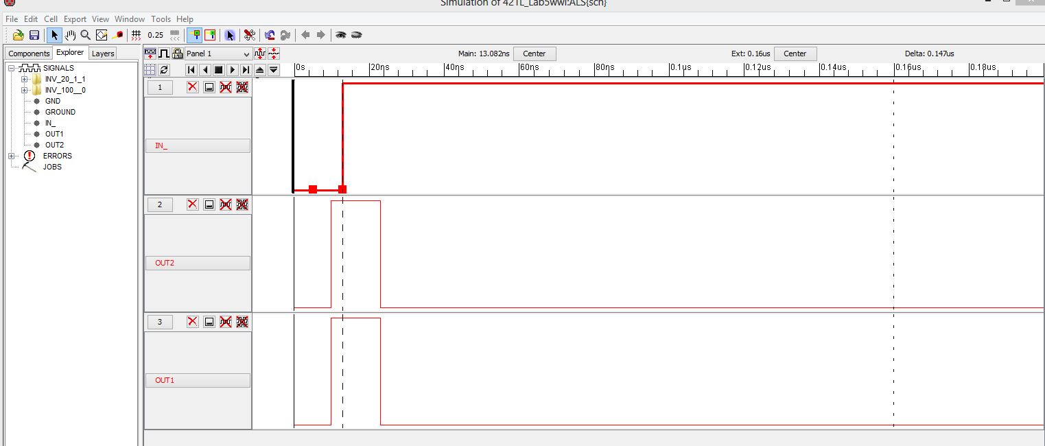
2. ALS simulation using three different load capacitors: 100fF, 1pF, 10pF.
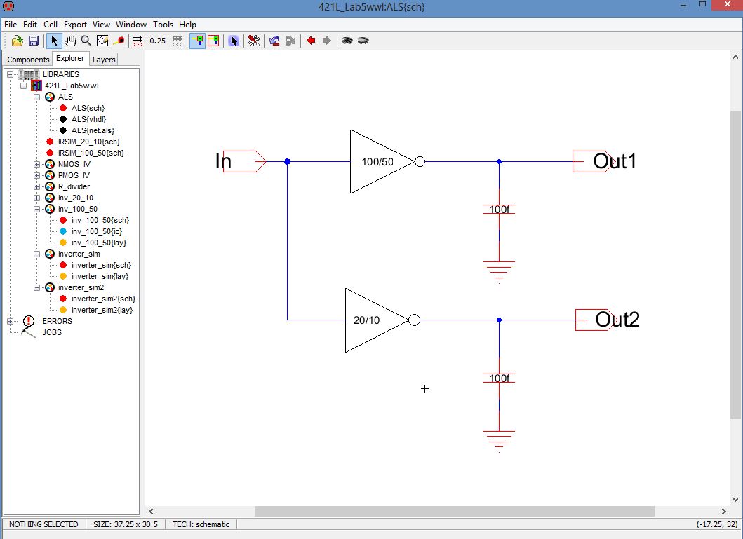
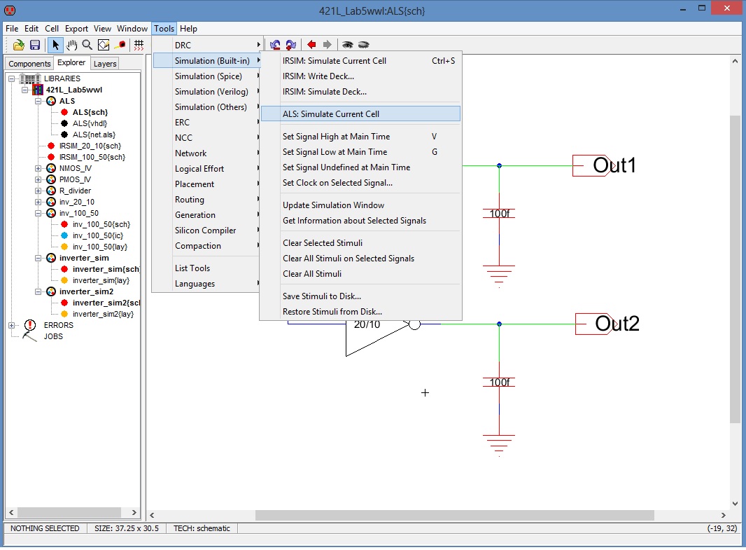
First, open a new schematic cell named "ALS". Put two inverter in it and set the export input and output. Then press tools--> Simulation (build-in) --> ALS: simulate the current cell. Then the simulation window pops up. And in the Explorer, the vhdl and net.als cells are added automatically. Set the input signal by pressing G or V to set low signal or high signal. Then we can get the immediate result of other signals: out1, out2.
The input setting is shown in below. And this is the result with 100fF load capacitor. It seems the two outputs rise and fall at the same time. They seem to have the same delay time.

The following shows the result with 1pF and 10pF load capacitor. Also, we can see these two inverters have same delay time. And the problem is that no matter how much load capacitor is, the delay time of the inveter is the same. That means ALS can only simulate to make sure whether the circuit logic is working well or not.
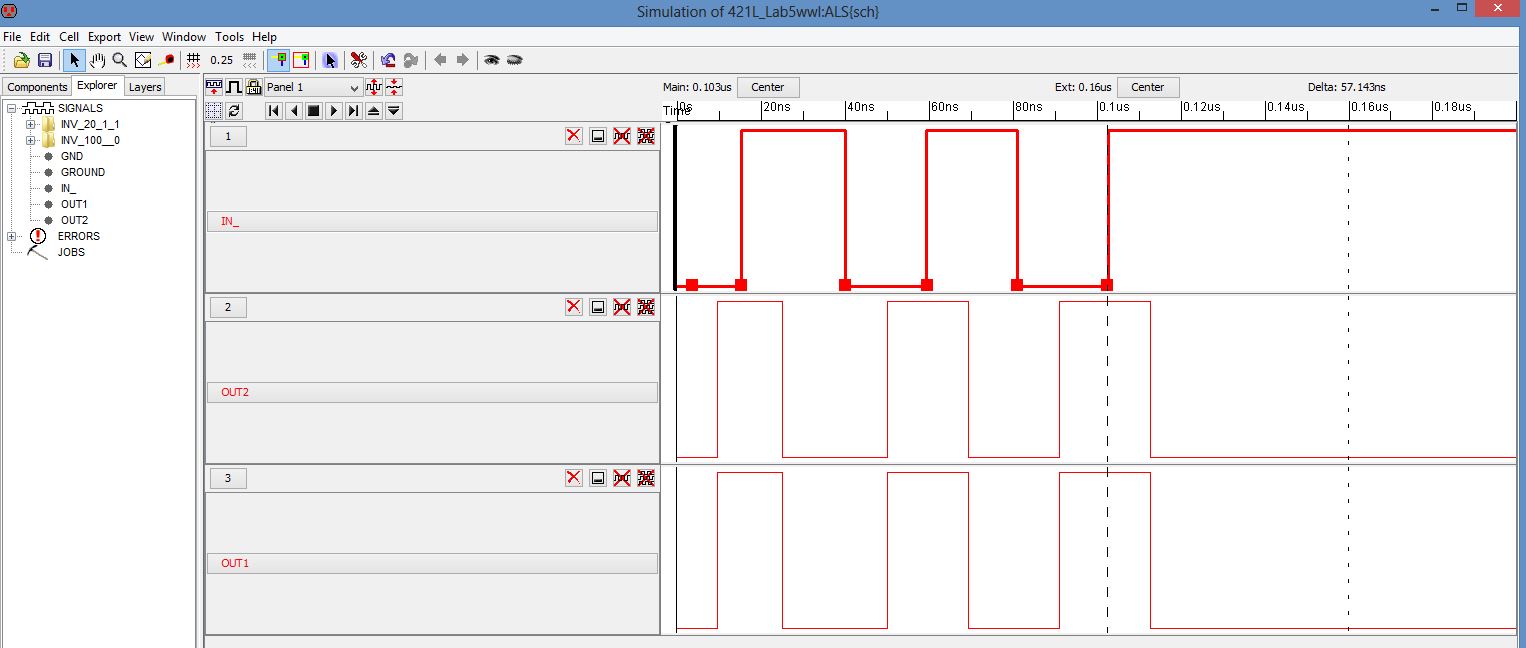
CL=1pF
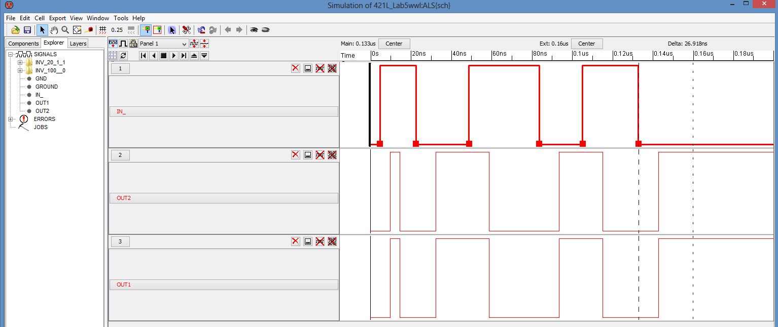
CL=10pF
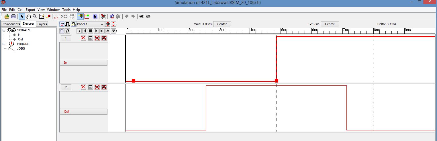
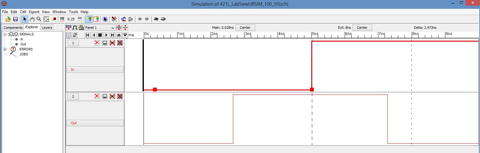
3. IRSIM simulation using three different load capacitors: 100fF, 1pF, 10pF.
Simulation using IRSIM also needs to open a new schematic cell. I open two cells: one for 20/10 inverter and the other for 100/50. Put these two icons into the respective cell.

Go tools--> Simulation (build-in) --> IRSIM: simulate the current cell. And then like ALS simulation to set up the input signal. After getting the result, set the load capacitor. The following shows the result.
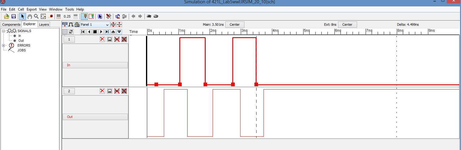

The left image is the 20/10 inverter with 100fF; the right one is 100/50 inverter with 100fF
The left image is the 20/10 inverter with 1pF; the right one is 100/50 inverter with 1pF


The left image is the 20/10 inverter with 10pF; the right one is 100/50 inverter with 10pF
From the simulation, we can totall see that the IRSIM simulation can help us to simulate the transistor level model. That is because different load capacitors have different delay time from the above simulation results.
Backup the work directory for future study
