Lab 4 - ECE 421L
2.) However, tutorial_2 uses the 4 terminals of MOSFETs as seen below. And the size of MOSFETs are all W=10, L=2.


4.) Next, design the layouts for these schematics. First, for NMOS layout, select nMOS, nACT, p-well, and Metal1_to_poly1 and put them in the layout cell. The nAct to provide a connection for metal1 Arcs to MOSFET S/D. The Meal1_to_poly1 is used for connecting metal1 to the gate terminal. P-well is to connect the substrate to ground. Second, we need to change the nMos Node's width to 10 and the x-size of nACT and p-well to 10. Then, select nMos Node, go to tools-->Simulation(Spice)-->Set Spice Model... and set the SPICE model name to NMOS(if you don't set we can't simulate the layout.)
Change x-position of the nMos Node and two nACTs making they align. Use the left mouse select the top port on the nMos Node and right mouse click the nACT. An N-Active was added between the nodes.
The p-well should be put close to S/D node. Next, left click the poly and right click the Metal1_to_poly1 to connect them. We can get the below layout. This is an NMOS layout.
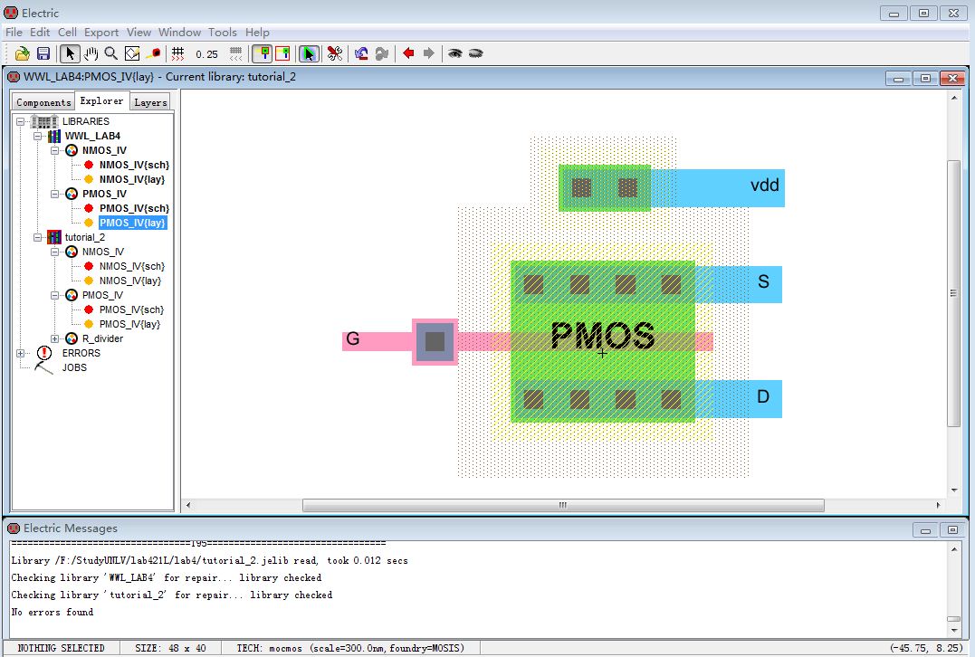
For PMOS the process is almost the same. Take care that the width is 20 instead of 10. And pMOS, pACT, n-well and Metal1_to_poly1 will be used. The n-well should be connected to vdd. The metal1 node connected to n-well should be named lowercase "vdd".
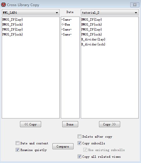
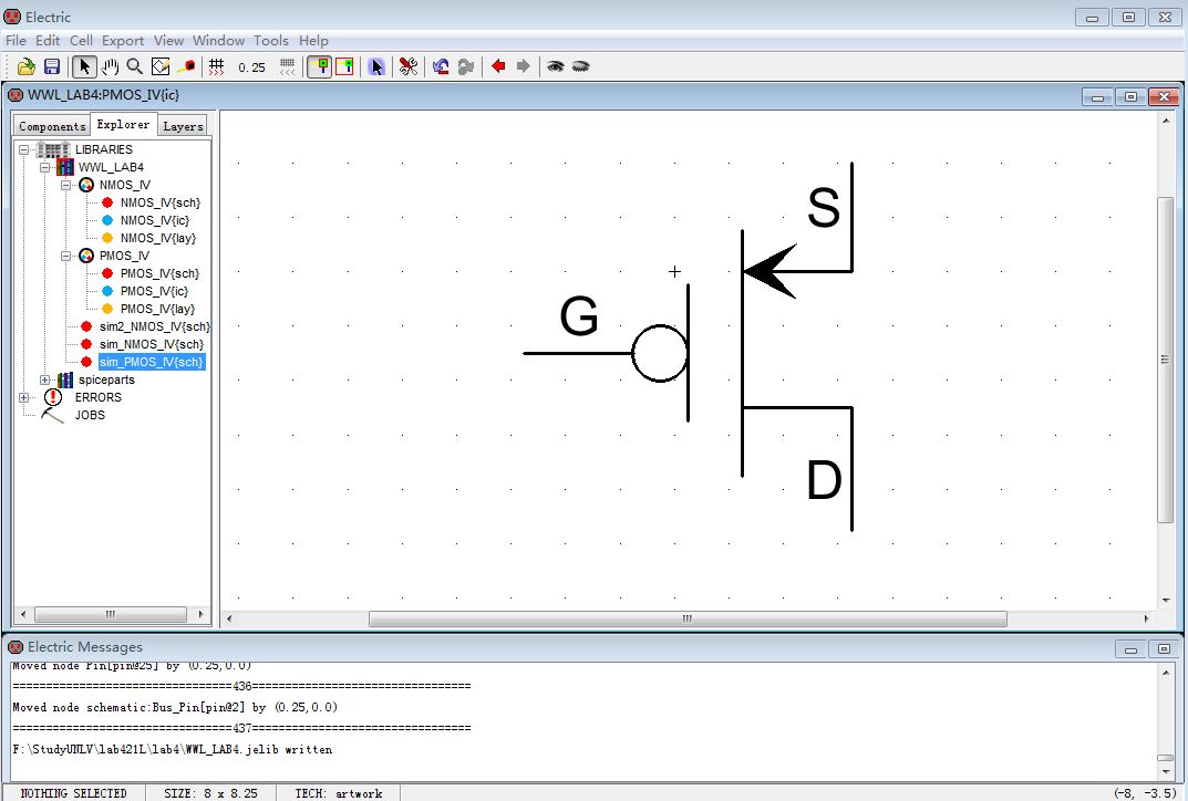
Finally, we need to name the exports, gate, drain, source. In the tutorial_2, we use lowercase"g,d,s". I change the exports into "G,D,S" and delete the spice code, as shown in the following images. Make sure that DRC, ERC, NCC are passed.

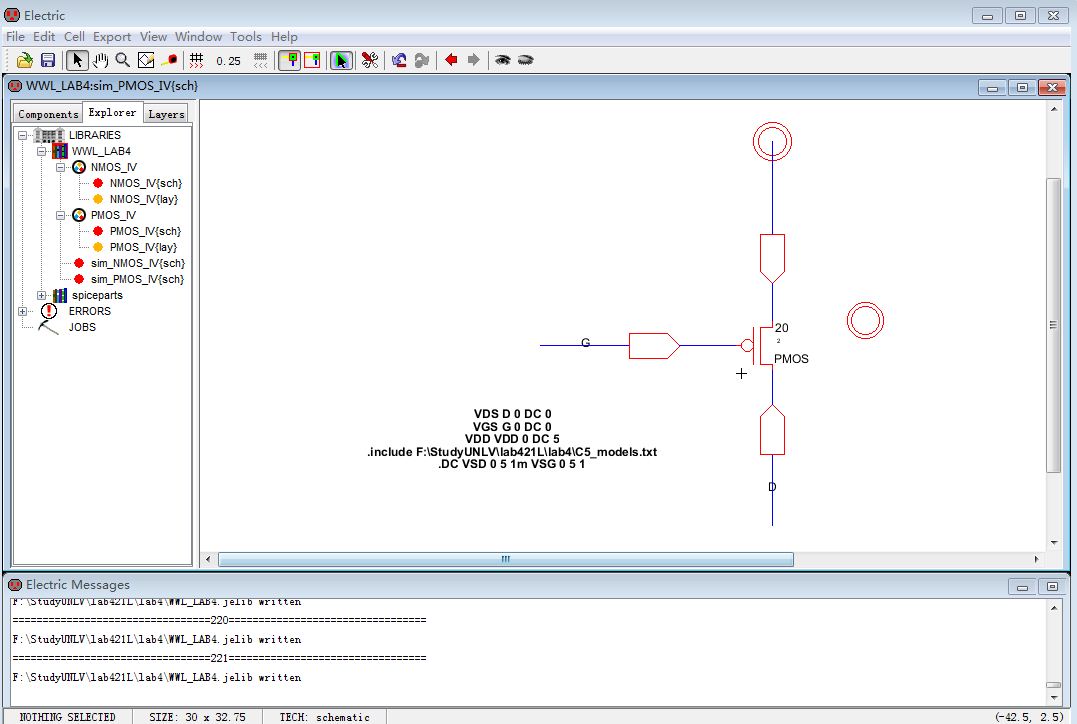
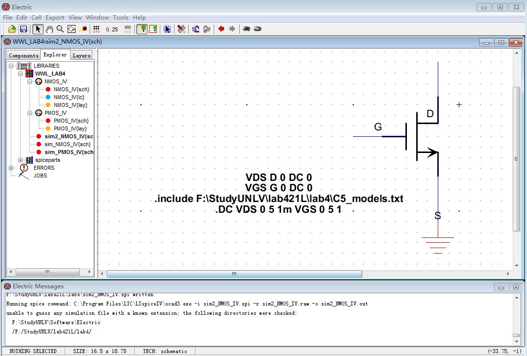
5.) Then create two new cells to simulate the schematic: sim_NMOS_IV and sim_PMOS_IV. Drag the respective schematic cell into the simulation cells without making icons. Connect a gnd to source node of NMOS(connect vdd to source node of PMOS) and wire arcs are connected to drain and gate with names(they are not exported.)
Put the spice code in the simulation cells and run the simulations to see the results.

6.) Next, try to make icons for NMOS and PMOS. Go to View--> Make Icon View. Select black point in the components menu. Put one black points in the icon view. Click the black line. Then left click the black point and right click to other place to make a line. Make the NMOS(PMOS) typical symbol as seen below. These three exports should be put in the right position. The PMOS icon also uses the black circle.


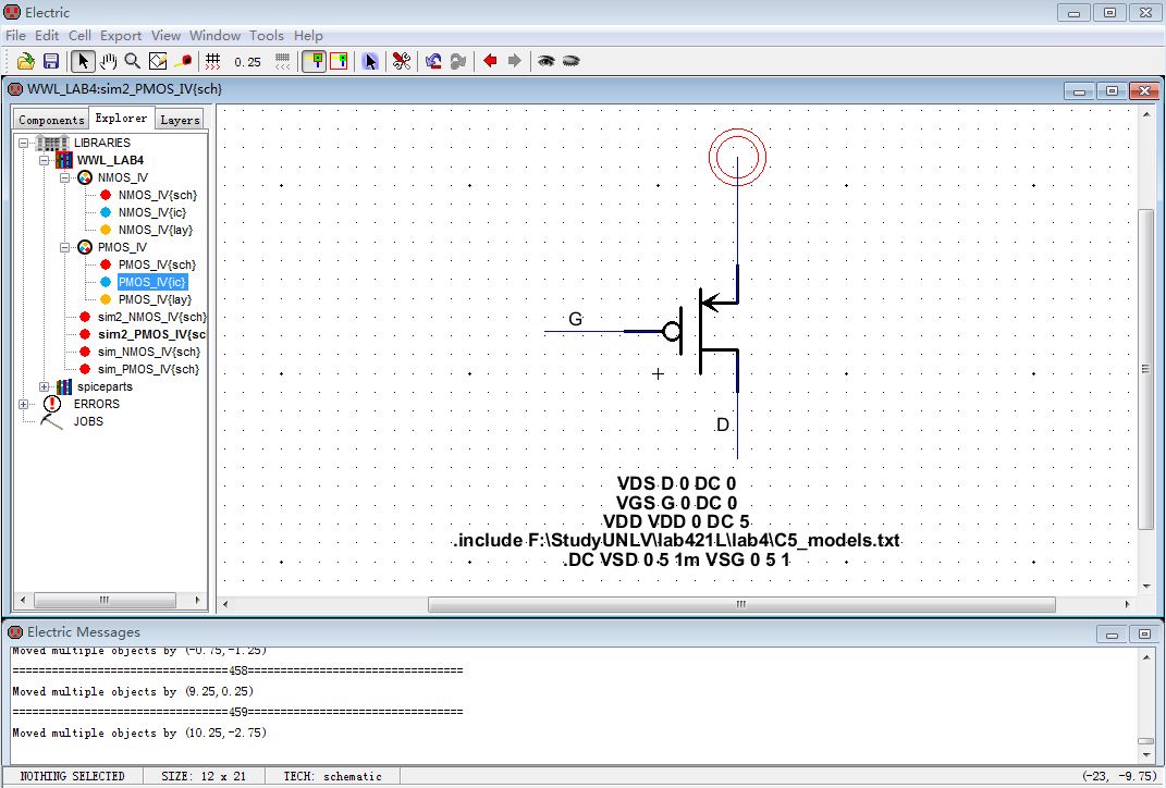
7.) Use the icons to create the another simulation cells.
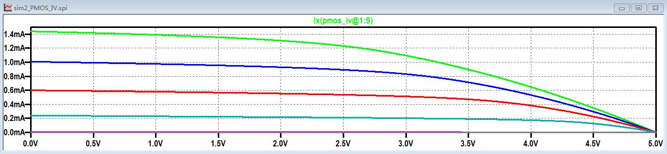
8.) Run the simulation and get the following result. Before simulating the schematic, make sure design has passed DRC, ERC, and NCC.

Backup the work directory for future study
