 Lab 7 – EE 420L
Authored by: Daniel Senda
Email: sendad1@unlv.nevada.edu
Spring 2019
Due: 04-03-2019
1) Pre-Lab Description
The pre-lab
required the student to review lab 6 in order to
prepare for this lab.
2) Description of Lab
Procedures
This lab
required the student to design an audio amplifier. The following are the
requirements that the student had to meet:
- Frequency range: 100Hz to 20kHz.
- Input resistance: A few kilo-ohms (It should be able
to take an audio input signal from an MP3 player or similar)
- Output resistance: Less than 1 ohm (Since design is
connected to an 8-ohm speaker)
- Supply voltage: 10V (5V was used for reasons
explained later)
- Circuit must contain only one 10uF
capacitor and one 100uF capacitor.
- Student can use as many resistors and
transistors (ZVN3306A and ZVP3306A) needed.
In addition,
the student was also required to:
- Describe the design of the amplifier
including hand calculations.
- Simulate the design and show results.
- Build and test the design.
- Document the performance of the
amplifier design.
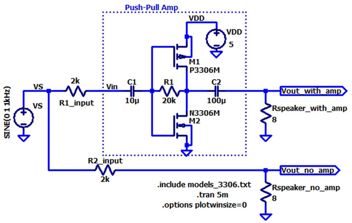
Student’s Audio Amplifier Design:
The student
decided to design the audio amplifier using the push-pull topology. The basic
push-pull topology has two MOSFETs in it as seen in the circuit schematic
below. The PMOS on the top sources current while the NMOS on the bottom sinks
current. These work together to “push” and “pull” current at the output through
the load. Push-pull amplifiers also have a small input resistance compared to
other amplifiers, which helps meet one of the requirements.
Push-pull audio amplifier circuit
schematic:
Hand calculations:
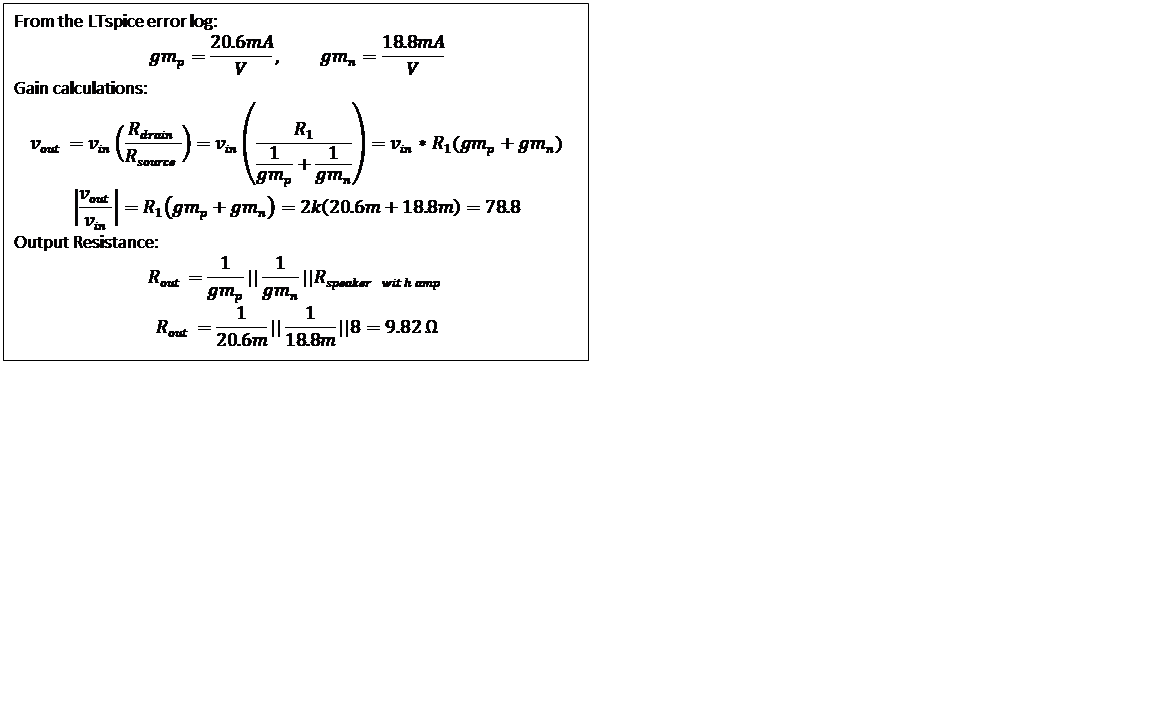
The previous
calculation is for an amplifier with no load on the output. When there is an
8-ohm load on the output (speaker 1), the gain is not an obvious thing to see
in simulations or experiments. Therefore, the student decided to also add a
second part to the circuit where the signal is not amplified and connected
straight to the 8-ohm load (speaker 2). The secondary output (with no amplifier)
can be used to compare with the primary output (with an amplifier) to visually
see the gain.
Audio amplifier simulation results:
The following are
simulation results which show the circuit is doing what it was designed to do,
which is to amplify the input signal to drive an 8-ohm speaker. The circuit
that is simulated is the exact one pictured previously.
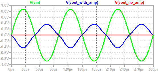
Simulation 1 (Frequency at min value
of 100Hz):
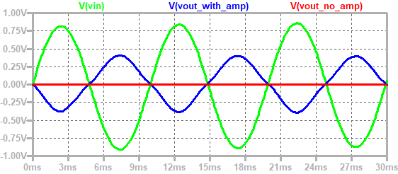
Simulation 2 (Frequency at min value
of 1kHz):
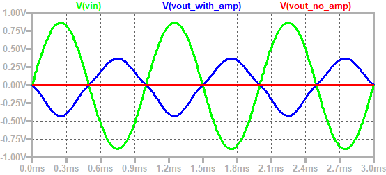
Simulation 3 (Frequency at min value
of 10kHz):
Simulation 4 (Frequency at min value of
20Hz):
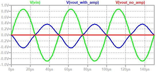
As can be
seen, the amplifier is operational in the required frequency range.
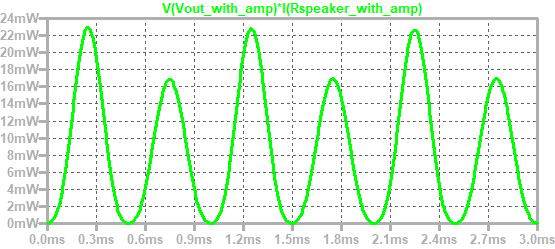
Power dissipation through speaker
with amplifier:
Power dissipation through speaker
with no amplifier:
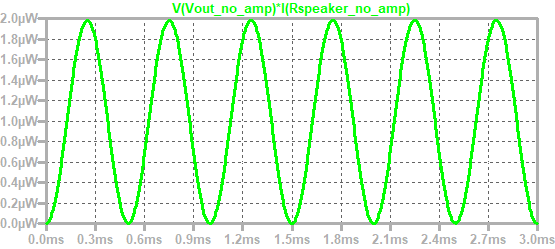
The power
dissipated through the speaker with the audio amplifier is higher, as expected.
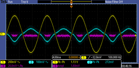
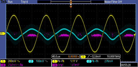
Experimental Results of Built Audio Amplifier:
The audio
amplifier design was built on a breadboard and the following are snapshots of
the outputs the student got on the oscilloscope. The yellow signal is the
input, the blue signal is the output of the speaker with the audio amp, and the
pink signal is the output signal of the speaker with no amp.
Experiment 1 (Frequency at min value
of 100Hz):
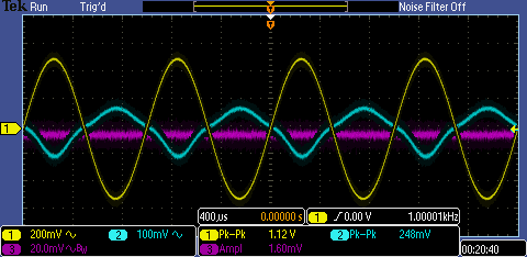
Experiment 2 (Frequency at min value
of 1kHz):
Experiment 3 (Frequency at min value
of 10kHz):
Experiment 4 (Frequency at min value
of 20Hz):
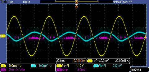
As can be
seen also been seen through the experimental results, the amplifier is
operational in the required frequency range.
The student
took video of the audio amplifier
outputting music, which shows that the design was successful.
This
concludes lab #7.
Additional Links
→ Return to listing of
lab reports
→ Daniel’s CMOS
homepage
→
Dr. Baker’s CMOS homepage