 Lab 6 – EE 420L
Authored by: Daniel Senda
Email: sendad1@unlv.nevada.edu
Spring 2019
Due: 03-27-2019
1) Introduction
This lab
introduces students to the different types of amplifiers. The procedures have
the student work with four different topologies that include: Source follower/
(Common Drain) amplifiers (NMOS and PMOS), Common source amplifiers (NMOS and
PMOS), Common gate amplifiers (NMOS and PMOS), and Push-pull amplifiers.
2) Pre-Lab Description
The pre-lab
required the student to complete the following before proceeding with lab:
- Read through the datasheets of the
N-Channel DMOSFET (ZVN3306A)
and of the P-Channel DMOSFET (ZVP3306A)
and become familiar with them.
- Simulate the circuits given in the lab6_sims.zip
file and understand operation and verify that the simulations reasonable model
the behavior of the transistors.
- Watch the single_stage_amps video and read single_stage_amps.pdf
review.
3) Description of Lab
Procedures
This lab
utilizes the N-Channel DMOSFET and of the P-Channel DMOSFET mentioned above.
The lab had
the student work with four circuit configurations which include:
- Source follower/ (Common Drain)
amplifiers (NMOS and PMOS)
- Common source amplifiers (NMOS and
PMOS)
- Common gate amplifiers (NMOS and
PMOS)
- Push-pull amplifier
For the
first three configurations listed, the student was instructed to hand calculate
the gains, input resistances, and output resistances.
These
circuits were built using electrolytic capacitors. An electrolytic capacitor
has polarity; in simple terms it means that it has a positive and a negative
side. These should not be put in backwards because it can cause harm to the
capacitor making is useless. The positive side of the electrolytic capacitor
should be connected to the higher DC potential (voltage) in the circuit. This
will ensure proper operation.
The
experimental gain of a circuit can found by taking the magnitude of the output
(Vout) and dividing it by the magnitude of the input
(Vin).
The
experimental input resistance can be calculated by the following way:
- First, the theoretical input
resistance needs to be calculated. Once the theoretical resistance is
calculated, a resistor of that value should be connected in series between the
input voltage (Vin) and the AC coupling capacitor (input capacitor).
- Second, calculate the AC current
going through the added resistor. This can be accomplished by measuring the AC
voltage (magnitude) on the Vin side of the resistor and measuring the AC
voltage (magnitude) on the capacitor side of the resistor. Take the difference
between these measurements and divide this difference by the value of the added
resistor, thus resulting in the AC current (magnitude) value.
- Third, find the amplifier’s input
resistance. This can be accomplished by measuring the AC voltage (magnitude) at
the input of the amplifier (the other side of the ac coupling capacitor not
connected to the added resistor). Then divide this AC voltage (magnitude) by the
AC current (magnitude) solved for previously, which results in the value of the
amplifier’s input resistance.
The
experimental output resistance can be calculated the following way:
- First, the theoretical output
resistance should be calculated. Once this value is obtained, a resistor of
that value should be connected in series with big capacitor (to avoid messing
up the DC biasing) and added between the output of the amplifier and ground.
- Second, calculate the AC current flowing
through this added resistor. This can be accomplished by measuring the AC
voltage (magnitude) across the resistor and dividing that by the value of the
added resistor.
- Third, find the amplifier’s output
resistance. This can be accomplished by measuring the AC voltage (magnitude) on
the gate of the MOSFET and the AC voltage (magnitude) on the source of the
MOSFET. Then take the difference of these two measurements and divide this
value by the AC current value previously calculated, which results in the value
of the amplifier’s output resistance.
The
following sections discuss all of the listed circuits along with calculations,
simulations, and experimental results.
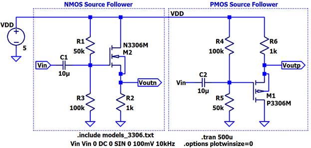
NMOS and PMOS Source Follower (Common Drain) Amplifiers
These
amplifiers are called source followers because the input and output closely
resemble each other. The gain of this non-inverting topology is one, which
explains the resemblance between the input and output. These tend to have a
high input resistance and low output resistance.
LTspice circuit schematic:
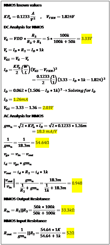
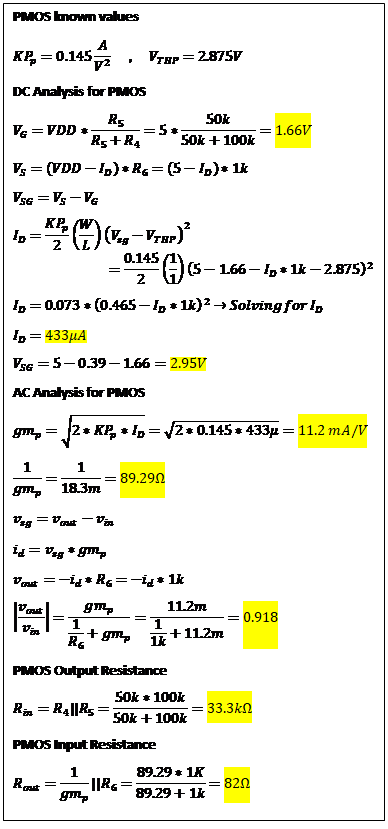
NMOS Hand Calculations:
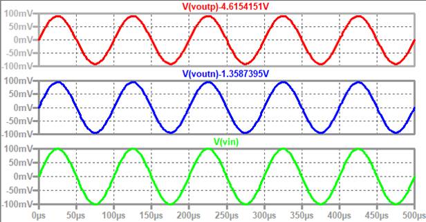
NMOS and PMOS LTspice
simulation results:
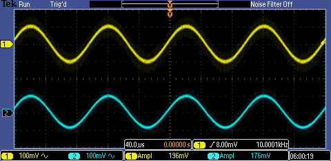
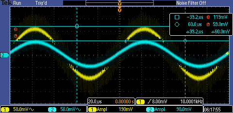
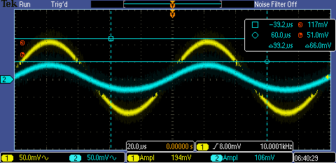
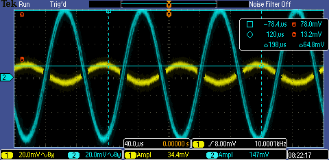
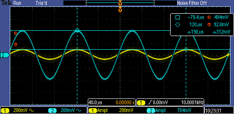
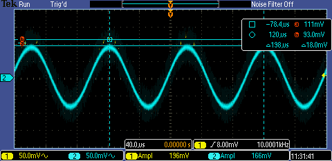
NMOS Experimental Results:
Shows gain
of NMOS configuration which is essentially 1, no added resistor.
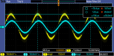
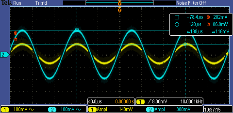
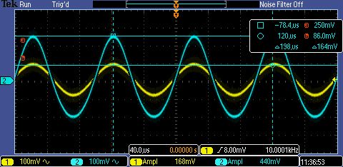
Shows input
resistance results, with added resistor of 32.3k. The output is half the input.
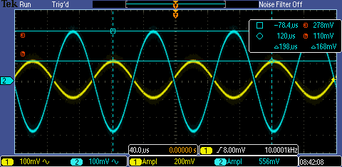
Shows output
resistance results, with added resistor of 50.56. The output is half the input.
The
following table displays the theoretical and experimental results for the NMOS.
|
Data Type |
Gain |
Rin Ω |
Rout Ω |
|
Theoretical |
0.948 |
33.3k |
52 |
|
Experimental |
1 |
31.7k |
65.4 |
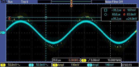
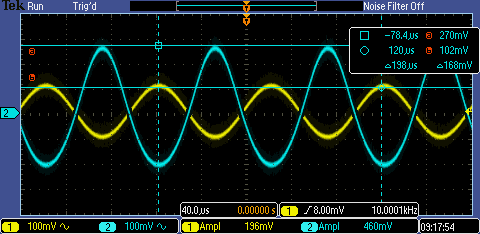
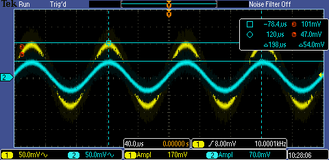
PMOS Experimental Results:
Shows gain
of PMOS configuration which is about 0.78, no added resistor.
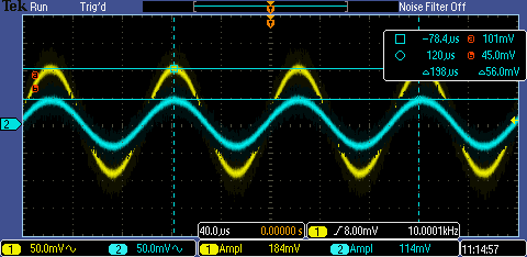
Show input
resistance results, with added resistor of 32.2k. Output is half the input.
Shows output
resistance results, with added resistor of 179. Output is half the input.
The
following table displays the theoretical and experimental results for the PMOS.
|
Data Type |
Gain |
Rin Ω |
Rout Ω |
|
Theoretical |
0.918 |
33.3k |
82 |
|
Experimental |
0.78 |
27.4k |
170 |
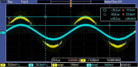
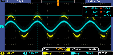
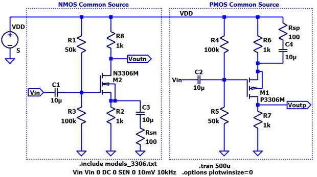
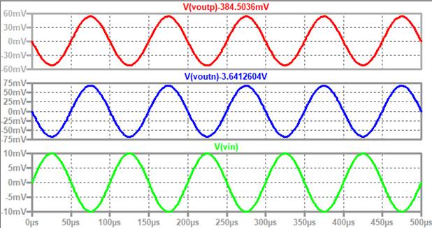
NMOS and PMOS Common Source Amplifiers
These
amplifiers are called common source amplifiers because Vin
and Vout are common at the source.
LTspice circuit schematic:
NMOS and PMOS LTspice
simulation results:
NMOS Experimental Results:
NMOS
configuration shows a gain of 6 when Rsn it changed
to 50 ohms instead of 100 ohms. 100 ohms created a gain of 4.5.
Shows input
resistance results, added resistor of 32.3k.
Shows output
resistance results, added resistor of 1k. Has expected gain of about 2.5.
PMOS Experimental Results:
PMOS
configuration shows gain of about 2.7
Shows input
resistance results, added resistor of 32.3k.
Shows output
resistance results, added resistor of 1k. had an expected gain of about 1.3.
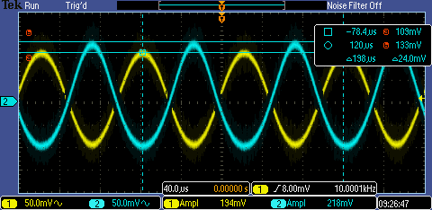
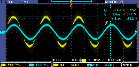
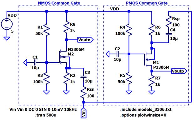
NMOS and PMOS Common Gate Amplifiers
LTspice circuit schematic:
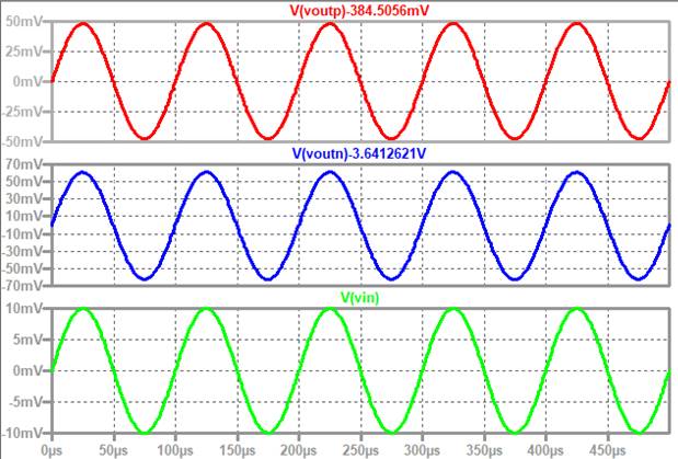
NMOS and PMOS LTspice
simulation results:
NMOS Experimental Results:
NMOS
configuration shows a gain of about 4.39, no resistor added.
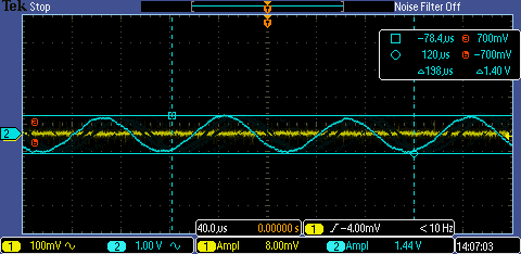
Shows input
resistance results, added resistor of 198.7.
Shows output
resistance results, added resistor of 1k.
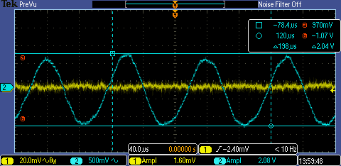
PMOS Experimental Results:
PMOS
configuration shows a gain of 2.42.

Shows input
resistance results, added resistor of 413.
Shows output
resistance results, added resistor of 1k. Has a gain of 0.84, slightly lower
than expected. Theoretical gain is 1.21.
If Rsp is decreased to 50 ohms, the gain increases.
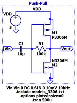
Push-Pull Amplifier
LTspice circuit schematic:
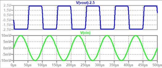
LTspice simulation results:
Experimental Results:
Gain with
resistor of 100k:
Gain with
resistor of 510k:
This
concludes lab 6.
Additional Links
→ Return to listing of
lab reports
→ Daniel’s CMOS
homepage
→
Dr. Baker’s CMOS homepage