EE
421L Digital Integrated Circuit Design -
Lab 8
Generating
a test chip layout for submission to MOSIS for fabrication
Pre-lab
work
- Back-up all of your
work from the lab and the course.
- Download the bare pads
for a tiny-chip (1.5 mm x 1.5 mm with 40 bond pads) seen here.
- Use a cross-library
copy to copy these pads into your lab jelib.
- Ensure
that your lab jelib
is not linked to any other jelib
by copying it into a different directory, re-starting Electric, and
opening the copied jelib.
Form
into groups of 4 students that will put the test structures on the chip.
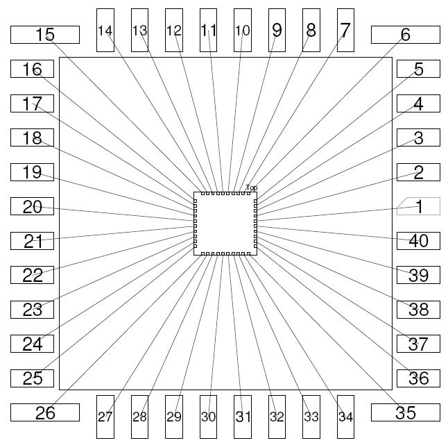
Use pin 20 for grounding the substrate and providing ground for all of
the
circuits on the chip, see DIP (dual in-line package) bonding diagram
below for
pad locations.
Each test circuit should have its own power (VDD) but ground should be
shared
between the circuits.
Power should not be shared between the circuits so that
a VDD-gnd
short in one circuit doesn't make one of the other
circuits inoperable.
Your report, and final chip layout, are due near the beginning of the lab at which time I may submit the chip for fabrication.
Your chip should include the following test structures:
- 100/2 NMOS (3 pins,
DN, GN, SN, connect the p+ body, B, of the NMOS to the chip's ground
pin)
- 100/2 PMOS (4 pins,
DP, GP, SP, and BP)
- Inverter made using
100/2 NMOS and 200/2 PMOS (3 pins, in, out, VDD_inv)
- 61 stage ring
oscillator using 10/2 MOSFETs with off-chip buffer (2 pins, VDD_osc and Ocs_out. Ground connected to pin
20)
- 20k n-well resistor (2
pins)
- 20k hi-res poly
resistor (2 pins)
- 1k n+ resistor (2 pins)
- 1k p+ resistor (3
pins, need n-well to isolate the p+ from the p-substrate and the n-well
needs to be tied to a voltage >= either side of the resistor)
- Bandgap reference (2 pins, VDD_bg and Vref)
- Whatever else you
would like to fabricate to use the remaining pins on the chip
- Feel free to "sign"
the chip or add a graphic (see the bottom of this webpage).
Use the DRC exclusion layer to ensure the final chip still passes DRCs.
- Also note
that you can reduce the number of pins needed by sharing some
of them (e.g., you really only need 3 pins for the n-well and hi-res
poly resistors). Since only one test structure will be tested at a time
this savings can be significant. The savings of pins may be
useful if you want to fabricate your lab projects.
In your CMOSedu.com lab account create a directory called lab8.
Create a jelib called MOSIS_chipX
where X is a number the lab instructor will assign after the groups are
formed.
Put the details of your chip (how to test it) in your lab report in
this
directory.
Schematics with pin numbers and SIMPLE directions on how to test the
chips
should be the main content of these reports.
If your group's chip is fabricated it will be tested the next time the
lab is
taught.
MOSIS returns 5 packaged chips for each design submitted for
fabrication so it's possible that each member of a group, as
long as
they test the chip and report on how it worked, can get a chip
to keep.
Your report should include a link to your MOSIS_chipX jelib
file (for future reference).
This jelib should be
"clean" meaning that
it only contains the cells (schematics, icons, layouts, and
simulations) used
in the final chip.
The top level cell, the one that will be fabricated, should be called topX and have both schematic and layout views so it can be NCCed, DRCed, and well-checked.
Each student must have a lab8 html lab report in their lab8 directory
at CMOSedu.com;
however, feel free to copy from each other.
If you use the same html report that is okay as long as all students
names are
listed on it and all students contributed to the design of the chip.
Again, ensure that your html lab report includes your name, and the
names of
the other students in your group along with your email
addresses at the beginning of the report (the top of the webpage).
When finished backup your work (webpages
and design
directory).