Some random
information related to using Eagle for the layout of printed circuit (PC)
boards.
Eagle Cad
Tutorials (a total of 12) http://www.youtube.com/watch?v=qG0O9LKH-_E (great to get
going quick!)
A tutorial video
covering the use of Eagle done by Lincoln Bollschweiler here.
Pin headers Eagle library "pinhead"
End connection
SMA connectors Eagle Package J502-ND-142-0701-801/806
Value SMA-142-0701-801/806
A layout and
symbol for mounting a tiny chip from MOSIS to a PC board is found here. Note that this library defines pin 1
on the left/top of
the padframe. Pin 10 is on the left/bottom.
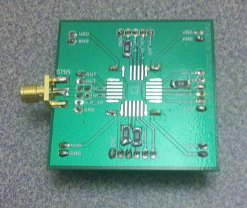
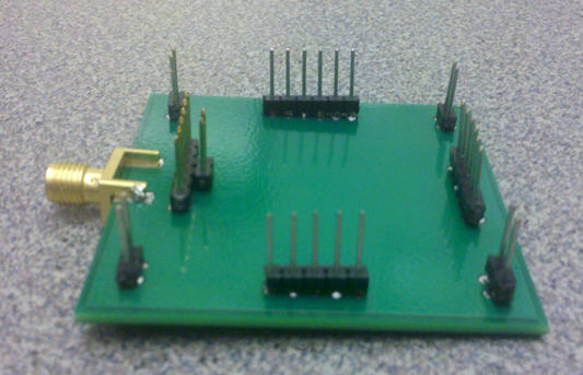
A board for
testing the KD1S_test_chips seen here is available in KD1S_Test_Board.zip. A 50-ohm
feedthru BNC was used
to terminate
analog input and clock signals and a BNC
to SMA adapter is used to go from the co-ax to the SMA end connectors
on the board.
How to solder
introduction http://www.youtube.com/watch?v=I_NU2ruzyc4
How to solder
SMD http://www.youtube.com/watch?v=3NN7UGWYmBY
Information on
making a symbol from scratch is found here.
Some information
on bonding a chip to the PC board.
It’s good if the
board can be made so that it rests flat. Below the pin headers are placed on
the back side of the board to
provide a flat
surface. Note that the top of the board, the left image, is fairly flat so that
the wire bonder can access the chip
without hitting a
component.
Using Al wire and
the lowest (on the wire bonder) power setting may work best for bonding the
chip to the board. Try to make the
traces on the
board as small as possible. Also, Ablebond 84-3 is
used to glue the chip to the board (see bondingsource.com).