Digital Integrated Circuit DesignEE 421L - Fall 2021
Lab 5
Author: Ryan Eclarinal
Email: eclarina@unlv.nevada.edu
Date Assigned: September 22, 2021
Due Date: October 6, 2021
Pre-Lab:
- Go through Tutorial 3.
In this tutorial we were ask to draw the schematic, symbol, and layout of a CMOS inverter.
We were also need to do a simulation of the DC behavior of the inverter.
Schematics of the CMOS Inverter:
I
copied the nmos and the pmos from Tutorial 2 and also instantiated vdd,
gnd and pins. I connected everything with wire to form the CMOS
inverter and then saved it.

After saving the schematics, I created a symbol and saved it.

The next step is to create a layout of the inverter using 12u/.6u PMOS, 6u/.6u NMOS, ntap, ptap, and m1_poly.
Layout View of the Inverter:


After completing the inverter, we need to run DRC to make sure that the layout doesnt have any errors.
Once this is done, the next step is to extract the layout.
Extracted View of the Inverter:

We are ready to run the LVS for the layout view and the extracted view to make sure that everything matches.
Running the LVS: The figure below shows that the net-list matched.

The output log of the result.

Simulation:
First, we need to create a new schematic on a new cell called sim_inverter_dc.
Launching the ADE:


Result of the simulation showing no output.

To correct this, we need to put vdd! on the schematic and setup analog
stimuli. It is basically a global "power supply" that will add voltage
to the input.


Rerunning the simulation will get this result.

Showing that we are running the extracted layout will give us the same result.


Tutorial 3 done.
Lab 5 - Design, layout, and simulation of a CMOS inverter
Experiment 1: Schematic, Layout and Symbol for 12u/.6u PMOS and 6u/.6u NMOS
Schematic of the 12u/6u inverter:

Creating the Symbol for the 12u/6u inverter 
Layout view and Extracted view of the inverter

Running LVS and showing that the net lists matched.

Output log of the result.

Experiment 2: Schematic, Layout and Symbol for 48u/.6u PMOS and 24u/.6u NMOS
Schematic of the 48u/24u inverter:

Creating the Symbol for the 48u/24u inverter

Layout view and Extracted view of the inverter 

Running LVS and showing that the net lists matched.

Output log of the result.

Experiment 3: Simulation for the 12u/6u inverter
Schematics of the 12u/6u inverter
Launching the ADE and setting the correct parameters:

Running the Parametric Analysis using SPECTRE simulation:

Result of the simulation:
Creating the labels for the different values of the capacitors

Running the Parametric Analysis using UltraSim:

Result of the simulation:
Experiment 4: Simulation for the 48u/24u inverter
Schematics of the 48u/24u inverter

Launching the ADE and setting the correct parameters:


Running the Parametric Analysis using SPECTRE simulation:

Result of the simulation:

Running the Parametric Analysis using UltraSim:
Result of the simulation:

Backing up:
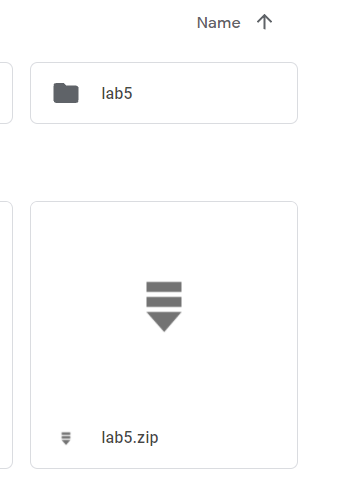
Perform a regular back up of my work by making a zip file and upload it to my Google Drive.


This concludes Lab 5
The files on this lab can be downloaded here.
Return to Students
Return to EE 421L
Return to CMOSedu.com


