Digital Integrated Circuit DesignEE 421L - Fall 2021
Lab 4
Author: Ryan Eclarinal
Email: eclarina@unlv.nevada.edu
Date Assigned: September 15, 2021
Due Date: September 22, 2021
Pre-Lab:
- Go through Tutorial 2.
- In
the simulations in this lab the body of all NMOS devices (the
substrate) should be at ground (gnd!) and the body of all PMOS devices
(the n-well) should be at a vdd! of 5V.
Following the Tutorial 2:


Creating the schematic and symbol for the MOSFET(nmos) with the width of 6um and length of 600nm.


Creating another schematic for our circuit using the symbol that we created.

Running the Parametric Analysis will get this result.

Now,
we build our NMOS layout and add the pins S, D, G, and gnd!. After
doing the DRC and there is no error, we need to extract our layout.


We are ready to do the LVS and here showing that the net-list matched.


Showing that we are running the extracted layout will give us the same result.

Creating the schematic and symbol for the MOSFET(pmos) with the width of 12um and length of 600nm.


Creating another schematic for our circuit using the symbol that we created.

Running the Parametric Analysis will get this result.

Now, we build our PMOS layout
and add the pins S, D, G, and B. After doing the DRC and there is no
error, we need to extract our layout.


We are ready to do the LVS and here showing that the net-list matched.


Showing that we are running the extracted layout will give us the same result.

Lab 4 - IV characteristics and layout of NMOS and PMOS devices in ON's C5 process
Experiment 1:
We need to generate a schematic for simulating ID
vs VDS of an NMOS device for VGS varying from 0 to 5 V in 1 V steps
while VDS varies from 0 to 5 V in 1 mV steps. Here we use a
6u/600n width-to-length ratio.
Our schematic

Here showing how to set the parameters so we can run the simulation.

Running the Parametric Analysis will give us this result.


Experiment 2:
We need to generate a
schematic for simulating ID v. VGS of an NMOS device for VDS = 100 mV
where VGS varies from 0 to 2 V in 1 mV steps. Again, we use a 6u/600n
width-to-length ratio.
Our schematic

Here showing how to set the parameters so we can run the simulation.

Running the Parametric Analysis will give us this result.


Experiment 3:
We need to generate a
schematic for simulating ID v. VSD (note VSD not VDS) of a PMOS device
for VSG (not VGS) varying from 0 to 5 V in 1 V steps while VSD varies
from 0 to 5 V in 1 mV steps. Here we use a 12u/600n width-to-length ratio.
Our schematic

Here showing how to set the parameters so we can run the simulation.

Running the Parametric Analysis will give us this result.

Experiment 4:
We need to generate a
schematic for simulating ID v. VSG of a PMOS device for VSD = 100 mV
where VSG varies from 0 to 2 V in 1 mV steps. Again, we use a
12u/600n width-to-length ratio.
Our schematic

Here showing how to set the parameters so we can run the simulation.

Running the Parametric Analysis will give us this result.

Making a Probe Pad:
We need to create our own probe pads and we need to follow the MOSIS Design Rules which you can check here, page 53.
Creating the glass layer first then draw a rectangle using Metal 3 layer.

I use the 12um x 12um for my glass layer and 24um x 24um for my metal3 layer.

Here showing the 6um clearance between the glass layer and the metal3 layer according to the design rule.

Check and save the layout.
Now we need to create a schematic for our probe pad.

After creating the schematic, we need to create a symbol.

Now we will continue our experiment.
Experiment 5:
We
need to lay out a 6u/0.6u NMOS device and connect all 4 MOSFET
terminals to probe pads (which can be considerably smaller than bond
pads and directly adjacent to the MOSFET).
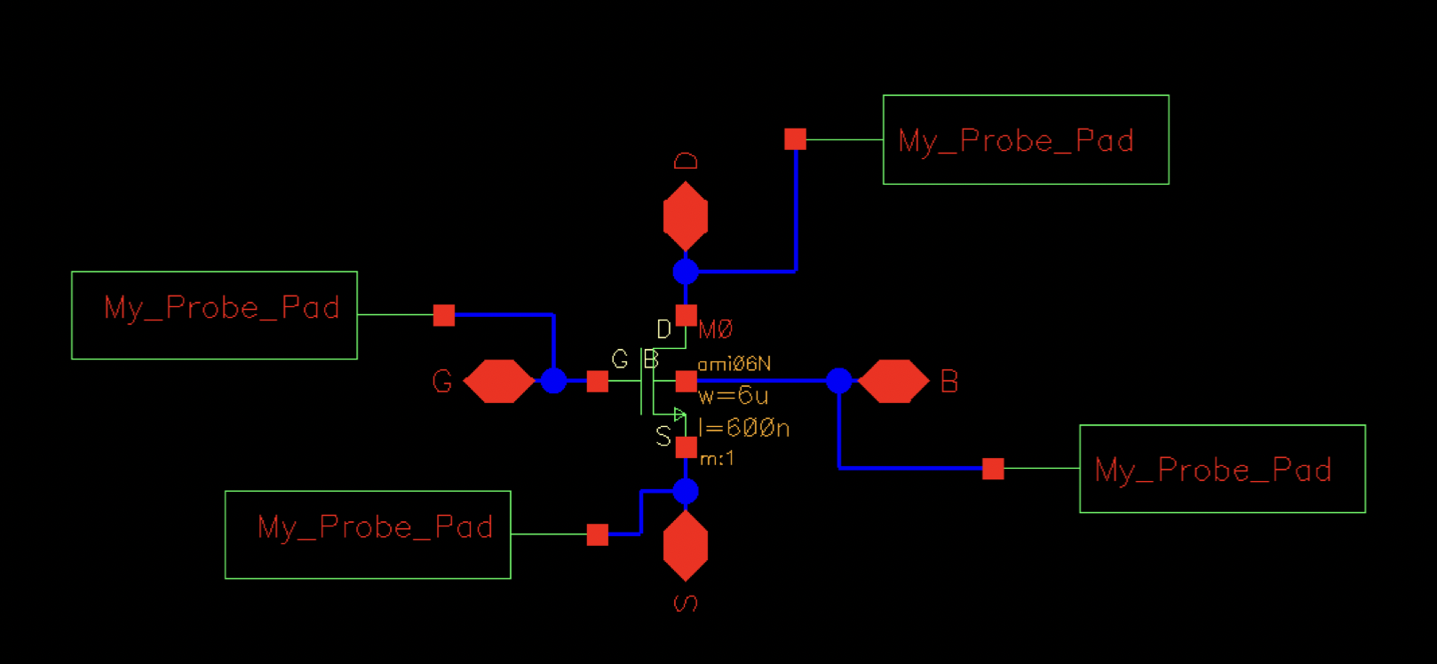
Here, showing the schematics and connecting the probe pad symbol that we created to each pins.
Now, we go to our layout and mirror the steps that we did on our schematics. Instantiate the probe pad on the layout.

After connecting all the MOSFET terminals to the probe pads, we DRC our work to make sure that there is no error.

Here, showing how we connected our layers of metal. From metal2 to metal1, we use via1 and from metal3 to metal2, we use via2.

Since there is no error after we did the DRC, we can now extract our layout.

We can now run the LVS to show that the net-list matched.


Rerun Experiment 1 with this new schematics which the body has been connected.

Running the Parametric Analysis successfully with the probed NMOS layout.

Here, we verified that the extracted layout ran first. (Simulation -> Netlist -> Display)

Experiment 6:
We need to lay out a 12u/0.6u PMOS device and connect all 4 MOSFET terminals to probe pads.
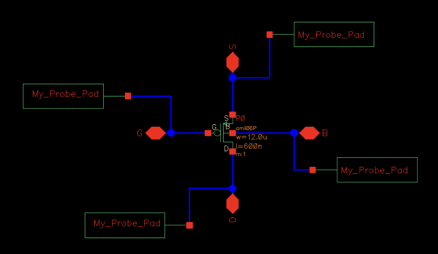
Here, showing the schematics and connecting the probe pad symbol that we created to each pins.
Now, we go to our layout and mirror the steps that we did on our schematics. Instantiate the probe pad on the layout.

After connecting all the MOSFET terminals to the probe pads, we DRC our work to make sure that there is no error.

Since there is no error after we did the DRC, we can now extract our layout.

We can now run the LVS to show that the net-list matched.


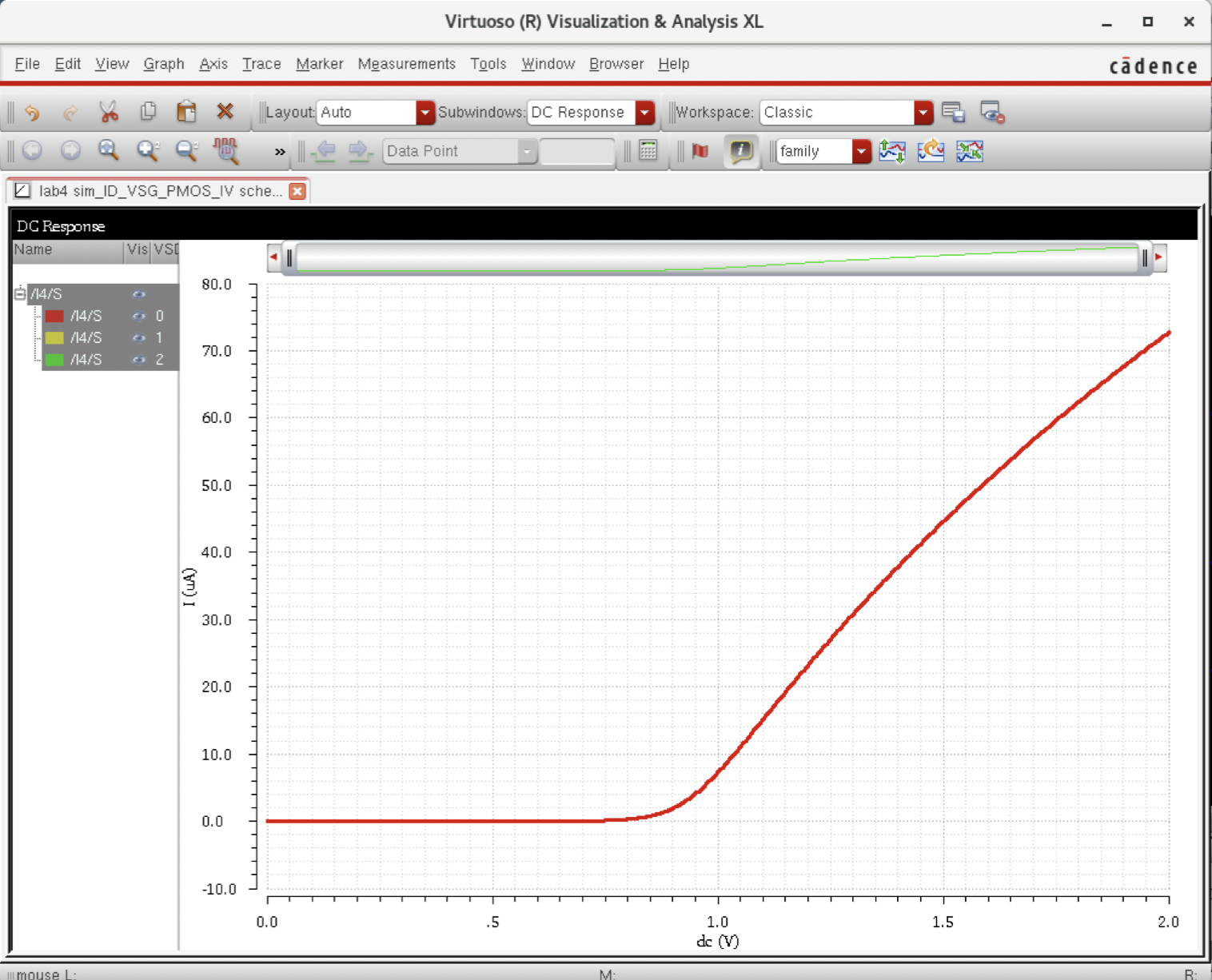
Running the Parametric Analysis successfully. Here, we verified that the extracted layout ran first. (Simulation -> Netlist -> Display)
Backing up:
Perform a regular back up of my work by making a zip file and upload it to my Google Drive.


This concludes Lab 4.
Return to Students
Return to EE 421L
Return to CMOSedu.com