Lab 4 - EE 421L
Damian Aceves-Franco
acevesfr@unlv.nevada.edu
09/14/2021
**********************
Lab
September 15 – Lab4 – IV characteristics and layout of NMOS and PMOS devices in ON's C5 process, due September 22
*********************
Pre-lab work
- Back-up all of your work from the lab and the course.
- Read through this lab before starting it.
- Go through Tutorial 2 seen here.
- In
the simulations in this lab the body of all NMOS devices (the
substrate) should be at ground (gnd!) and the body of all PMOS devices
(the n-well) should be at a vdd! of 5V.
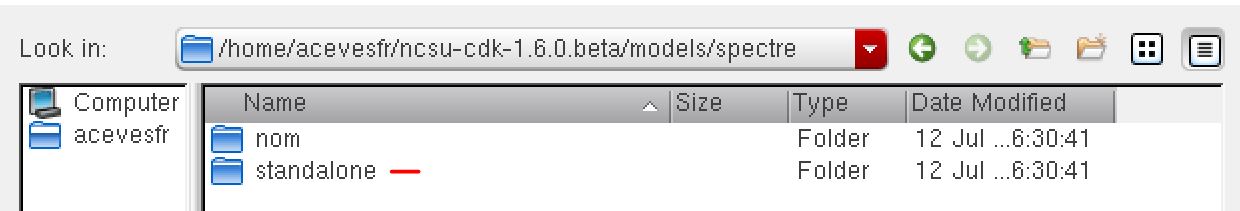
Creat
a new library and creat a new schematic with the NMOS provied from the
NCSU_Analog_Parts it must be 6u/600n and place pins
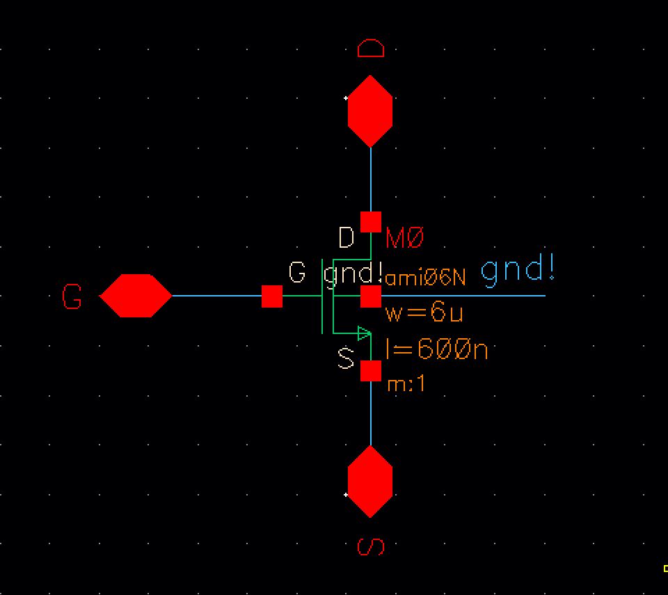
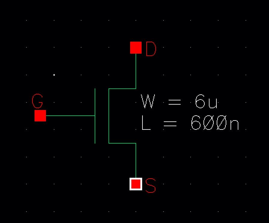
then we save the schemaic and creat and symbol. Deleting everything but the pin and redrawing the Mosfet
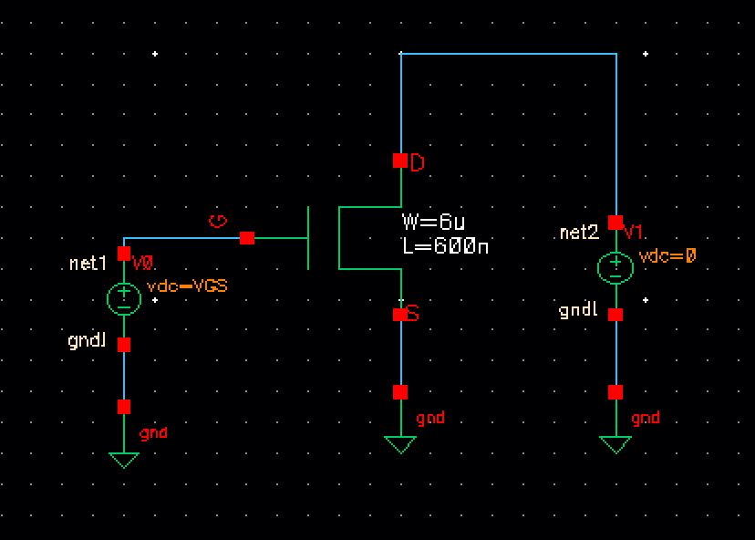
then we make a schemic layout with the symbol and creating the folloing circuit. Make sure to make vdc=VGS at V0
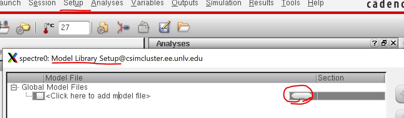
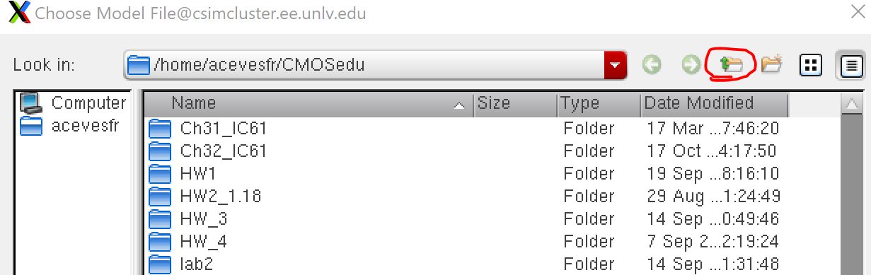
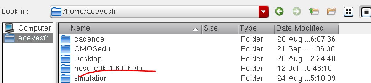
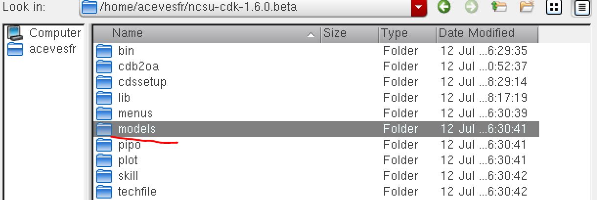
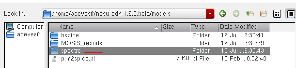
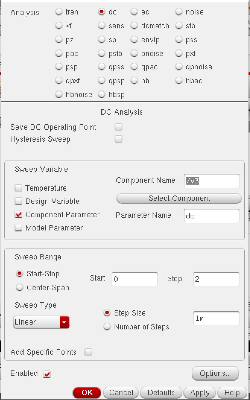
then lunch ADE and setup the Model Library
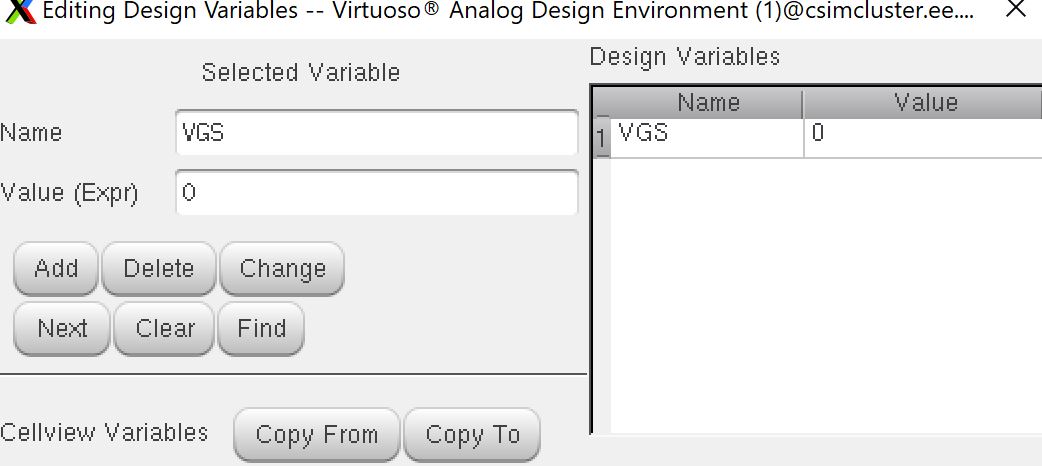
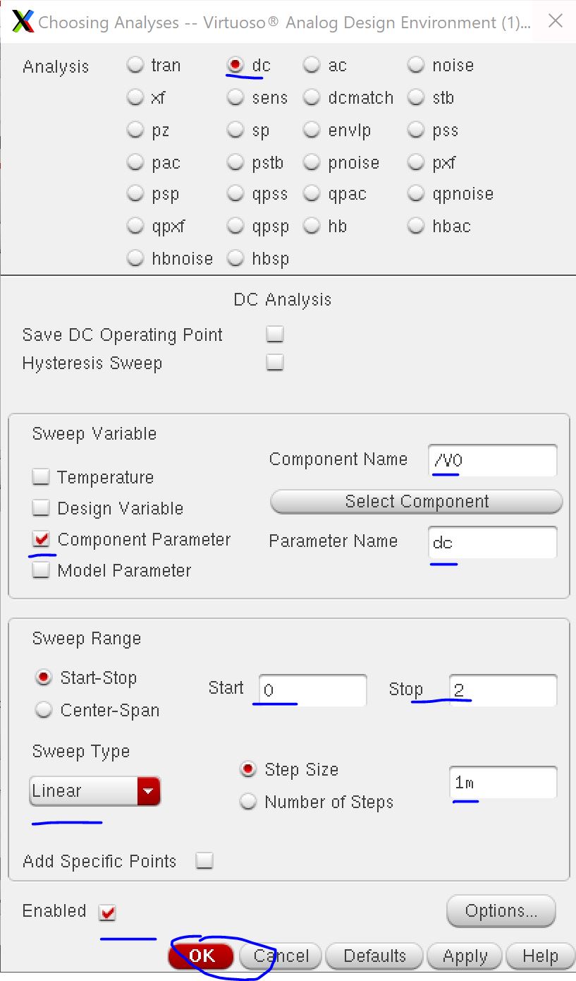
then in the ADE go to Variables ->Edit and add the variable VDS with Value 0 then ok
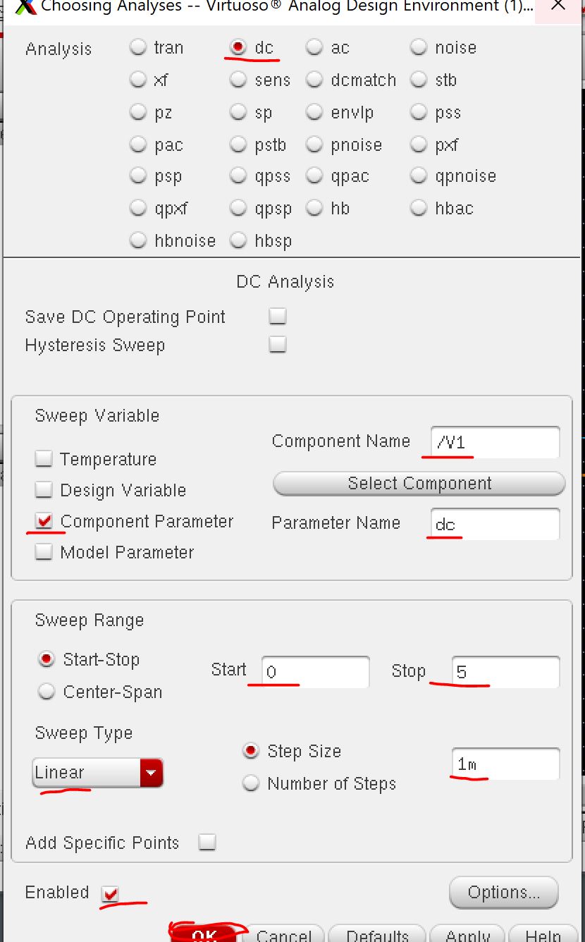
then in ADE go to Analyses and Choose DC and set the following
then go to outputs and to be plotted select on schematic and click on the D pin
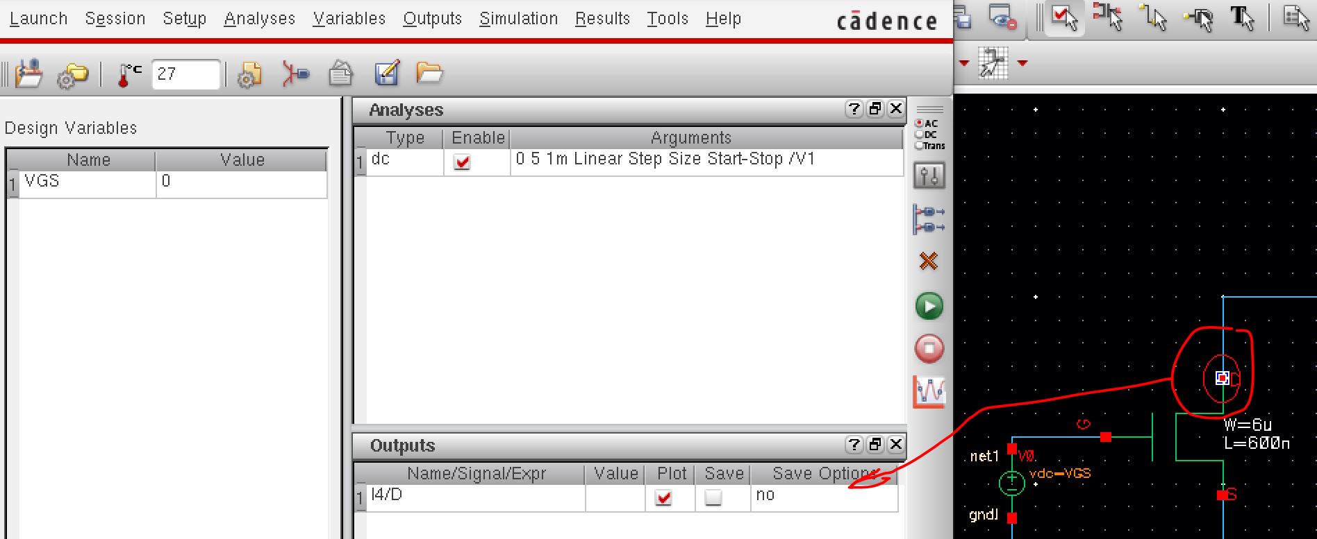
save the state and then in the ADE go to tools and parametic analysis and input the following
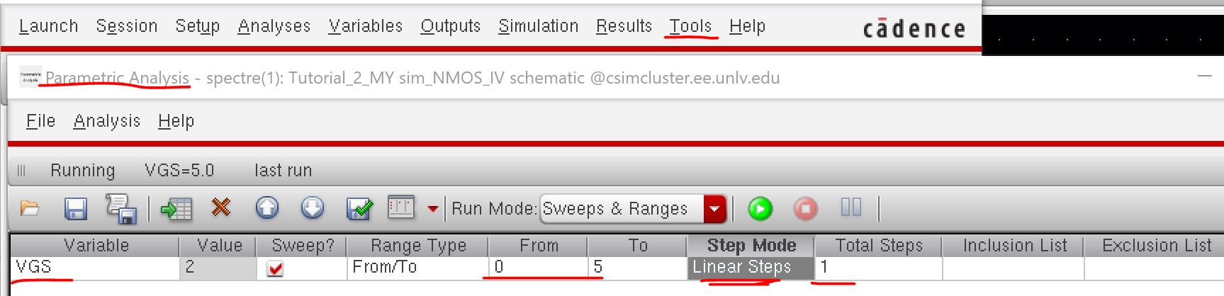
Then run Press the green botton
close
everying and in the library manager creat and new layout. the NMOS is
provied and use the instance to find it and place in the layout. And
add a ptap and add a m1_poly on the top
add metal1 rectangles and place pins and extact when done
next we are going to LVS
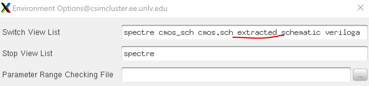
going back the shemcatic go to the Setup-> Environment set the following
then run the Parametric Analysis again
now lets go back and work on the PMOS the same way we did the NMOS
Creat symbol
creat layout and extract
then LVS
creat circuit
Launch the ADE, from scratch, load up the Model Library (Setup -> Model Libraries) and add the following
Going to Analyses -> Choose and Outputs -> To Be Saved -> Select on Schematic, and click on the S pin.
Save this State. Then Tools -> Parametric Analysis, and pressing on Run
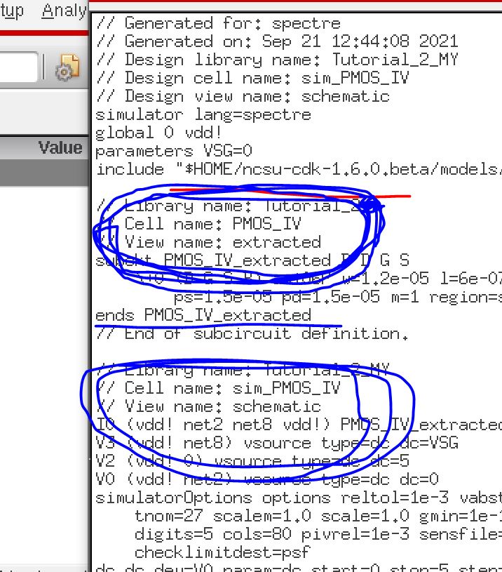
Verifying that the extracted layout is being simmed by going to Simulation -> Netlist -> Display

End of PreLab
*********************************************************************************************************************************************************************
Lab Procedure
- Generate 4 schematics and simulations (see the examples in the Ch6_IC61 library, but note that for the PMOS body should be at vdd! instead of gnd!):
- A schematic for simulating ID
v. VDS of an NMOS device for VGS varying from 0 to 5 V in 1 V steps
while VDS varies from 0 to 5 V in 1 mV steps. Use a 6u/600n
width-to-length ratio.
- A
schematic for simulating ID v. VGS of an NMOS device for VDS = 100 mV
where VGS varies from 0 to 2 V in 1 mV steps. Again use a 6u/600n
width-to-length ratio.
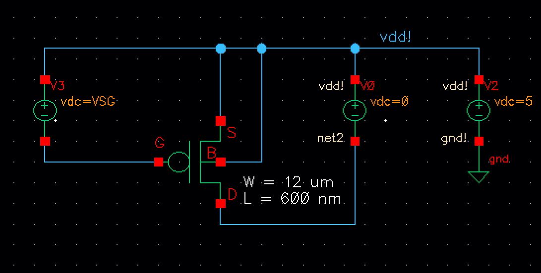
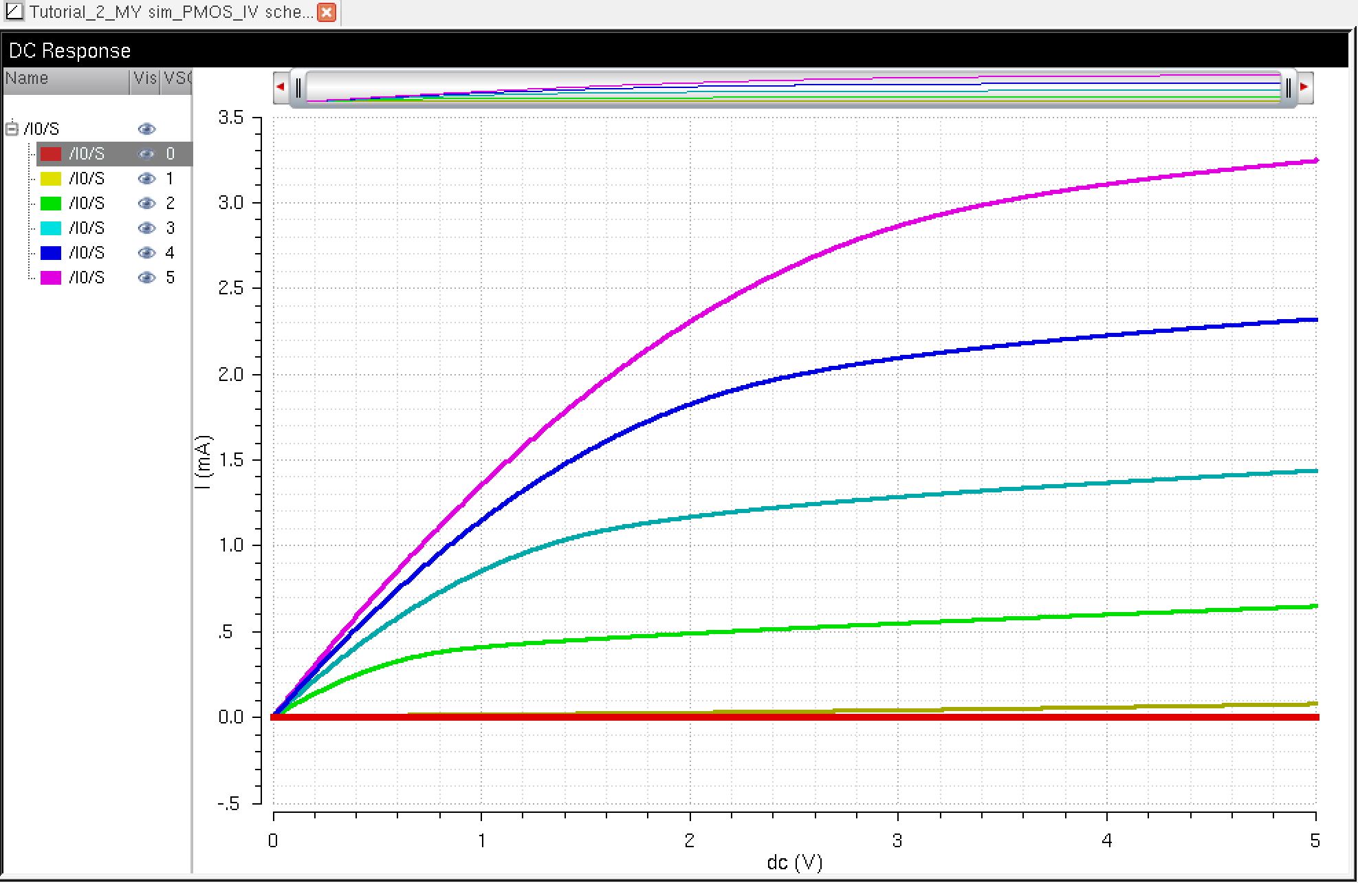
- A
schematic for simulating ID v. VSD (note VSD not VDS) of a PMOS device
for VSG (not VGS) varying from 0 to 5 V in 1 V steps while VSD varies
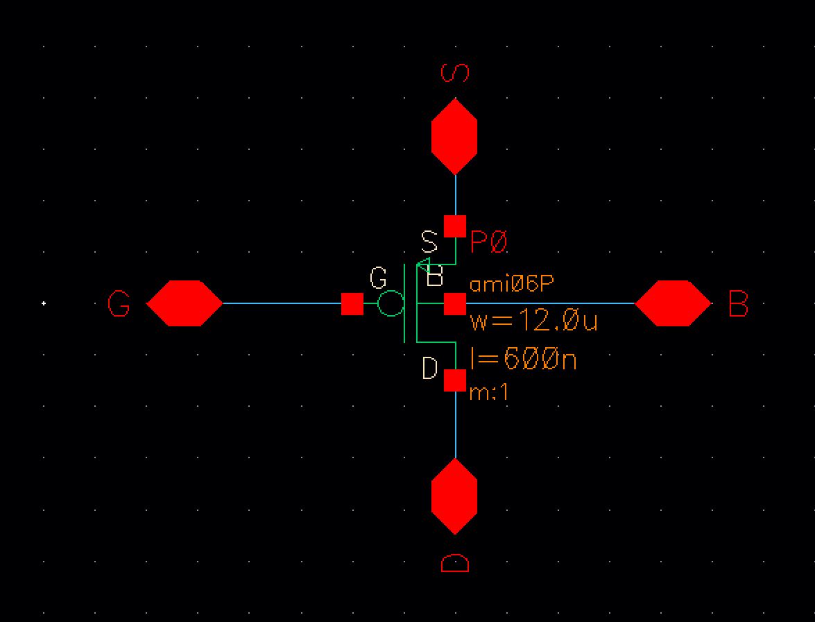
from 0 to 5 V in 1 mV steps. Use a 12u/600n width-to-length ratio.
- A
schematic for simulating ID v. VSG of a PMOS device for VSD = 100 mV
where VSG varies from 0 to 2 V in 1 mV steps. Again, use a 12u/600n
width-to-length ratio.
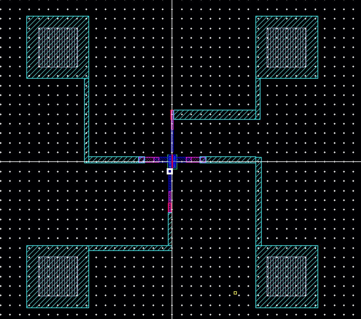
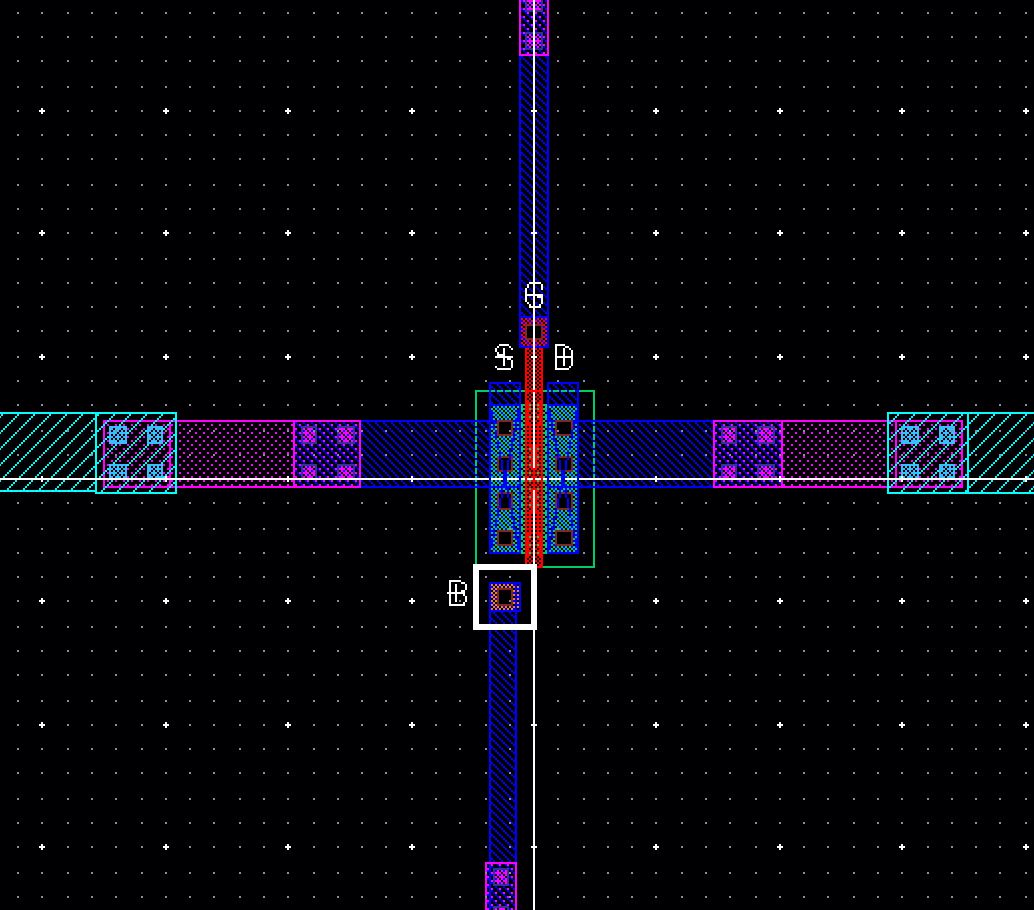
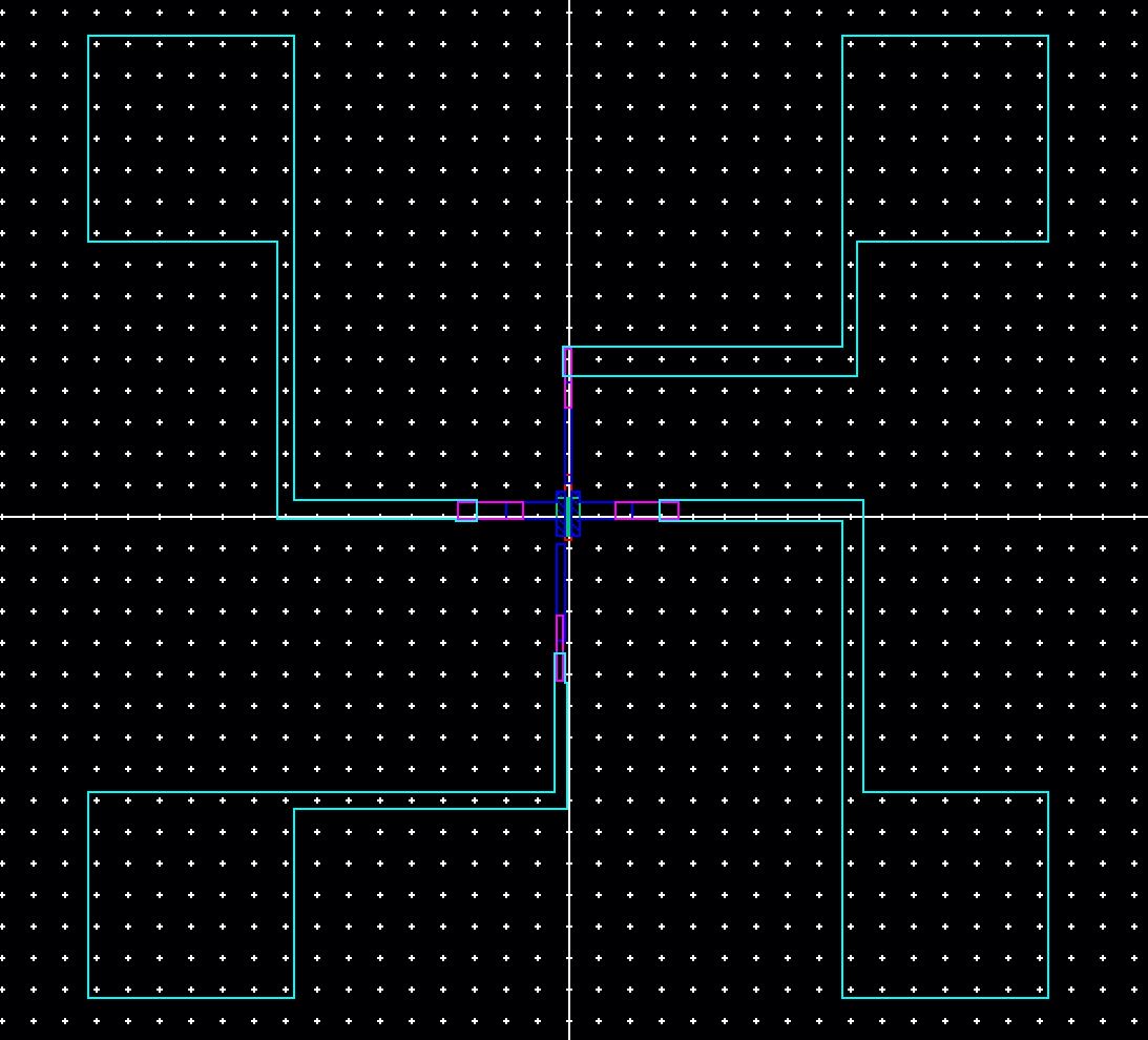
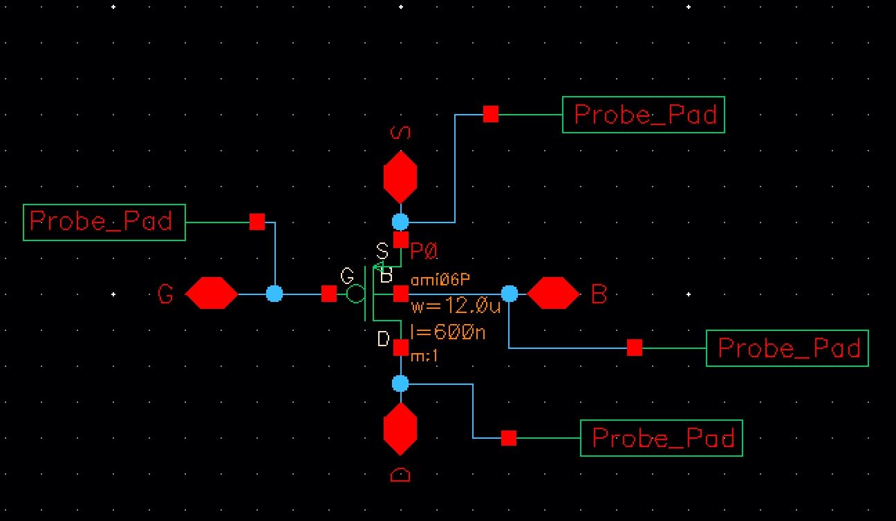
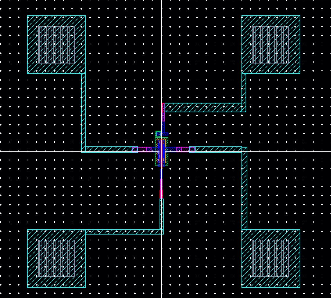
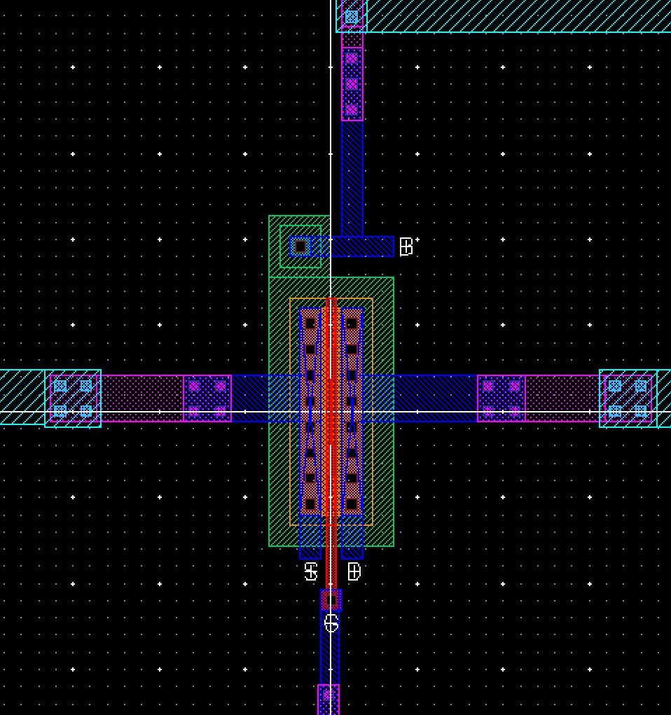
- Lay
out a 6u/0.6u NMOS device and connect all 4 MOSFET terminals to probe
pads (which can be considerably smaller than bond pads [see MOSIS design rules] and directly adjacent to the MOSFET (so the layout is relative small).
- Show your layout passes DRCs.
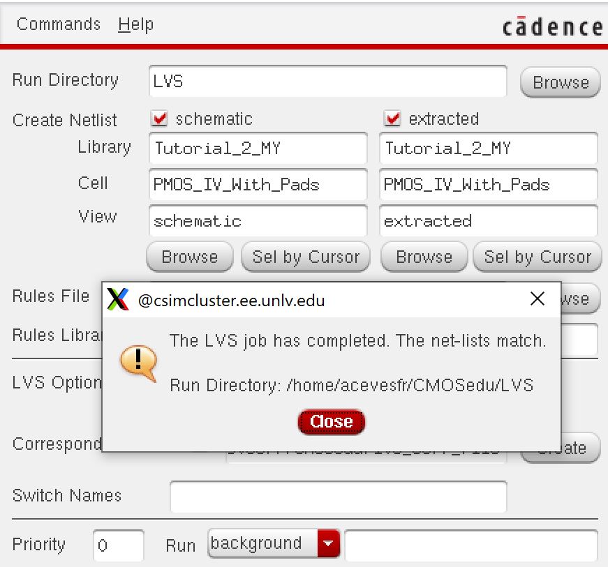
- Make a corresponding schematic so you can LVS your layout.
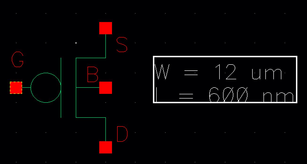
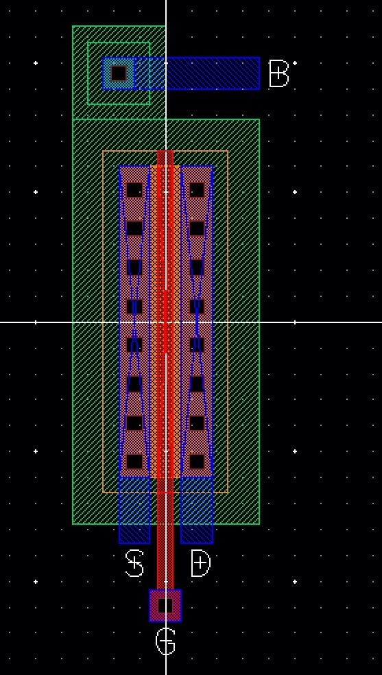
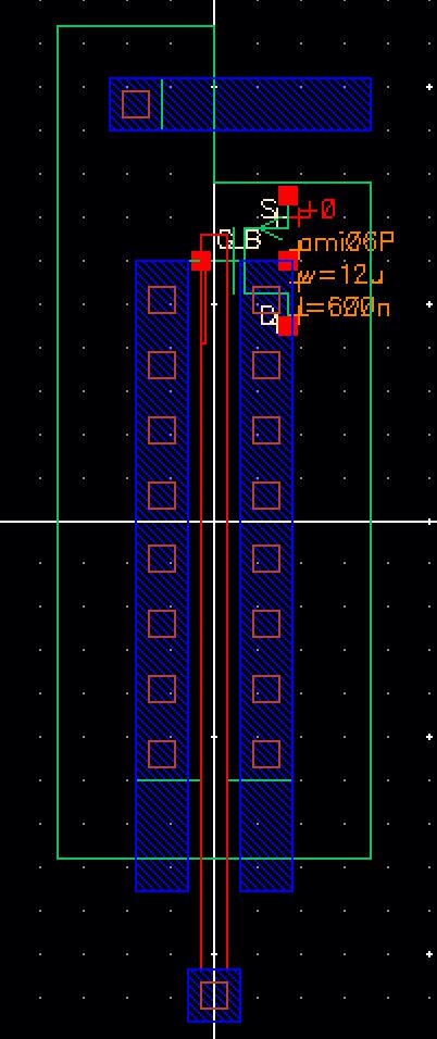
- Lay out a 12u/0.6u PMOS device and connect all 4 MOSFET terminals to probe pads.
- Show your layout passes DRCs.
- Make a corresponding schematic so you can LVS your layout.
- Some examples are seen below (click for a larger view).
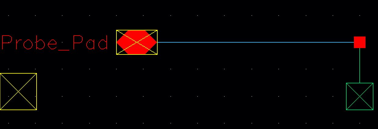
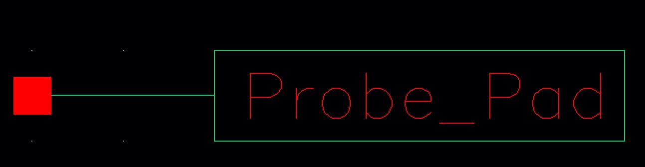
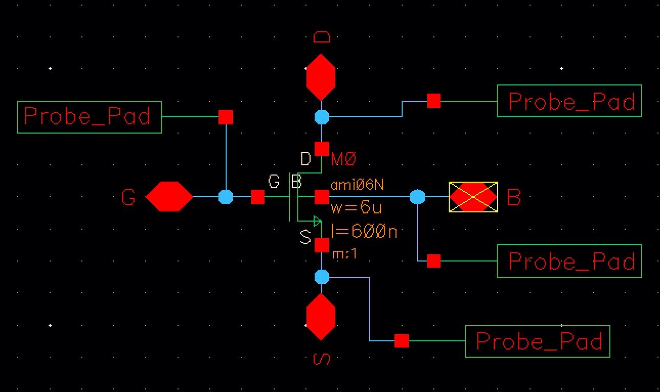
- They
are, in order: 1) probe pad layout, 2) probe pad schematic, 3) probe
pad symbol, 4) schematic of the MOSFET with probe pads, 5)
corresponding symbol view, 6) corresponding layout (which is DRCed and
LVSed), 6) zoomed in view of the layout, and finally 7) simulation
schematic for ID v VSD for varying VSG (which is not used for an LVS
since there is no way to lay out a battery).
- These cells are found in lab4.zip
*************************************************************************************************************************************************************************
Lab Work
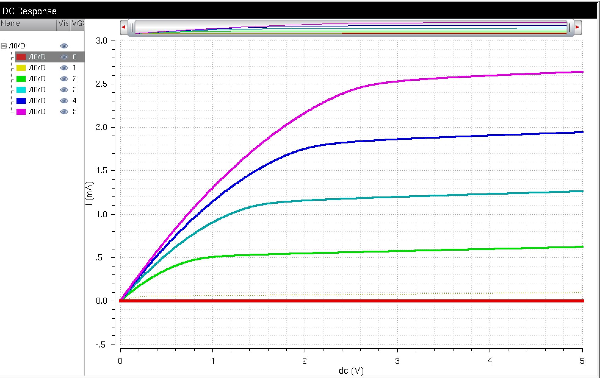
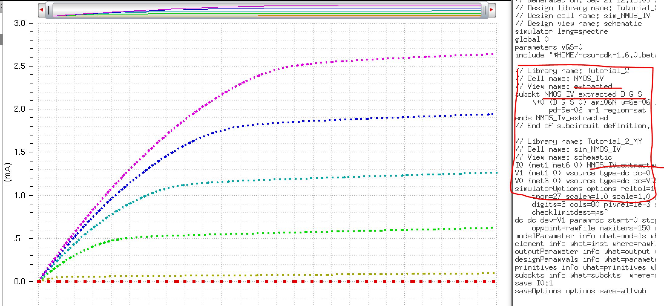
A schematic for simulating ID
v. VDS of an NMOS device for VGS varying from 0 to 5 V in 1 V steps
while VDS varies from 0 to 5 V in 1 mV steps. Use a 6u/600n
width-to-length ratio.
Running the ADE with a DC sweep (Parametric Analysis) (hit same a prelab)
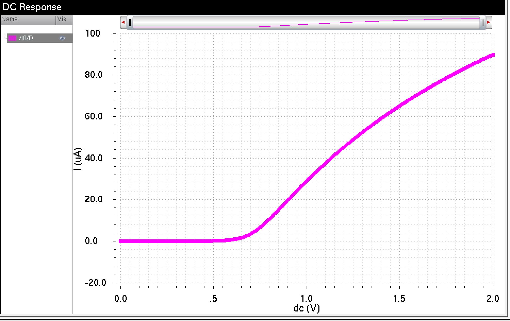
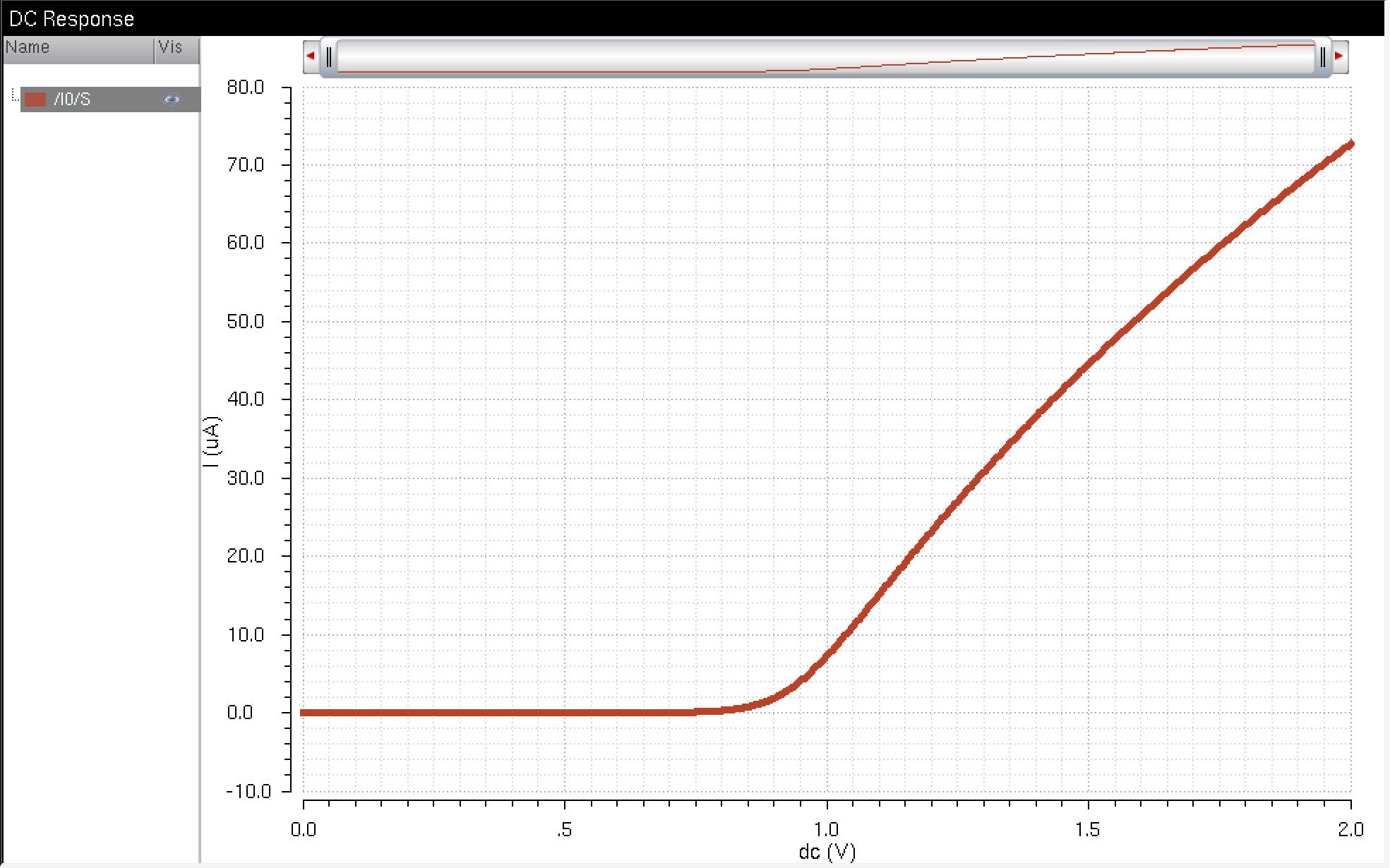
A
schematic for simulating ID v. VGS of an NMOS device for VDS = 100 mV
where VGS varies from 0 to 2 V in 1 mV steps. Again use a 6u/600n
width-to-length ratio.
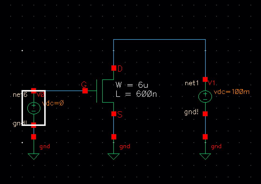
set the following and click on D
A
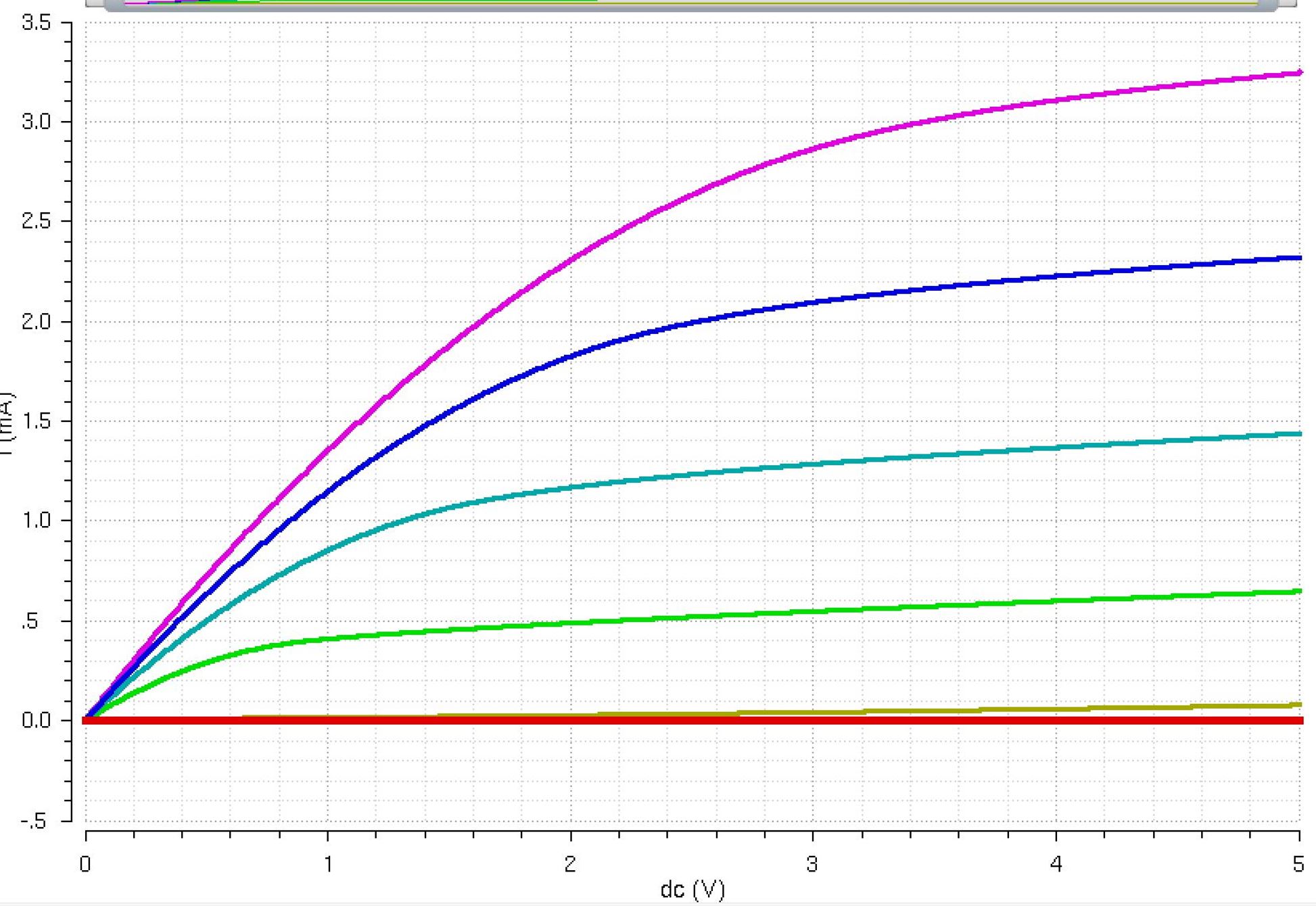
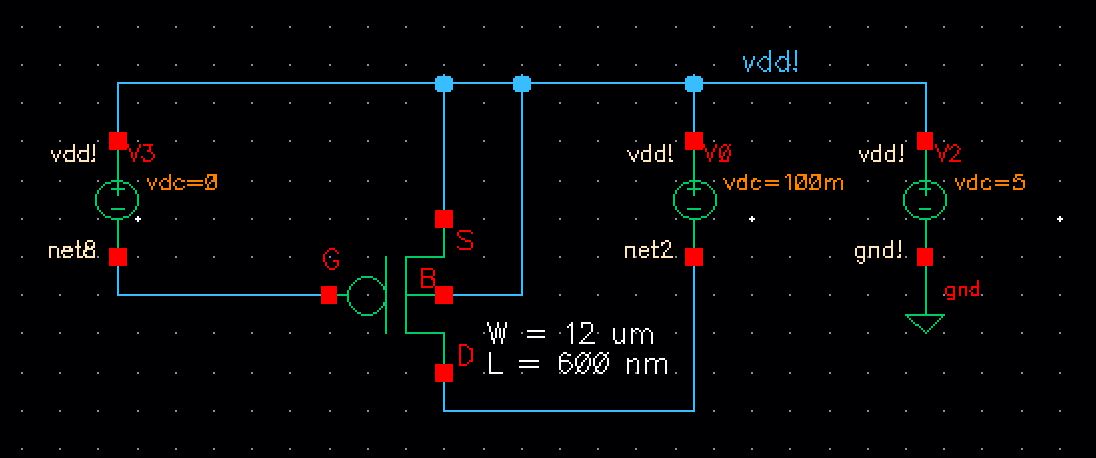
schematic for simulating ID v. VSD (note VSD not VDS) of a PMOS device
for VSG (not VGS) varying from 0 to 5 V in 1 V steps while VSD varies
from 0 to 5 V in 1 mV steps. Use a 12u/600n width-to-length ratio.
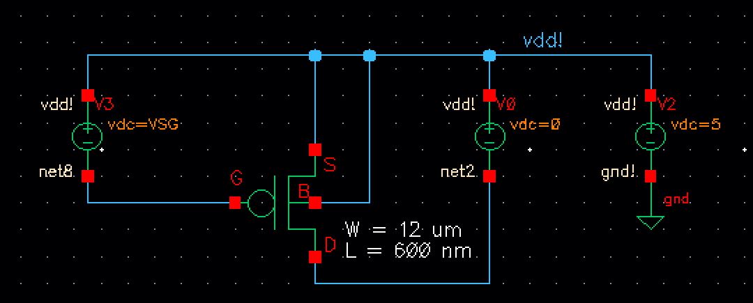
Running the ADE, DC sweep on VSD and Parametric Analysis on VSG
A
schematic for simulating ID v. VSG of a PMOS device for VSD = 100 mV
where VSG varies from 0 to 2 V in 1 mV steps. Again, use a 12u/600n
width-to-length ratio.
set the following in ADE and running
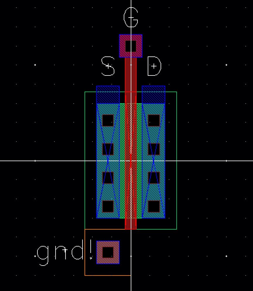
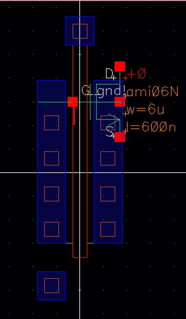
Layout a 6u/0.6u NMOS device and connect all 4 MOSFET terminals to probe
pads
first lets make the pad in layout
Now create a schematic for the probe pad
Create a symbol (Create -> Cellview -> From Cellview)
use symbol in the NMOS schematic
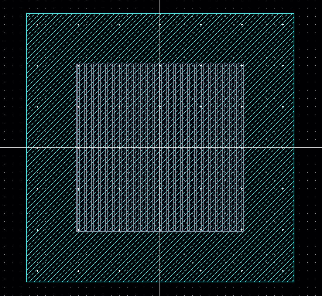
layout the pads with the NMOS while using Metal3 and Metal2 connections, pads are 120u apart by 120u part then DRC
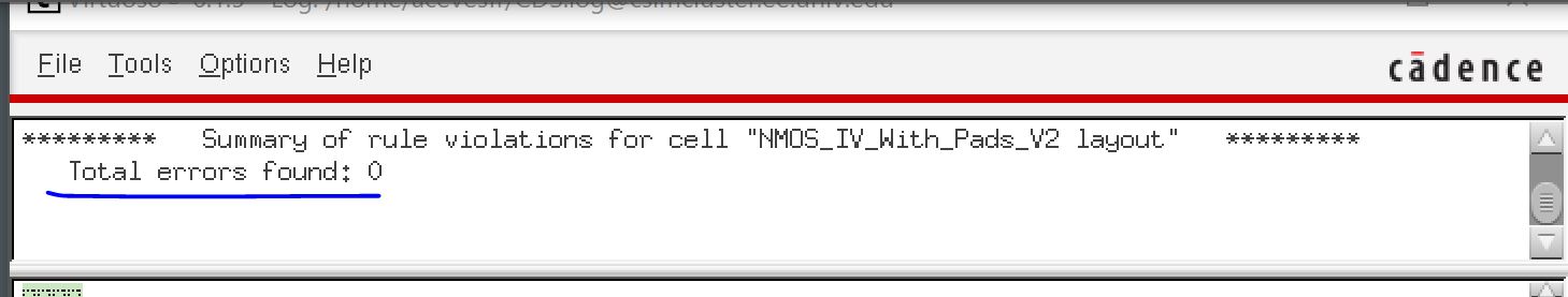
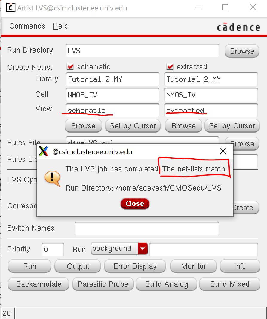
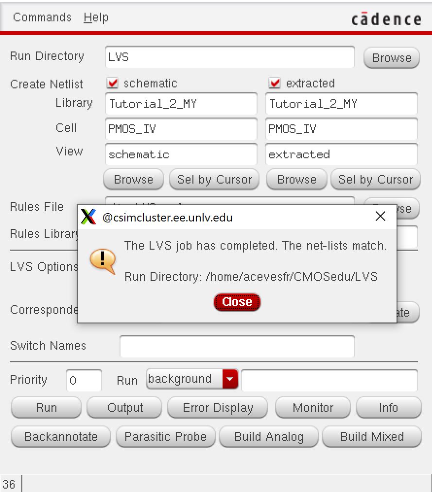
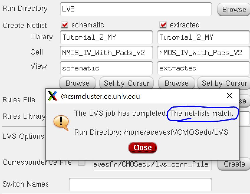
Extract the Layout and LVS
Lay out a 12u/0.6u PMOS device and connect all 4 MOSFET terminals to probe pads.
Next we do the same with the PMOS as we did in NMOS
PMOS layout with pads and extract and DRC
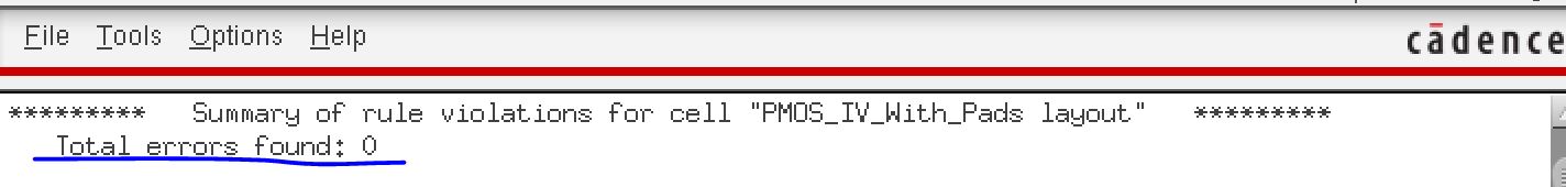
Then LVS
End of Lab
Backup
Return to labs