Lab 6 - EE 421L
Prelab:
- Back-up all of your work from the lab and the course.

- Go through Tutorial 4
- Follow Tutorial 4 and create and layout NAND gate using MOSFETs.


- Read through the lab before starting to work on it.
LAB REPORT:
Experiment 1: Draft the schematic of a 2-input NAND gate using 6u/0.6u MOSFETs and
create layout and symbol views and show the cells DRC and LVS without errors.
Simulate the logical operation of the gates for all 4 possible inputs (00, 01, 10 and 11)
First, draft the schematic and symbol for NAND gate as shown below:
(make the symbol that represents commonly used symbol, and put your initials in the symbol)


Next, layout the 2-input NAND gate (see Tutorial 4) and run DRC and LVS.
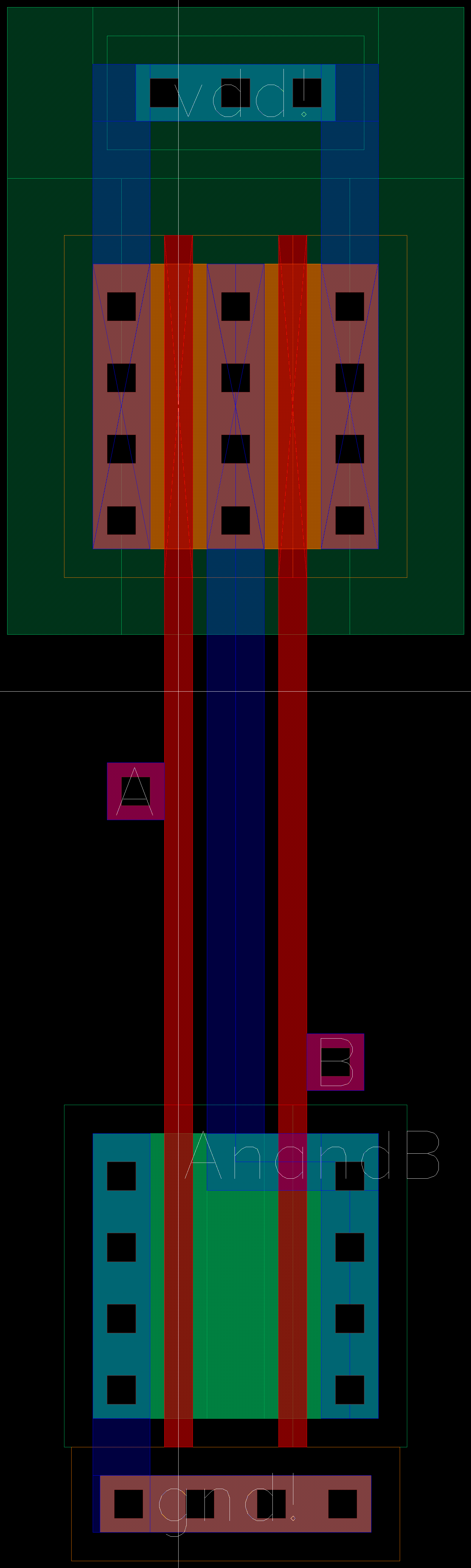
Layout and extracted cell seen below (click for a larger image):
NAND gate cell DRC and LVS without error shown below:


Next, simulate the NAND gate to verify correct logical operation.
Truth table for NAND gate with 2-input is shown below for reference:
| A | B | A nand B |
| 0 | 0 | 1 |
| 0 | 1 | 1 |
| 1 | 0 | 1 |
| 1 | 1 | 0 |
Schematic used for simulation is seen below:

Set up the simulation as seen below:

Simulation plot for 2 input NAND gate shown below:
(0 and 1 represents logical value 'low' or 'high', and numbers shown is generated with graph labels)
* Note: green line represents schematic view and dotted blue line represents extracted view.
* The plot matches with the truth table above and my layout design is verified.
- You can generate this plot by first running the simulation as usual and change the output label to avoid confusion,
then, set the plotting mode to 'Append', go to 'setup' -> 'Environment' and type in 'extracted',
deselect 'A' and 'B' and run simulation again and extracted output should be plotted on the existing plot.

The netlist window below shows that the plot above is simulated with an extracted cell:

Experiment 2: Draft the schematic of a 2-input XOR gate using 6u/0.6u MOSFETs and
create layout and symbol views and show the cells DRC and LVS without errors.
Simulate the logical operation of the gates for all 4 possible inputs (00, 01, 10 and 11)
First, draft the schematic and symbol for XOR gate as seen below:
(make the symbol that represents commonly used symbol, and put your initials in the symbol).
* Note that I used separate inverters (modified version from previous lab) for the XOR gate inputs.


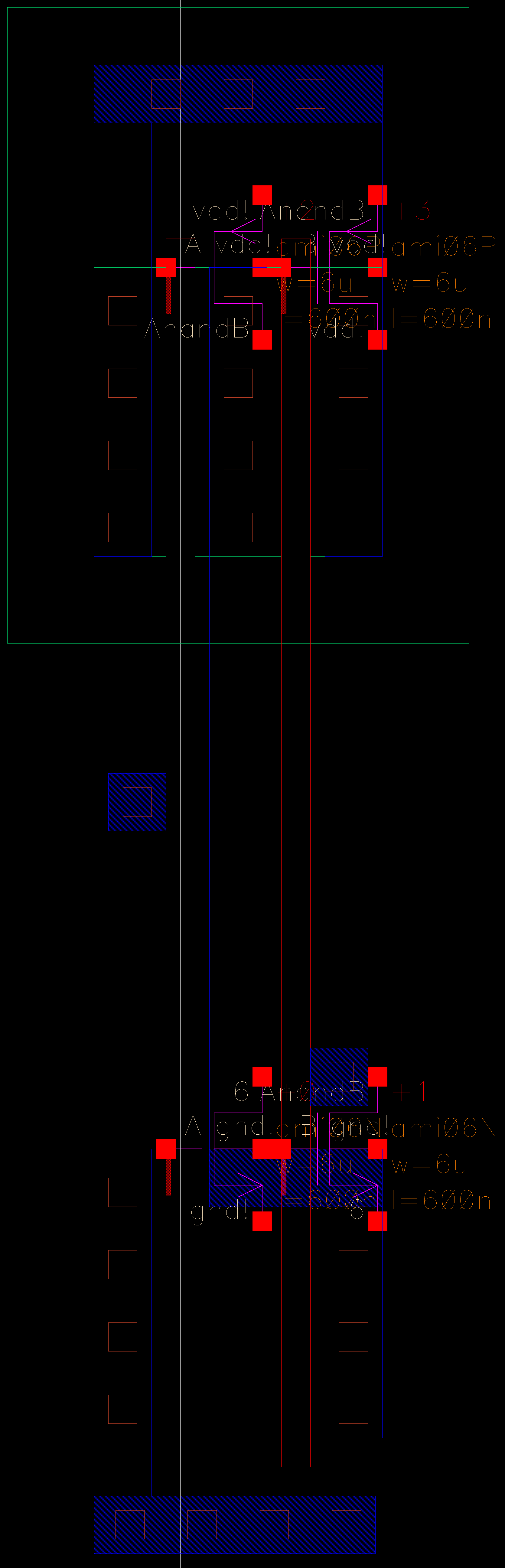
Modified inverters for pin A shown below (layout, schematic & symbol):


Using the inverter layout as a base, layout the XOR gate. Run DRC often to avoid massive number of rule violations.
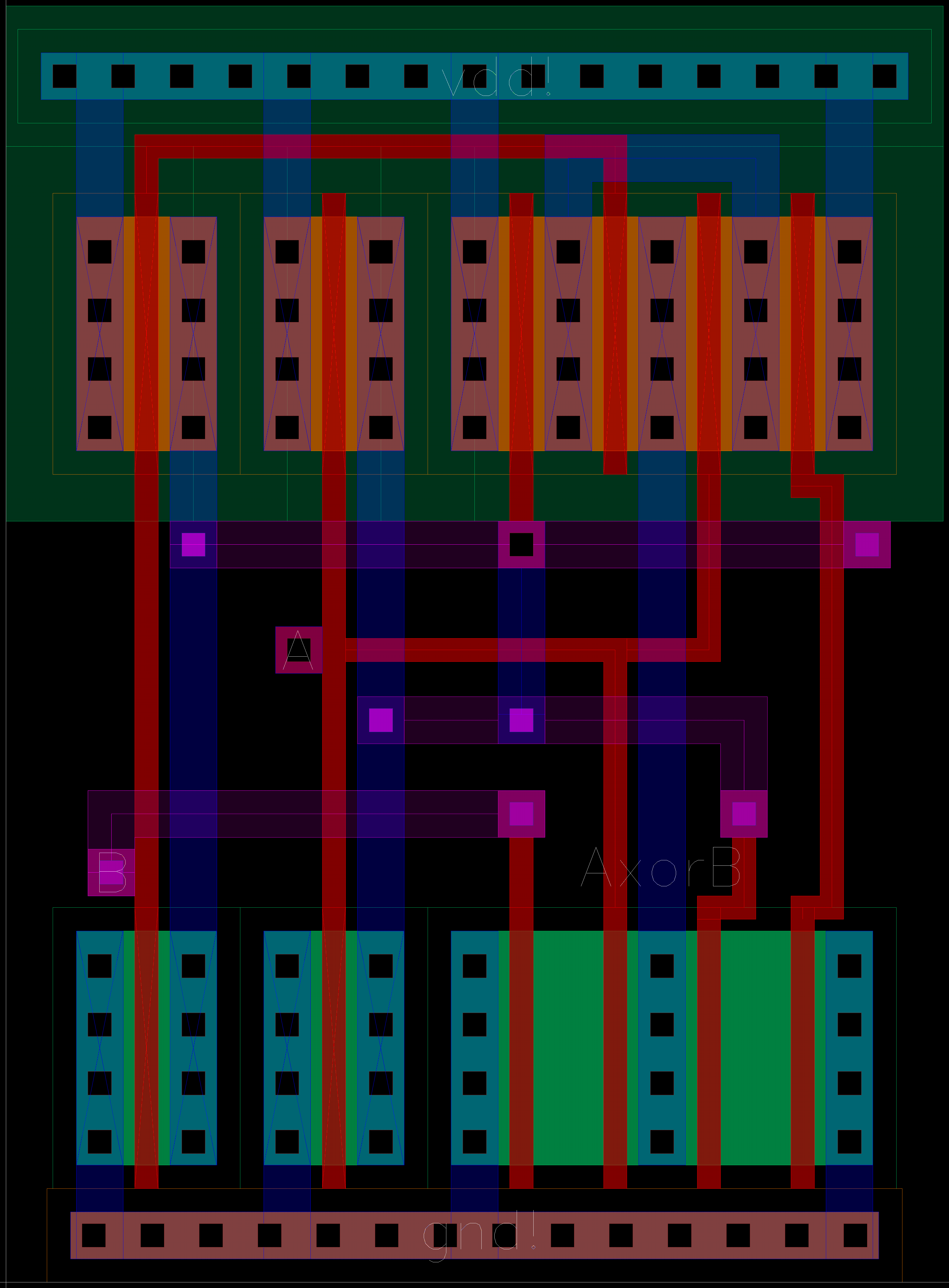
Completed layout and extracted view is shown below (click for a larger image):
- When laying out the cell, use a standard cell height taller than you need to run the metal connections.
- I attempted to make the layout as smallest as possible by stacking select layers next to each other.
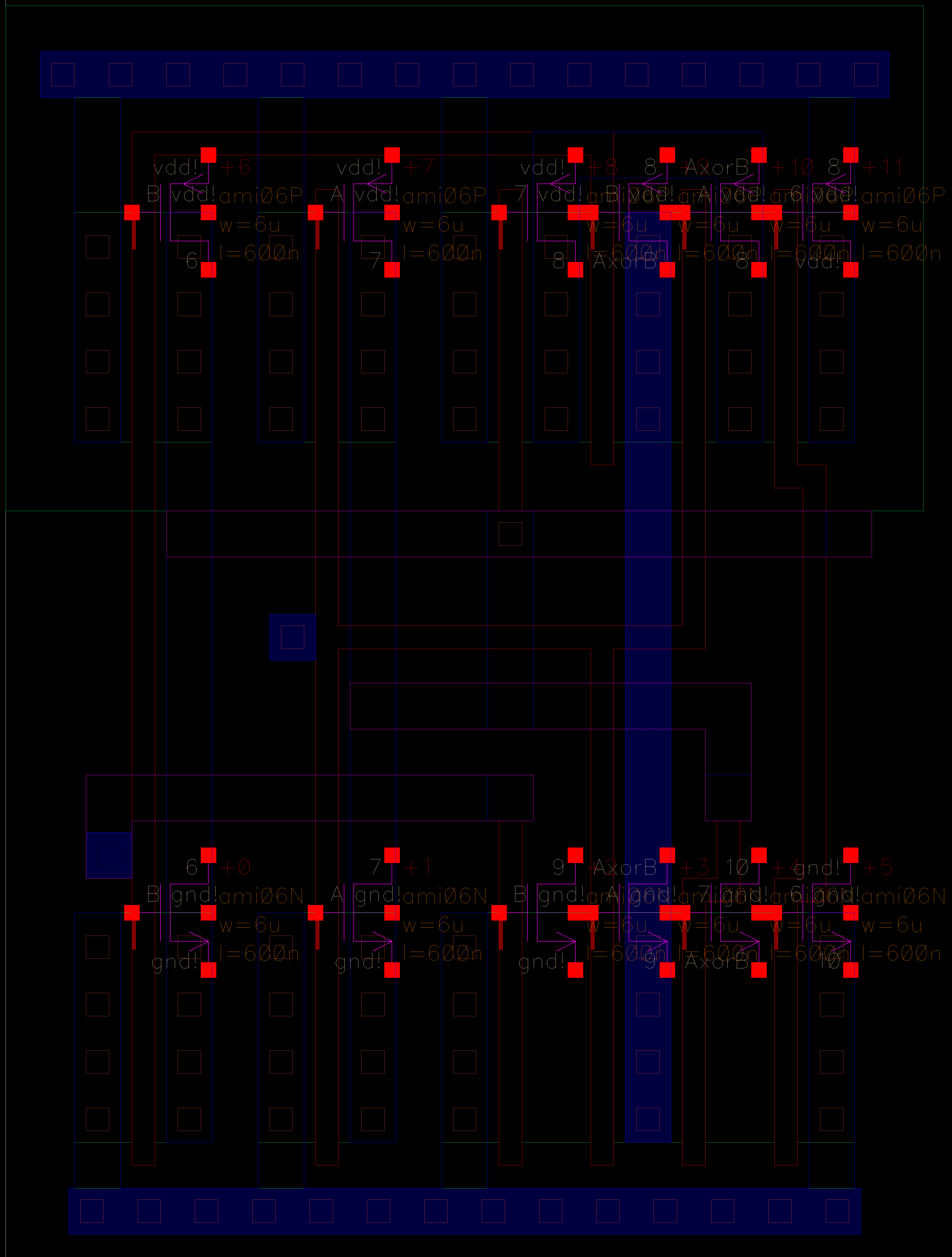
XOR gate cells DRC and LVS without error shown below:


Next, run simulation to verify the correct logical operation of the gate.
Truth table for XOR gate with 2-input is shown below for reference:
| A | B | A xor B |
| 0 | 0 | 0 |
| 0 | 1 | 1 |
| 1 | 0 | 1 |
| 1 | 1 | 0 |
Schematic used for simulation is shown below:

Simulation plot for 2-input XOR gate shown below:
(0 and 1 represents logical value 'low' or 'high', and numbers shown is generated with graph labels)
* Note that light blue represents simulation results from a schematic view and dotted purple line represents extracted view.
* The plot matches with the truth table above and it confirms the layout design is in good working condition.
* Notice the glitch on A xor B output (between 01 input and 10 input), the glitch is caused by the transitional period of voltage turning on and off.
* Timing of the input pulses is not instantaneous in real circuit.
* Input pulses have delays during switching from on & off, causing glitches in the output of a gate (output gets confused for a bit).

The netlist window below shows that plot above is simulated with extracted cell:

Experiment 3: Using the XOR and NAND gate, draft the schematic of a FULL ADDER and
create layout and symbol views and show the cells DRC and LVS without errors.
Simulate the logical operation of the FULL ADDER for all 8 possible inputs (000, 001, 010, 011, 100, 101, 110, 111)
First step is to confirm the good operation of gates by simulating the gates with provided simulation schematic in the lab manual.
Schematic of gate simulation is shown below:

Run simulation using extracted view (see window below)

Simulation plot shown below:

Once you've verified that the logic gates operate correctly,
next step is to create schematic of a FULL ADDER by using the gate symbols created from earlier then create a symbol for a FULL ADDER.
Schematic of a FULL ADDER shown below:

Symbol of a FULL ADDER shown below:

Next step is to simulate the FULL ADDER to verify its operation.
Truth table for FULL ADDER is shown below:
| A | B | Cin | S | Cout |
| 0 | 0 | 0 | 0 | 0 |
| 0 | 0 | 1 | 1 | 0 |
| 0 | 1 | 0 | 1 | 0 |
| 0 | 1 | 1 | 0 | 1 |
| 1 | 0 | 0 | 1 | 0 |
| 1 | 0 | 1 | 0 | 1 |
| 1 | 1 | 0 | 0 | 1 |
| 1 | 1 | 1 | 1 | 1 |
Create a schematic to simulate FULL ADDER (schematic shown below):

Simulation plot shown below:
*Simulated plot matches with the truth table (confirms the correct operation of FULL ADDER).
*Notice that the glitches in the output is due to the imperfect input pulses (slight delays).


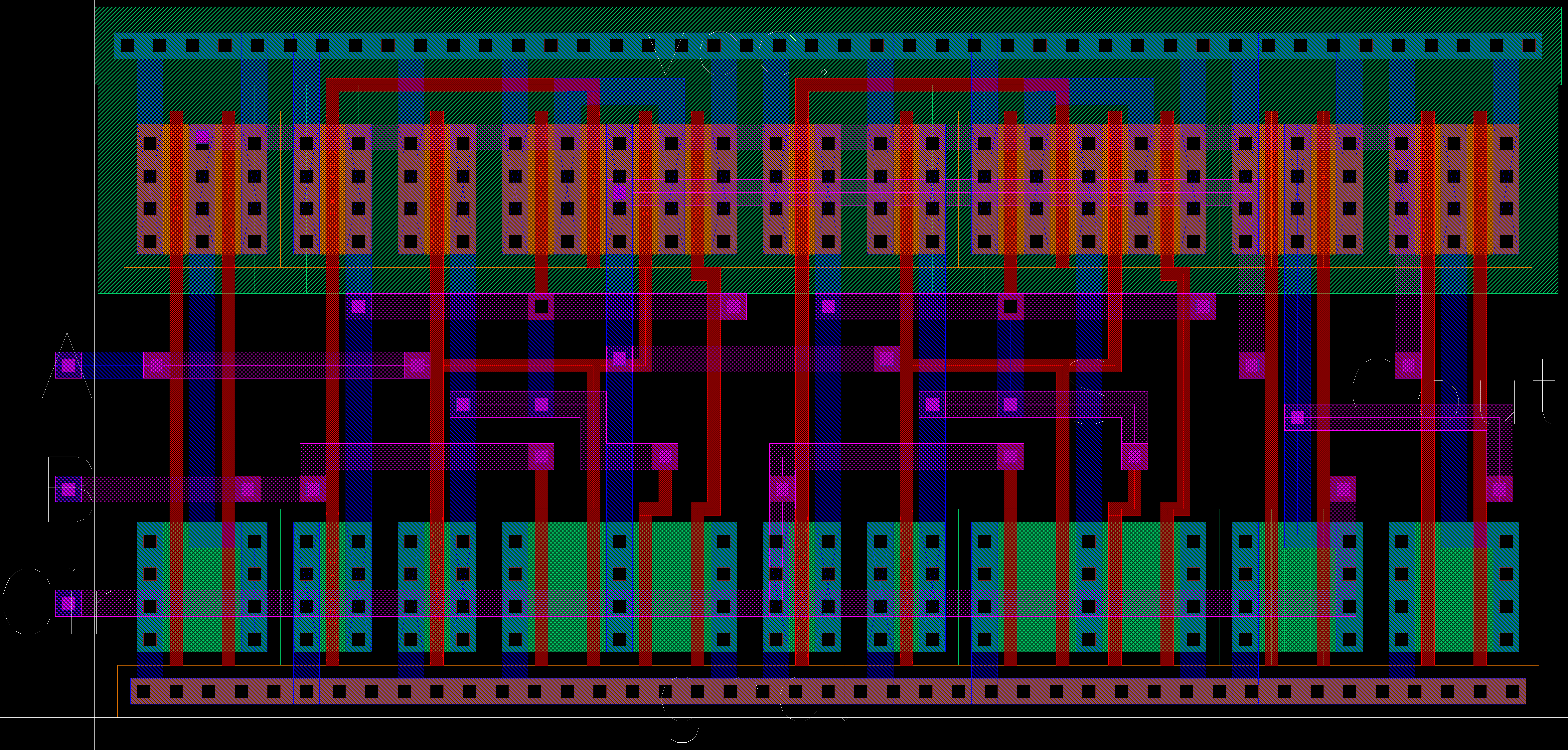
Next step is to layout the FULL ADDER.
- When laying out cell, input and output can be on metal 2, but not metal 3.
- Metal 1 is used for all input and output pins.
- I tried to minimize the layout size by putting select layers next to each other to save space.
- Most of connections made with metal2 and metal 1 using m2_m1 cell.
- vdd! and gnd! is routed with metal 1.
- Layout and extracted view is shown below (click for a larger image):
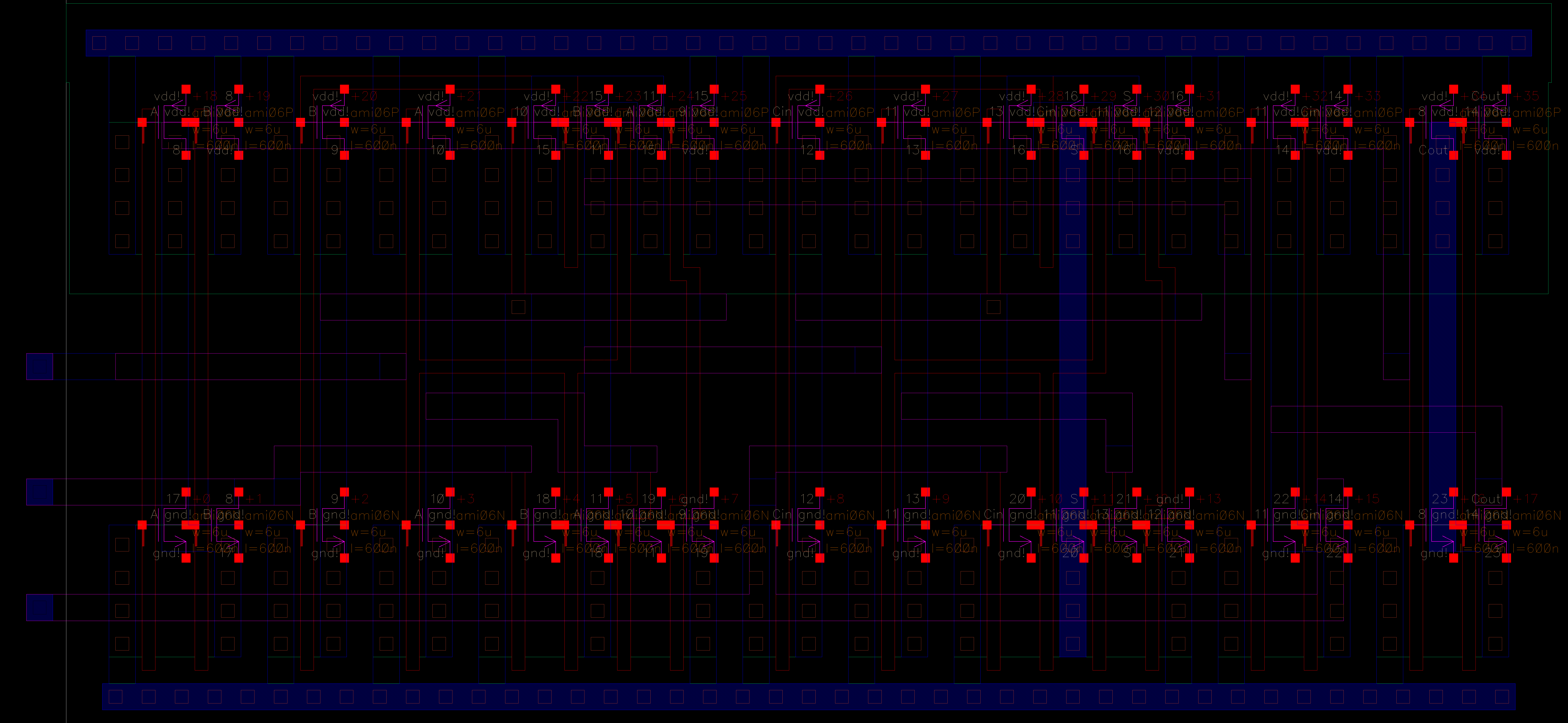
FULL ADDER cells DRC and LVS without error shown below:


Finally, run simulation using extracted view for verification (see below)

Simulation plot shown below:
*dotted lines in 'S' and 'Cout' represent the extracted cell.
*Since the dotted lines didn't diverge from the thick simulated lines, that confirms the layout cell is working properly.

Save & Backup your work
(cells used in this lab is zipped up and saved at index page for future reference)
End of the report