Lab 5 - EE 421L
%%%% Click here to download lab5_pk.zip %%%%
Prelab:
- Back-up all of your work from the lab and the course.
- Go through Tutorial 3 seen here.
layout of an inverter and simulation plot from tutorial 3:
Questions form tutorial 3:
1. What does the Bindkey q do?
2. Which two Cell Views are used when doing an LVS?
3. What is the difference between the nmos and nmos4 schematic cells?
4. How do you select the MOSFET models in the ADE (Analog Design Environment) window?
5. What is the difference between moving and stretching?
6. How do you layout a rectangle on the metal1 layer?
7. What does the ! indicate at the end of gnd! and vdd!
8. What do the acronyms LSW and CIW stand for?
9. How is the ruler used? Cleared?
- press 'k' for ruler, shift + 'k' for clear ruler.
Lab Report:
- Draft schematics, layouts, and symbols for two inverters having sizes of:
- 12u/6u (= width of the PMOS/ width of the NMOS with having minimum length of 600n)
- Follow the tutorial and create schematic and symbol for 12u/6u inverter as seen below:


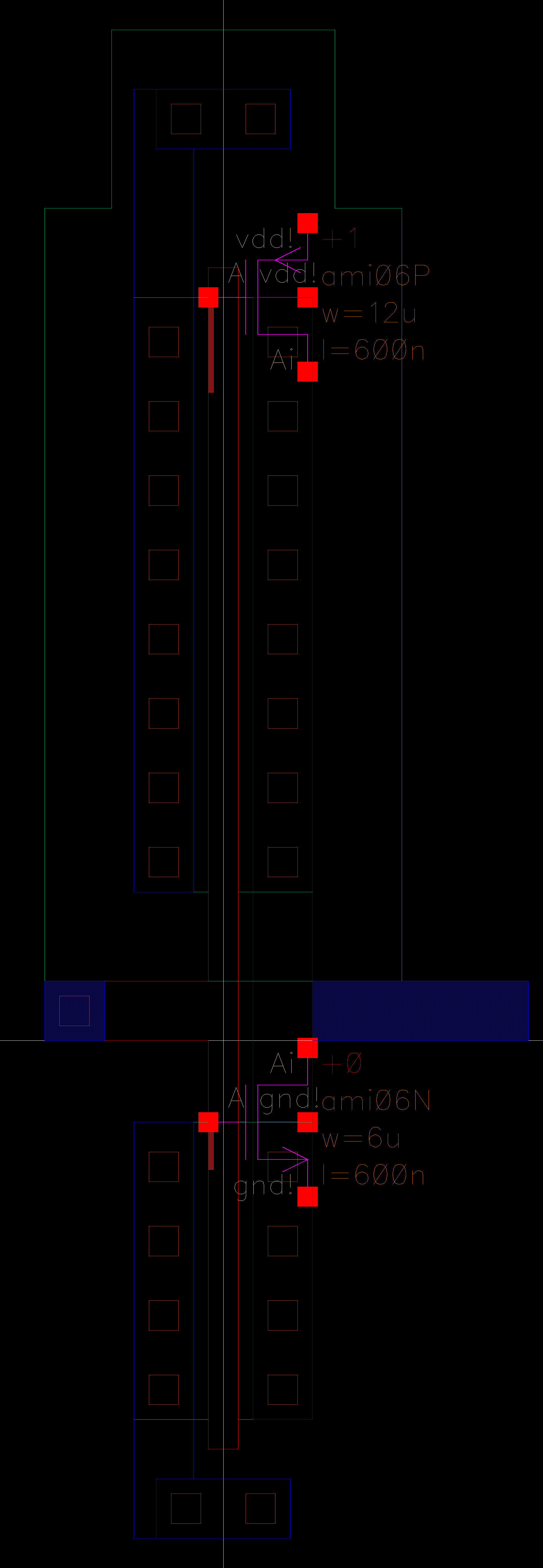
- Layout the 12u/6u inverter as seen below:
(click on the image to view the layout in full detail) (extracted view of the inverter)
- Run DRC for errors and Run LVS:
- Draft schematics, layouts, and symbols for two inverters having sizes of:
- 48u/24u where the devices use a multiplier, M = 4
- Draft schematic and symbol of the inverter


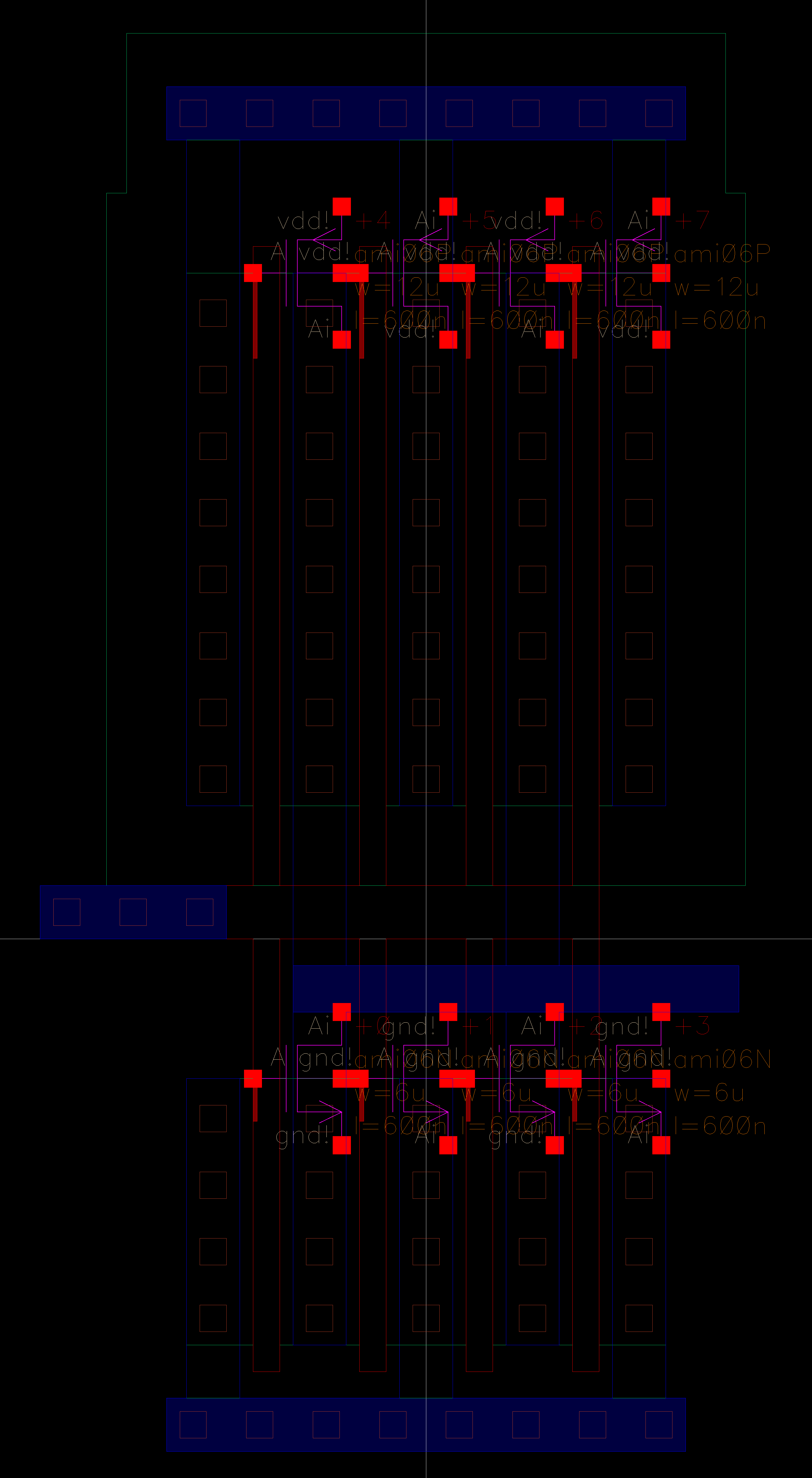
- Layout the 48u/24u inverter as seen below:
(click on the image to view the layout in full detail) (extracted view of the inverter)
- Run DRC for errors and Run LVS:
- Using SPICE simulate the operation of both of your inverters showing each driving a 100fF, 1pF, 10pF, and 100pF capacitive load
- Create a schematic to run simulations for 12u/6u inverter:
(note that capacitor value is not defined, instead of running 4 separate simulations, use paramatric analysis to run 4 simulations at once)

- Launch ADE-L and setup the simulation as seen below:
- Run simulation with extracted cell for verification:
- Simulation Results: (note that label was created by using random marker and changing name for appearance)
- From the plot below, small capacitor (100fF & 1pF) load is inverted,
but as capacitor value increases (10pF & 100pF) output isn't inverted due to delay of the capacitor.

- Use UltraSim and repeat the above simulations:
- Set-up simulation as above, note that UltraSim only performs transient simulations:
- Run simulation with extracted cell for verification:
- Simulation Results: (note that label was created by using random marker and changing name for appearance)
- The UltraSim plot is the same as Spectre plot. (UltraSim is less accurate compared to Spectre)

- Using SPICE simulate the operation of both of your inverters showing each driving a 100fF, 1pF, 10pF, and 100pF capacitive load
- Create a schematic to run simulations for 48u/24u inverter: (follow the same procedure as above)

- SPECTRE Simulation Results of 48u/24u inverter:

- UltraSim Simulation Results of 48u/24u inverter: (same as Spectre plot)

- Side by side comparison between 12u/6u inverter & 48u/24u inverter plot:
- Increased in the width of mosfet improved the performance of the inverter,
because wider mosfet allowed more current to flow between drain and source.


- Zip up these cells in a directory call lab5_pk.zip and link to your lab report.
%%%% Click here to download lab5_pk.zip %%%%


