
Lab 8 - EE 421L Fall 2020
The test structures of the chip should include the following:
- one, or more if possible, course projects.
- A 31-stage ring oscillator with a buffer for driving a 20 pF off-chip load.
- NAND and NOR gates using 6/0.6 NMOSs and 12/0.6 PMOSs.
- An inverter made with 6/0.6 NMOS and a 12/0.6 PMOS/
- Transistors, both PMOS and NMOS, measuring 6u/0.6u
where all 4 terminals of each device are connected to bond pads.
- A 25K resistor, and use the 25K resistor and a 10K resistor to implement a voltage divider.
Each test circuit should have its own power but ground should be shared between thhe circuits.
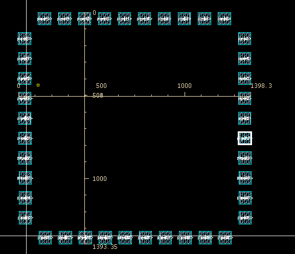
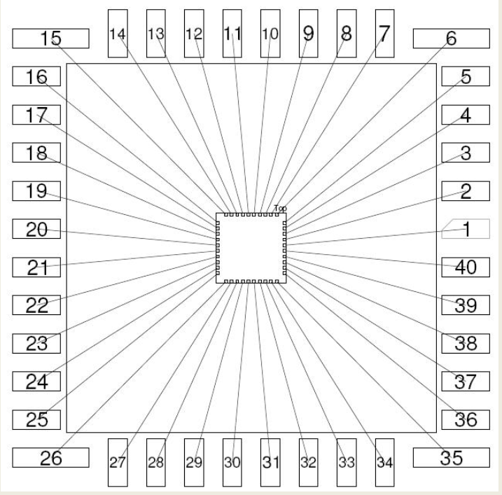
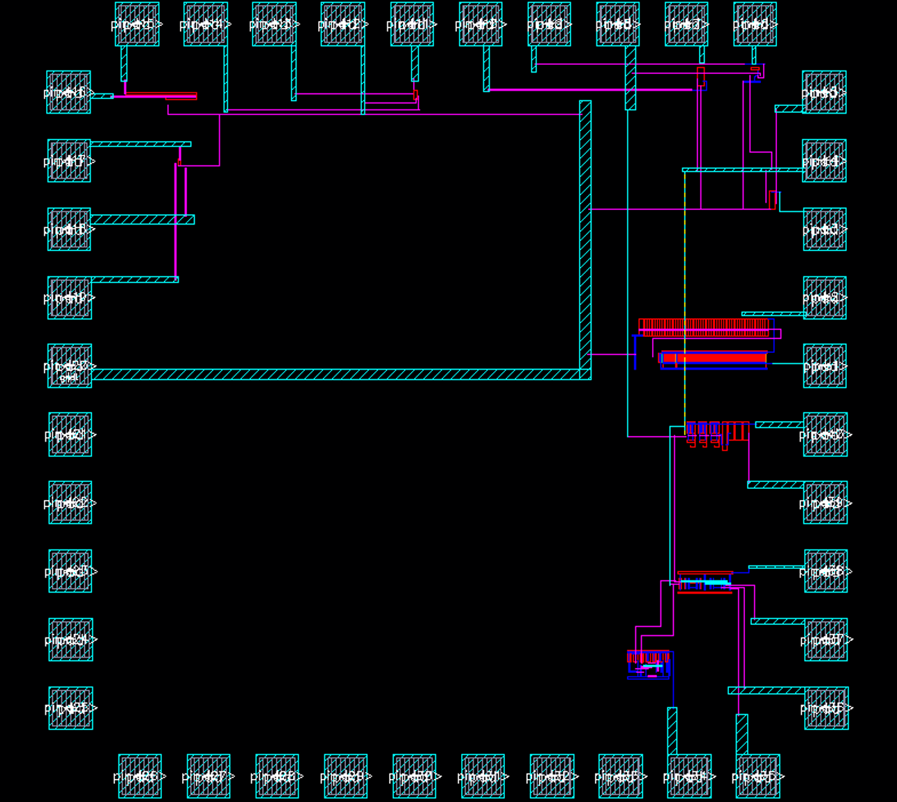
Chip's pads correspond to the 40 pins is seen below:
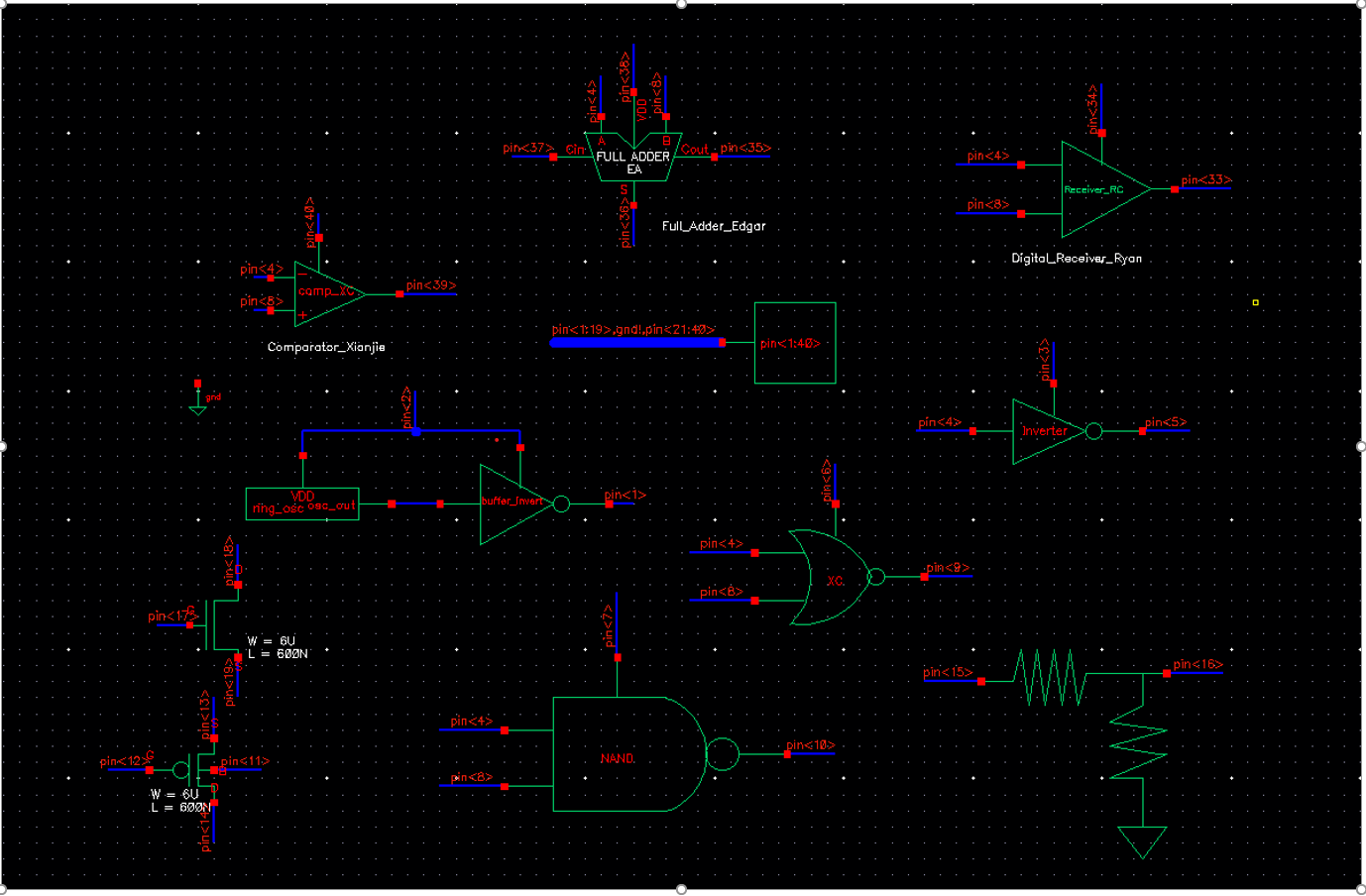
Chip schematic:
Lab procedures:
1) Course Projects
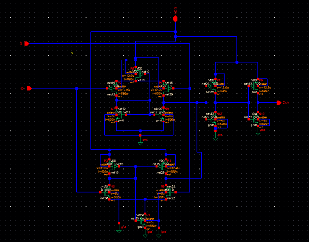
- Ryan's Digital Receiver:
schematic:
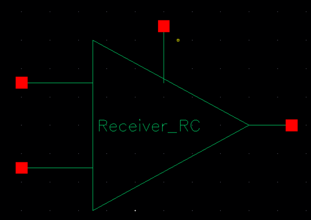
Symbol:
Layout:
input: pin<4> and pin<8>.
output: pin<33>.
VDD: pin<34>.
GND: pin<20> (Shared ground).
To test the digital receiver of the chip simply just provide the VDD to pin<34> then connect a differential pair of input to the pin<4> and pin<8>, then the output will be produced at pin<33>.
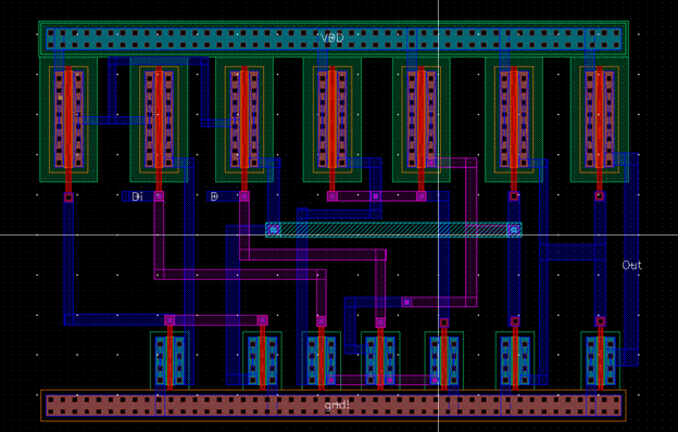
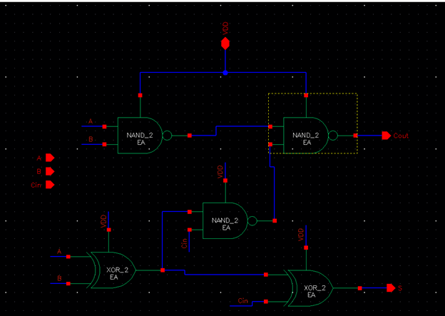
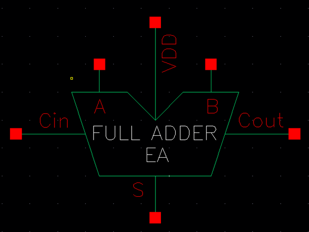
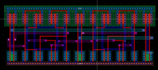
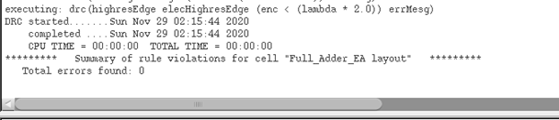
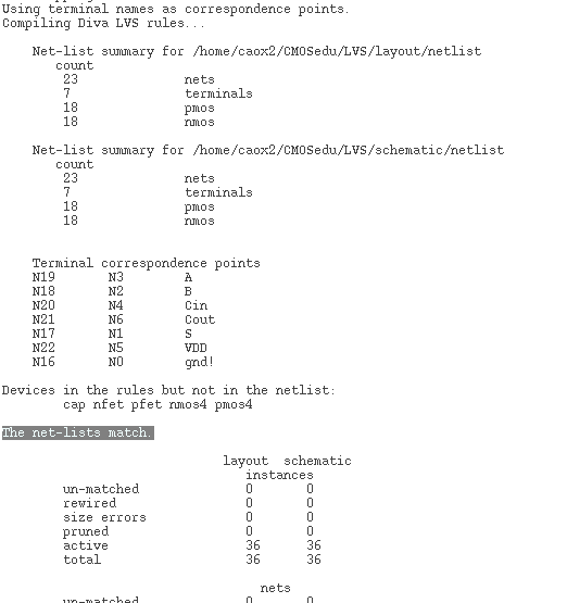
- Edgar's Full Adder
schematic:
Symbol:
Layout:
Input: pin<4>, Pin<8> and pin<37>(Cin).
output: pin<36>(S) and pin<35>(Cout).
VDD: pin<38>.Schematic:
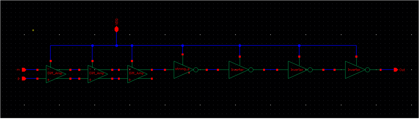
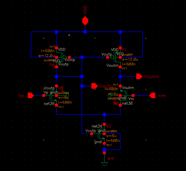
Schematic for the differential amplifier:
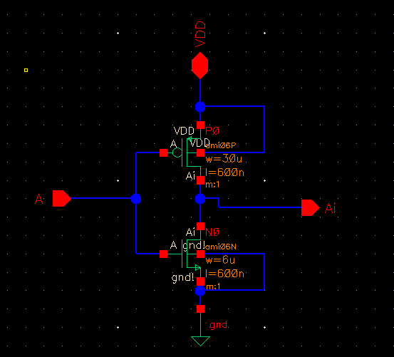
schematic for the strong_p inverter:
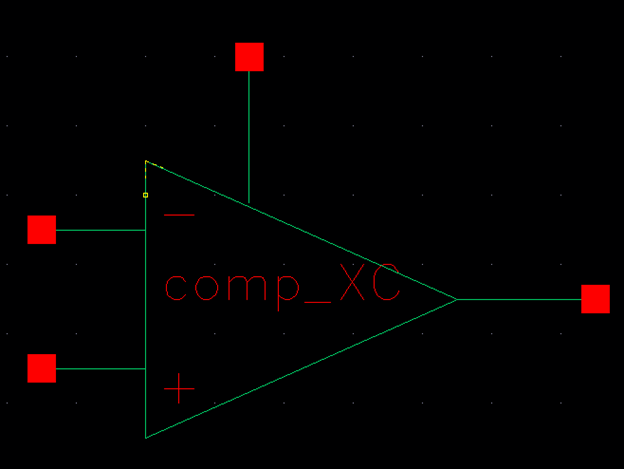
Symbol for the comparator:
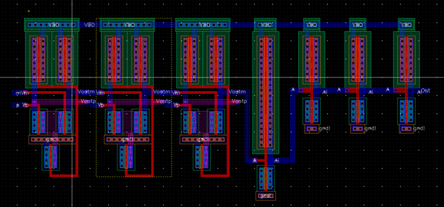
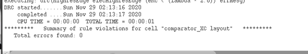
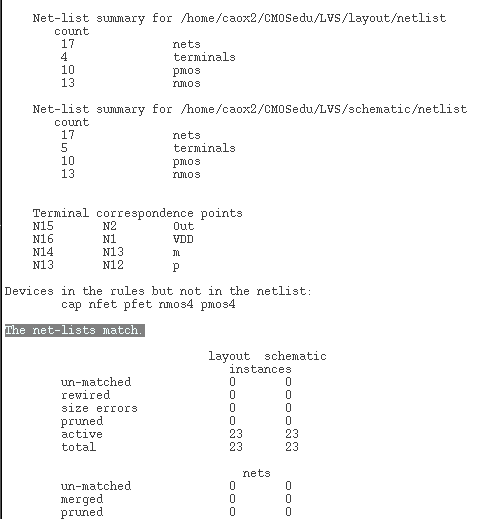
Layout:
Input: pin<4> and pin<8>.
Output: pin<39>.
VDD: pin<40>.
GND: pin<20> (Shared ground).
To test the comparator of the chip simply provide VDD to pin<40> then inputs to the pin<4> and pin<8>, output will be generated at pin<39>.
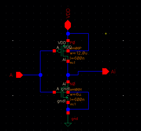
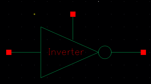
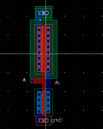
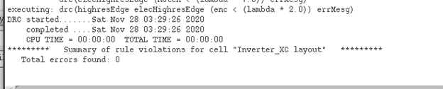
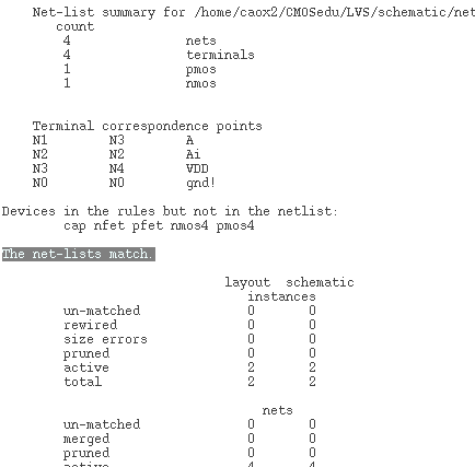
2) An inverter made with a 6/0.6 NMOS and a 12/0.6 PMOS.
Schematic:
Symbol:
Layout:
Input: pin<4>
output: pin<5>
VDD: pin<3>
GND: pin<20> (shared ground)
To test the inverter of the chip, simply just provide VDD to pin<3> and input to thhe pin<4>, output will be generated at pin<5>.
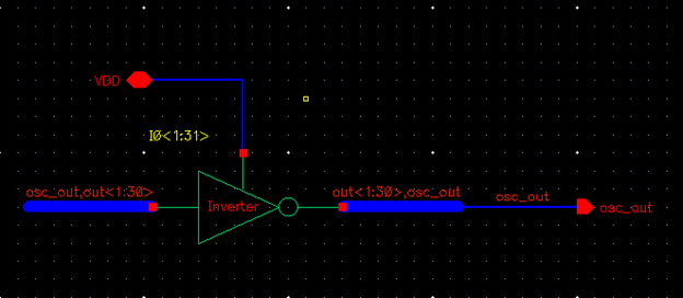
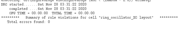
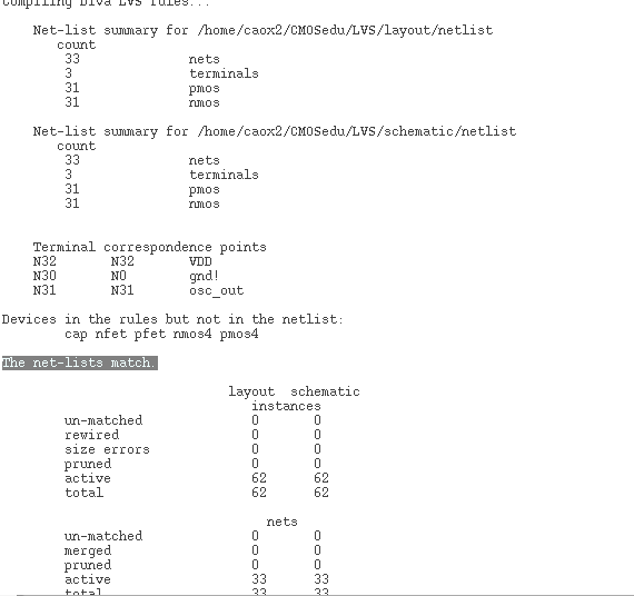
3) A 31-stage ring oscillator with a buffer for driving a 20 pF off-chip load.
Schematic of the ring oscillator:
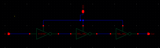
Schematic of the buffer:
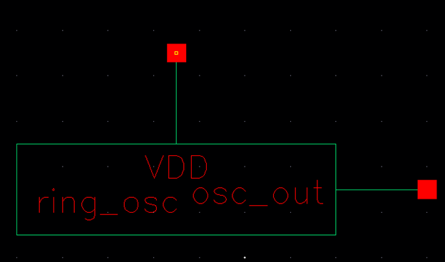
Symbol of the ring oscillator:
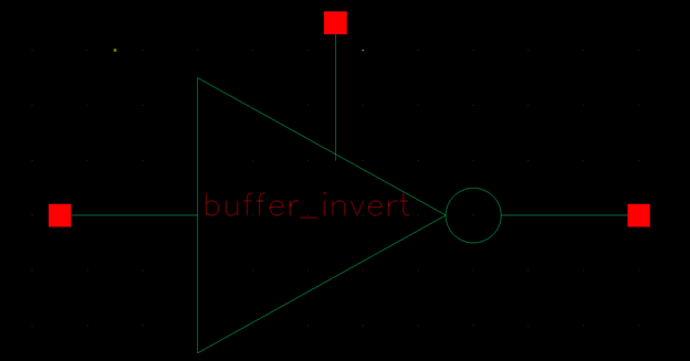
Symbolf of the buffer:
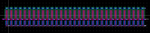
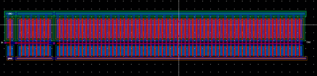
Layout of the ring oscillator:
Layout of the buffer:
Input: N/A
output: pin<1>
VDD: pin<2>
GND: pin<20>
To test the ring oscillator of the chip, just supply VDD to the pin<2> then output should be produced at pin<1>.
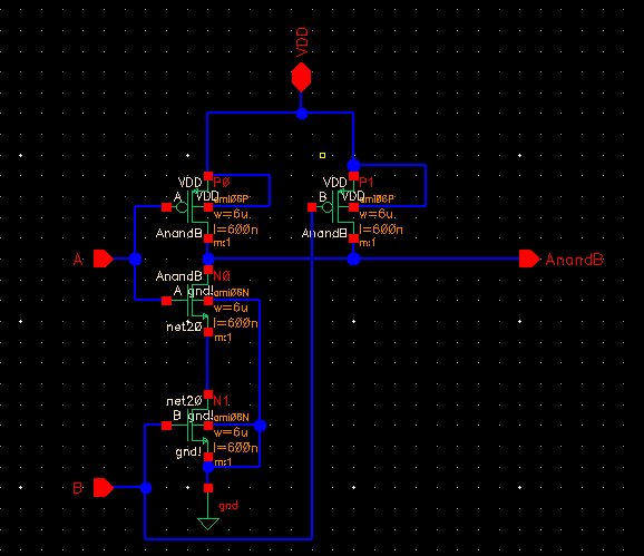
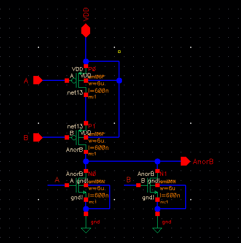
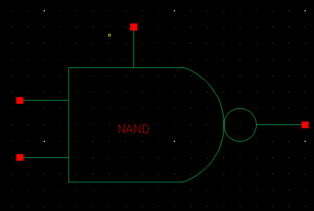
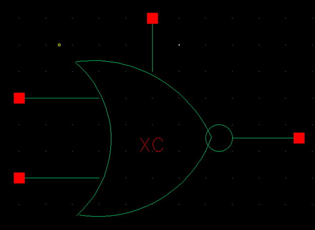
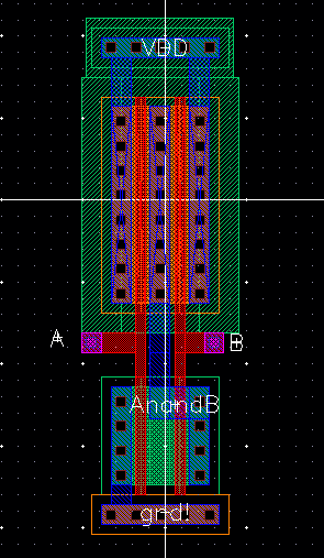
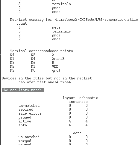
4) NAND and NOR gates using 6/0.6 NMOSs and 12/0.6 PMOSs.
Schematic of the NAND gate:
Schematic of the NOR gate:
Symbol of the NAND:
Symbol of the NOR:
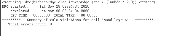
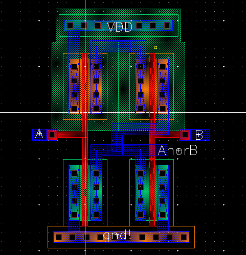
Layout of the NAND:
Layout of the NOR:

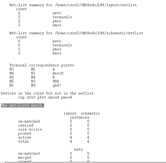
Inputs of the NAND: pin<4> and pin<8>
output of the NAND: pin<10>
VDD: pin<7>
GND: pin<20> (shared ground).
Inputs of the NOR: pin<4> and pin<8>
output of the NOR: pin<9>
VDD: pin<6>
GND: pin<20> (shared ground).
To test the NAND and the NOR, simply provide VDD to pin<7> and pin<6>, then inputs on pin<4> and pin<8>, then output of the NAND will be generated on pin<10>, pin<9> for the NOR.
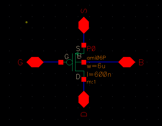
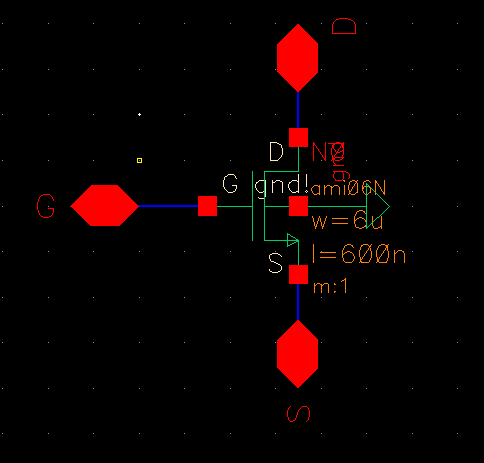
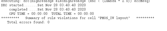
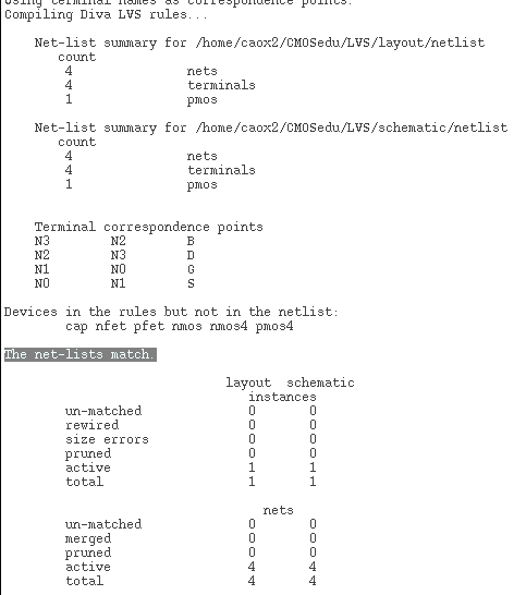
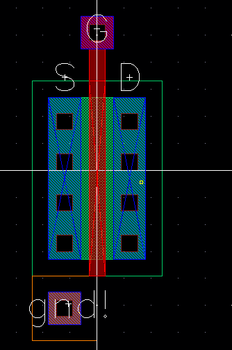
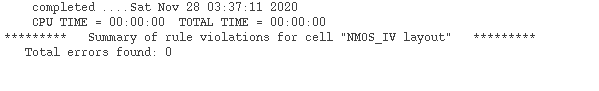
5) Transistors, both PMOS and NMOS, measuring 6u/0.6u where all 4 terminals of each device are connected to bond pads.
Schematic of the PMOS:
Schematic of the NMOS:
Symbol of the PMOS:
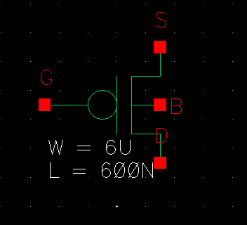
Symbol of the NMOS:
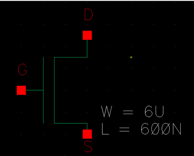
Layout of the PMOS:
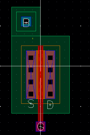
Layout of the NMOS:
Gate of the PMOS: pin<12>.
Drain of the PMOS: pin<14>.
Source of the PMOS: pin<13>.
Body of the PMOS: pin<11>.
Gate of the NMOS: pin<17>.
Drain of the NMOS: pin<18>.
Source of the NMOS: pin<19>.
Body of the NMOS: pin<20>(shared ground).
To test the PMOS, just apply gate voltage to pin<12>, then the drain voltage to pin<14>, then source voltage to pin<13>, and lastly, body voltage to pin<11>.
To test the NMOS, just apply gate voltage to pin<17>, then the source voltage to pin<19>, then drain voltage to pin<18>, and lastly, body to GND (pin<20>).
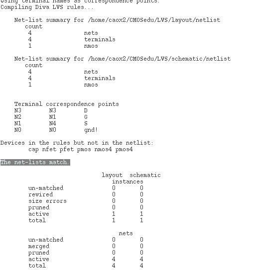
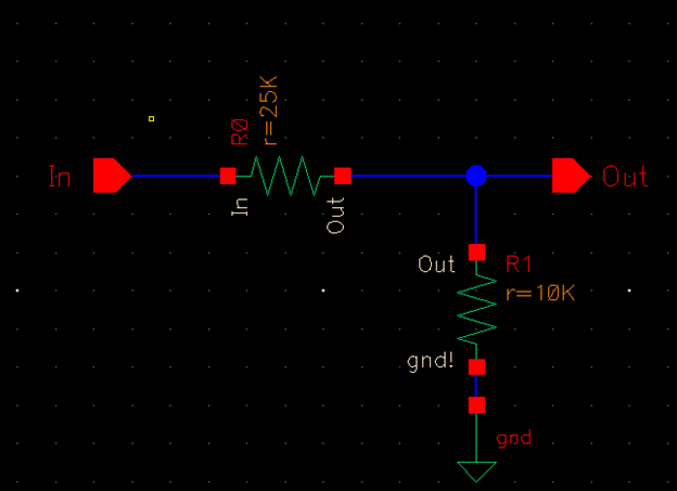
6) A 25K resistor, and use the 25K resistor and a 10K resistor to implement a voltage divider.
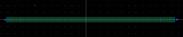
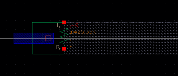
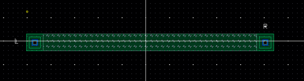
Layout of the 25K resistor:
Layout of the 10K resistor:
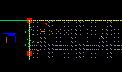
Schematic of the voltage dividier:
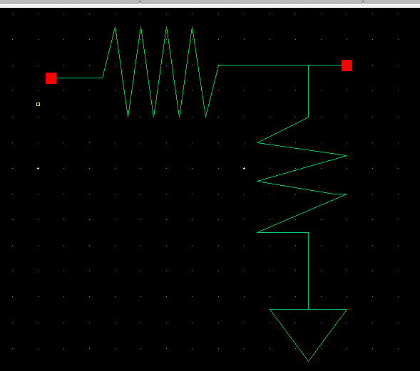
Symbol of the voltage divider:
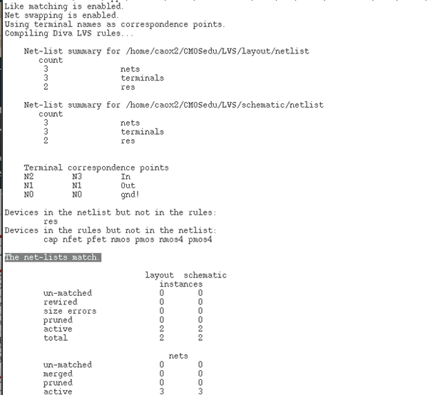
Input: pin<15>
output: pin<16>
VDD: N/A
GND: pin<20>(shared ground)
To test the voltage divier of the chip, just provide the input to the pin<15>, then output will be generated at pin<16>.
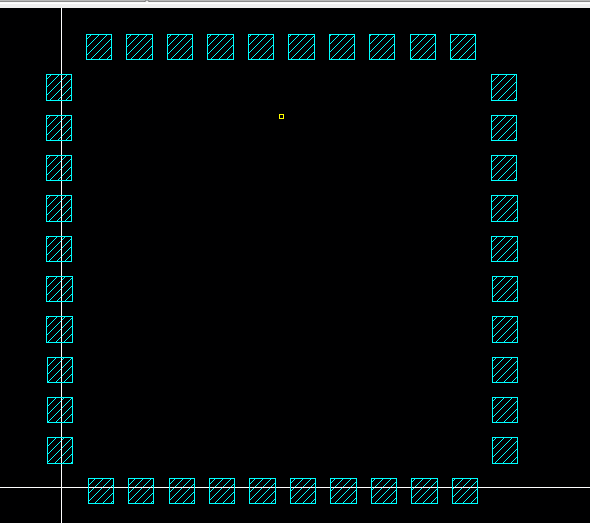
7) Chip Layout:
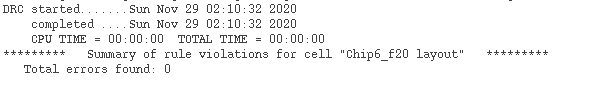
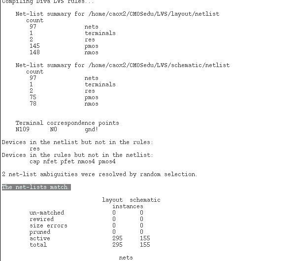
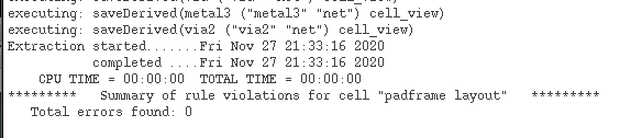
Now the chip is read to submite for fabrication.
for back-ups:
The design director for the test chip can be downloaded here: Chip6_f20.zip
This concludes the Lab 8.