Lab 5 - EE 421L
Authored
by Steve Salazar Rivas
Email: salazs3@unlv.nevada.edu
October 9, 2019
Prelab: For lab 5, we went through Tutorial 3 in order to draw the schematic, layout, and corresponding symbol of a CMOS inverter.
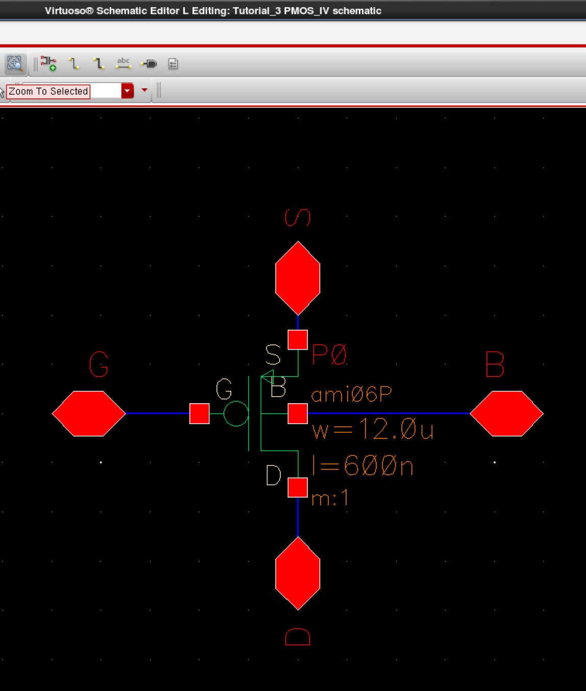
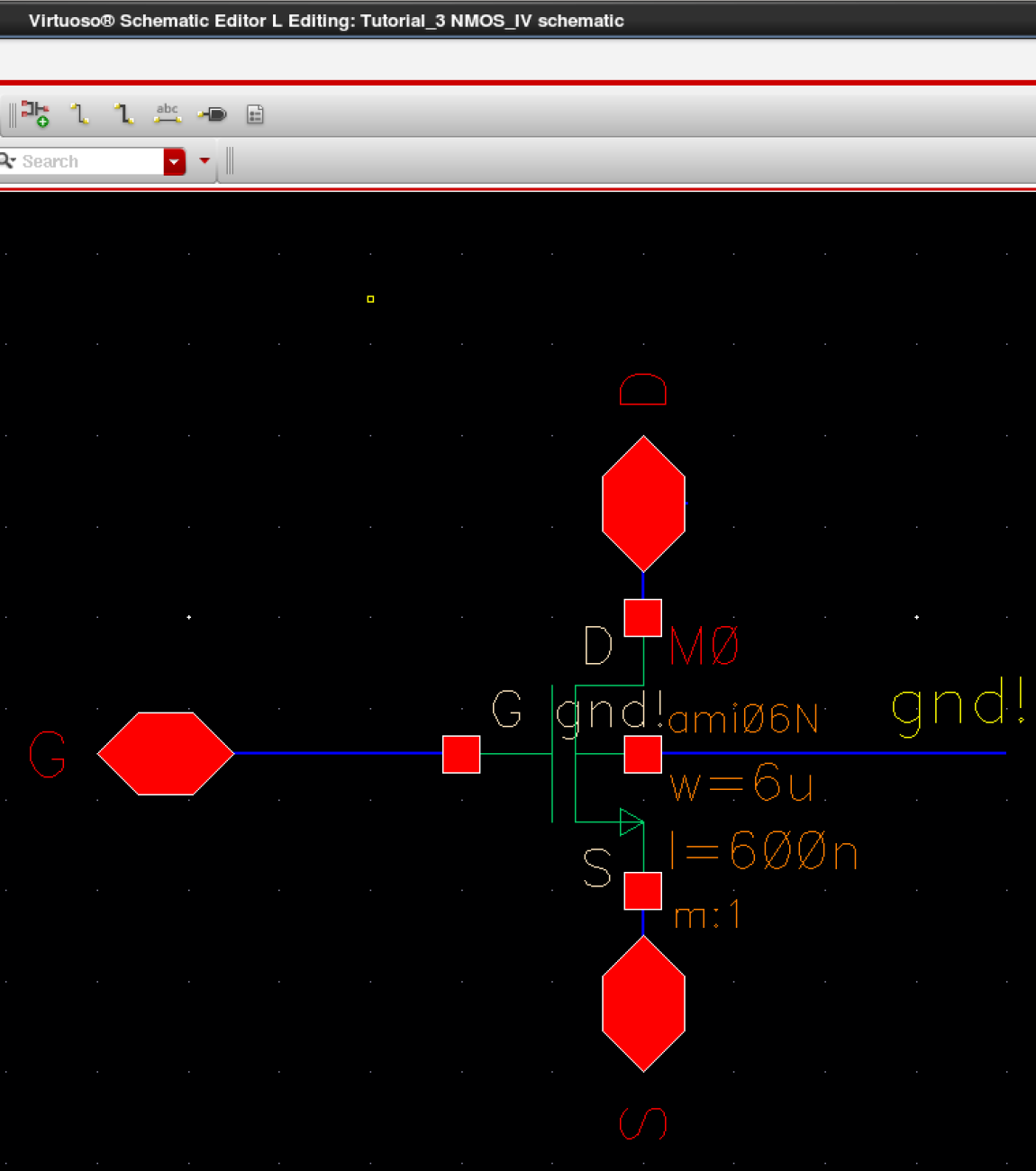
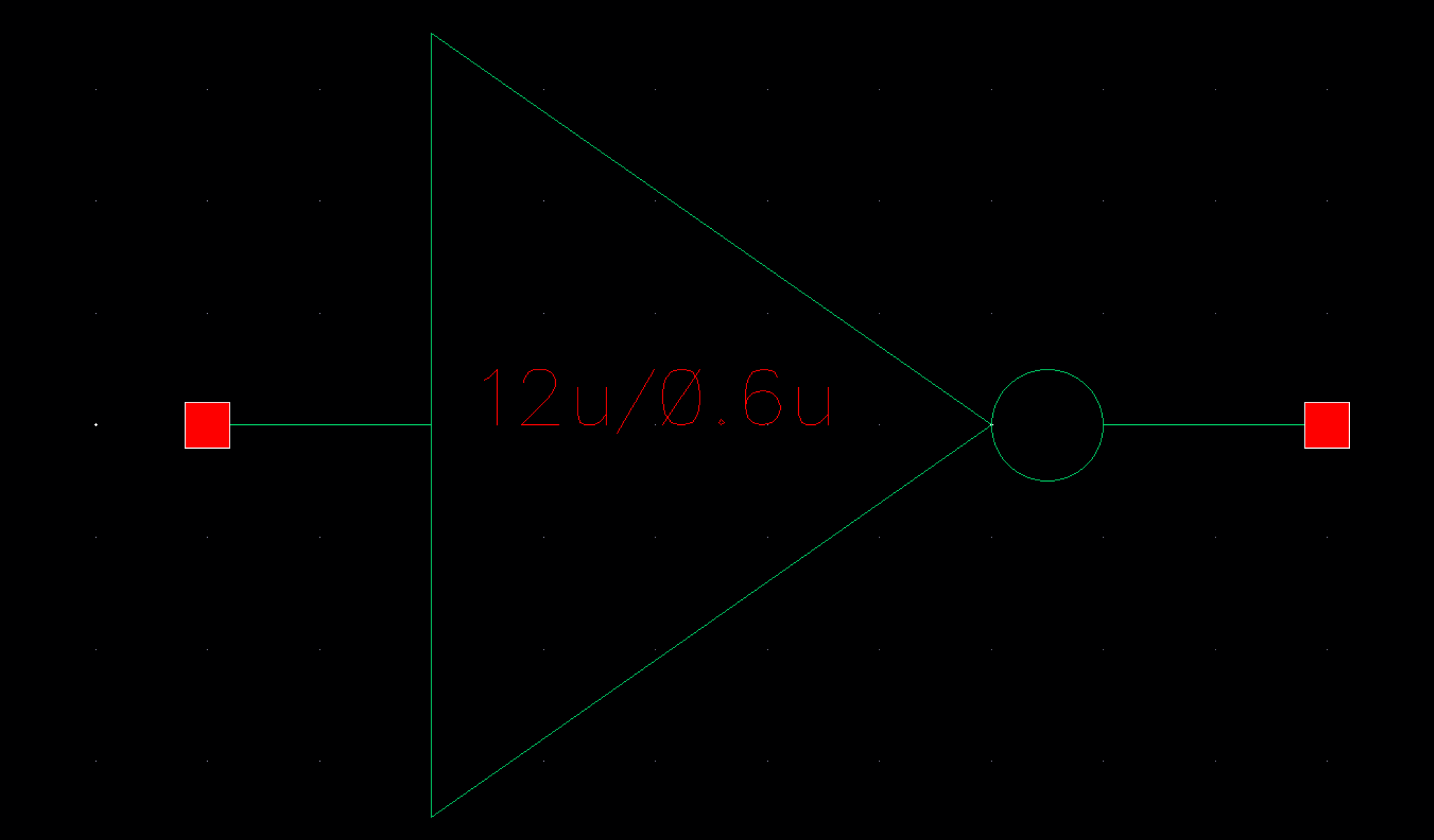
This is our 12u/600n PMOS schematic and NMOS 6u/600n schematic, respectively.
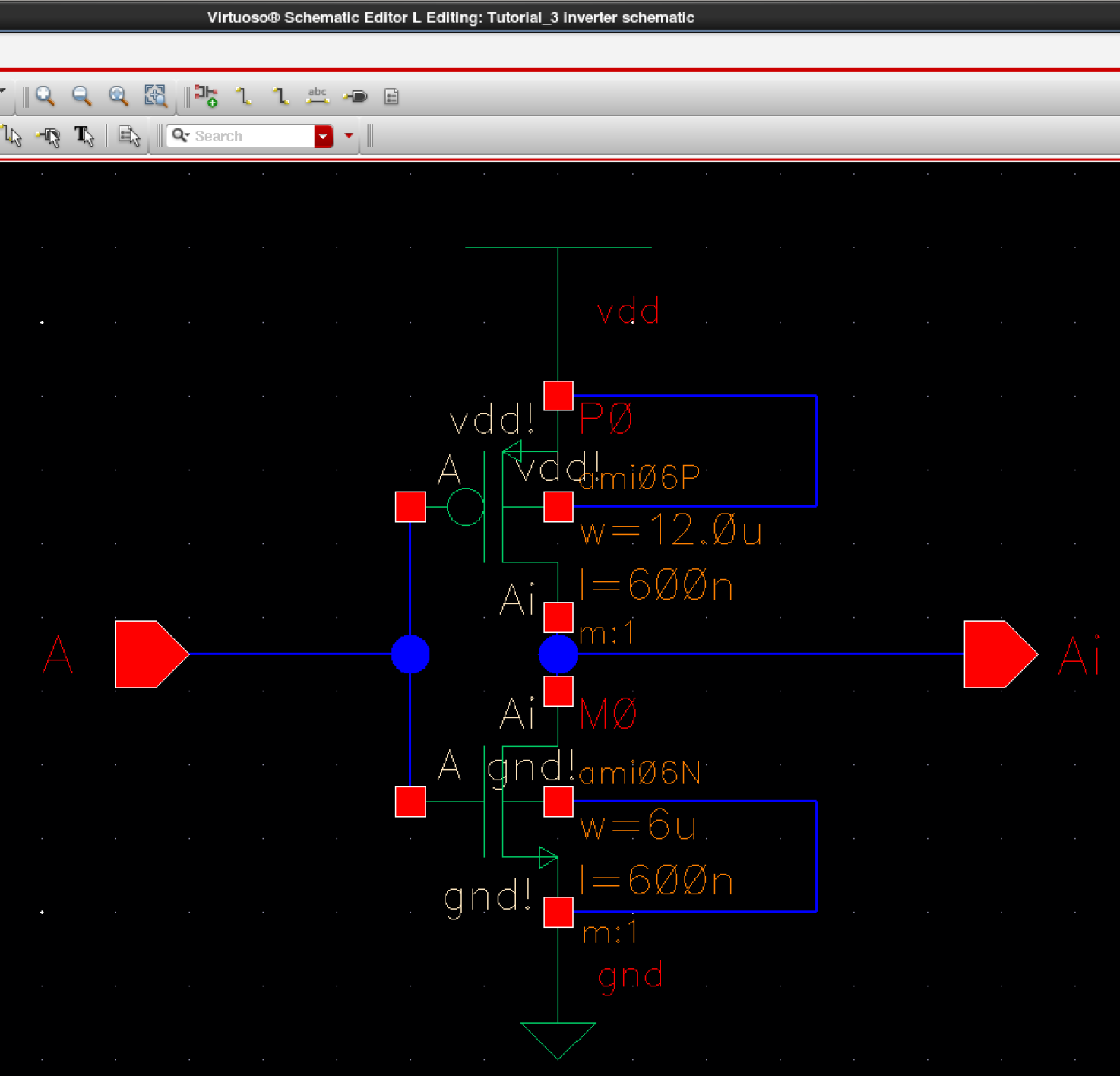
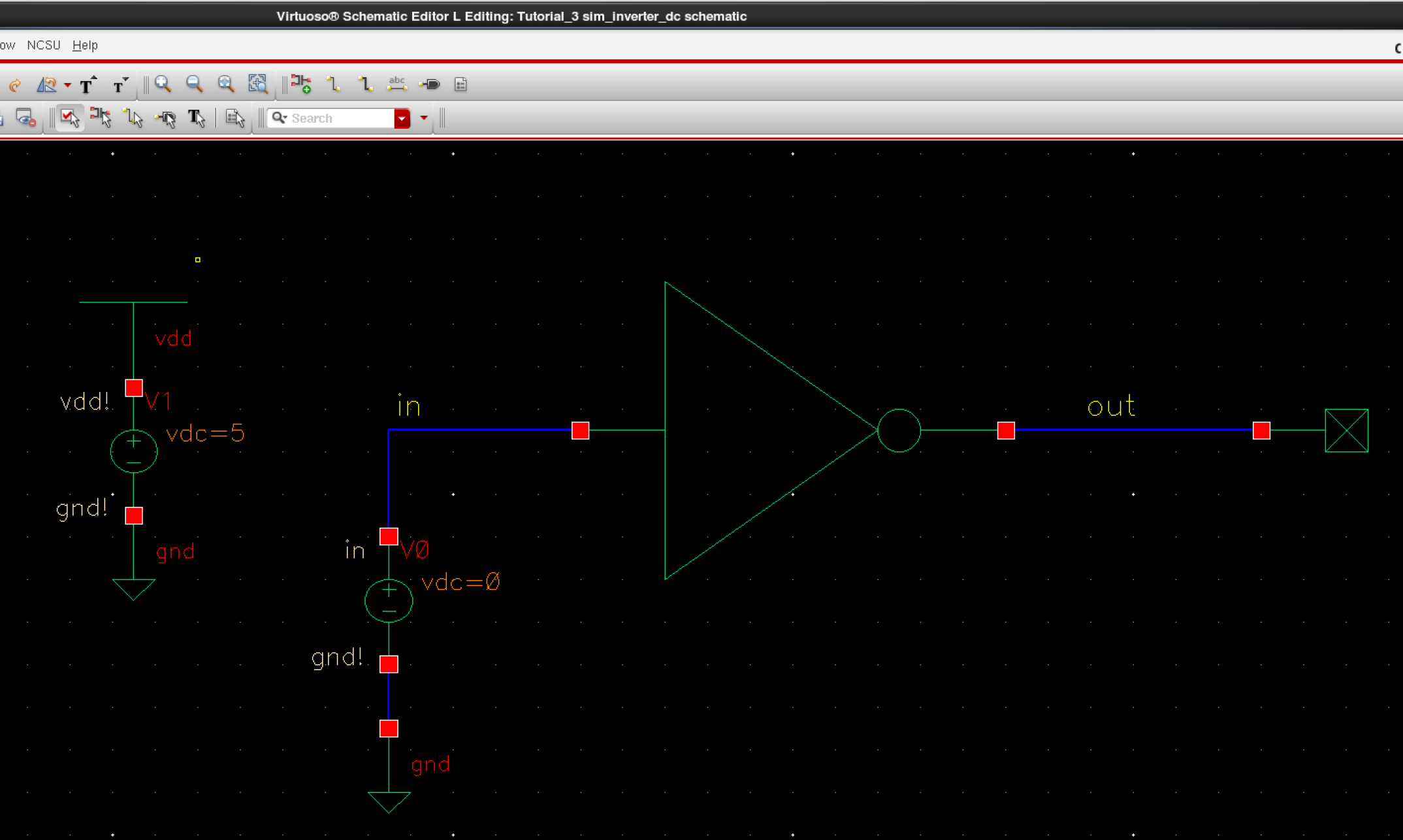
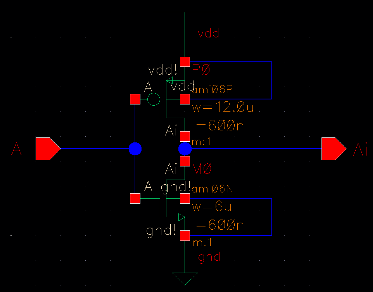
This is our inverter schematic with our PMOS and NMOS connected together and our simulation inverter schematic, respectively.
This is the layout and corresponding extracted view of our inverter
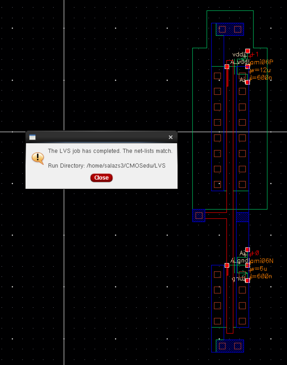
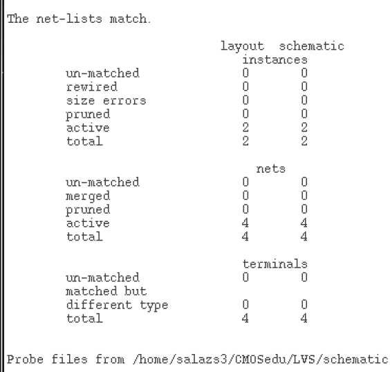
We made sure to LVS our schematic and extracted views, respectively.
Our net-lists match perfectly...
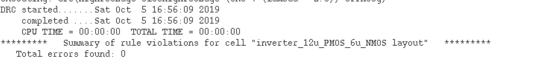
Our layout underwent DRC with minimal effort
Postlab:
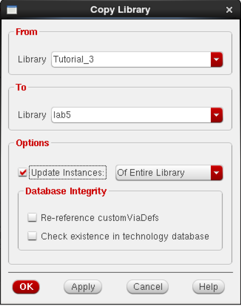
First off, we made sure to copy the Tutorial 3 library into our newly made lab 5 library before starting off.
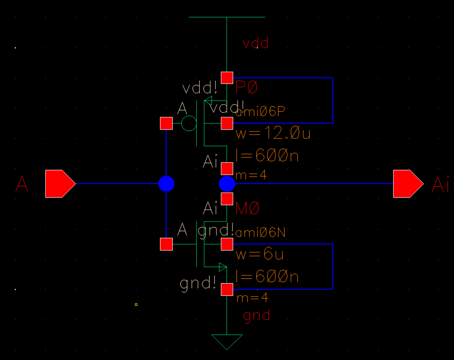
We started off with the 12u/0.6u PMOS and 6u/0.6u NMOS inverter schematic making sure to label the input pin as "A" and the output pin as "Ai"
This is the symbol for our previously mentioned inverter
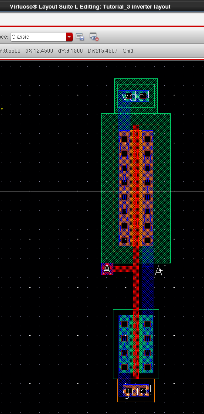
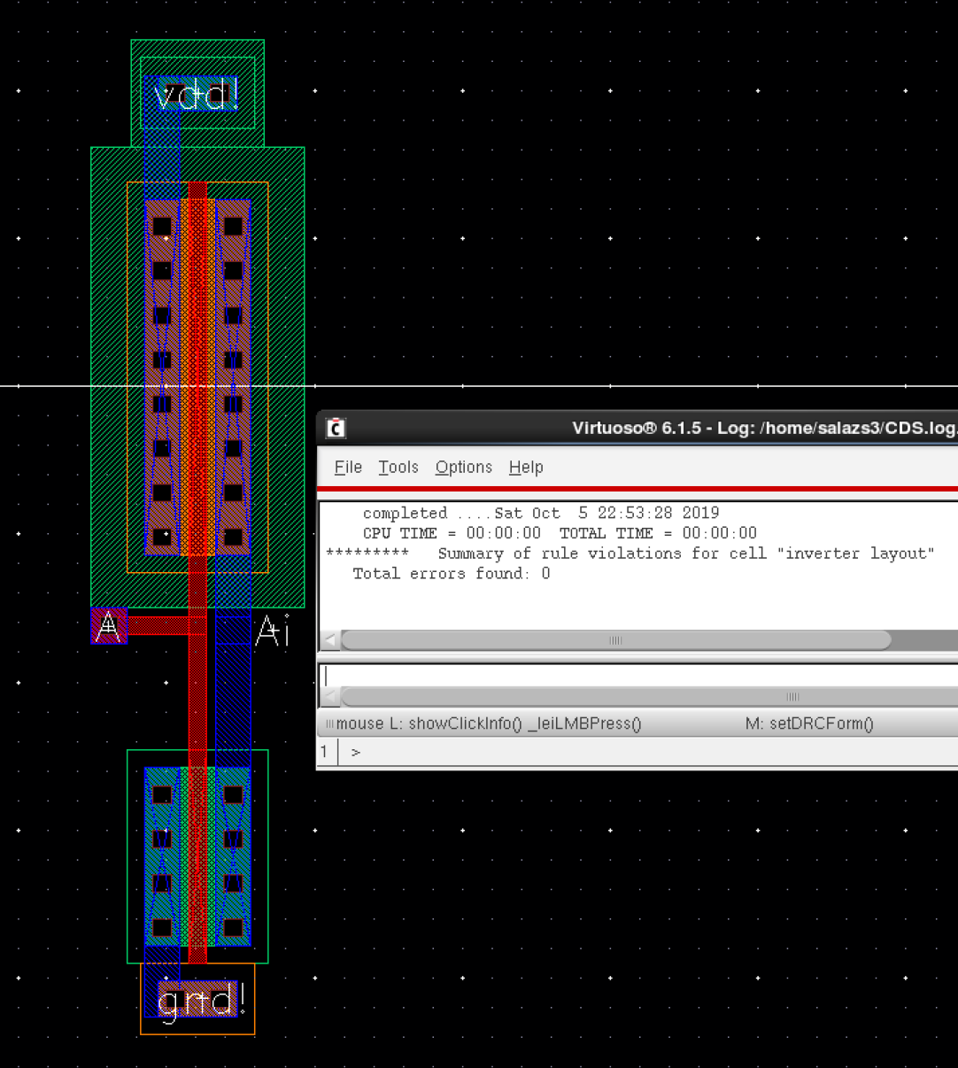
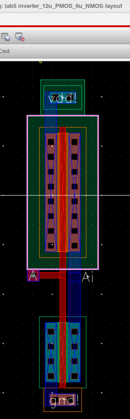
This is the layout view of our inverter
This shows our layout underwent DRC flawlessly...
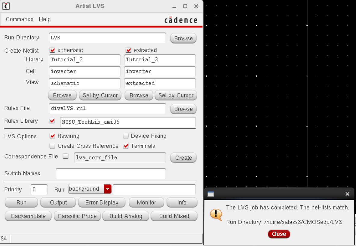
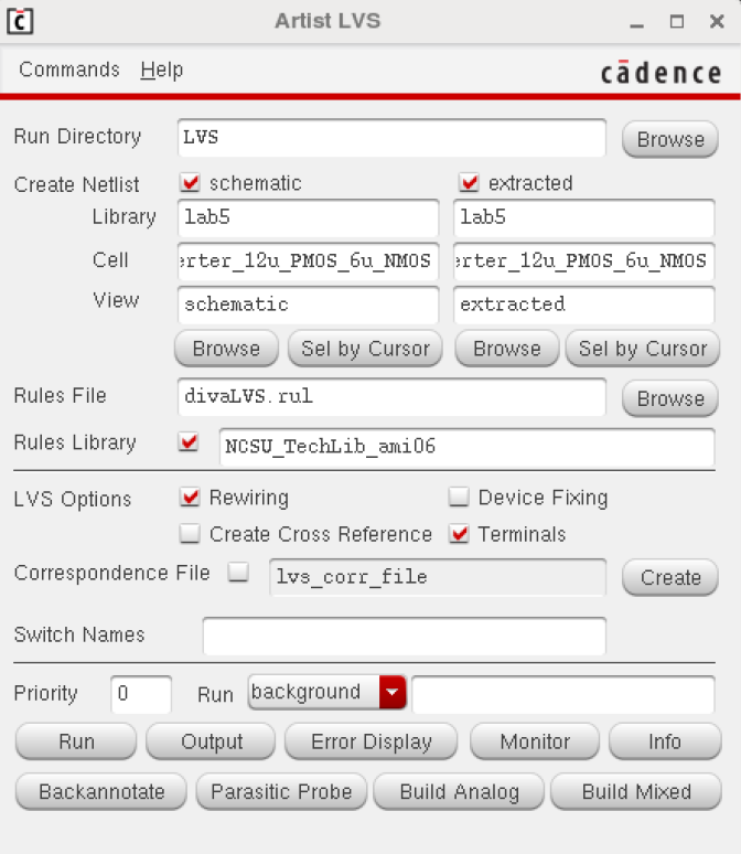
This is our Artist LVS window in order to check our schematic and extracted cell views of our inverter
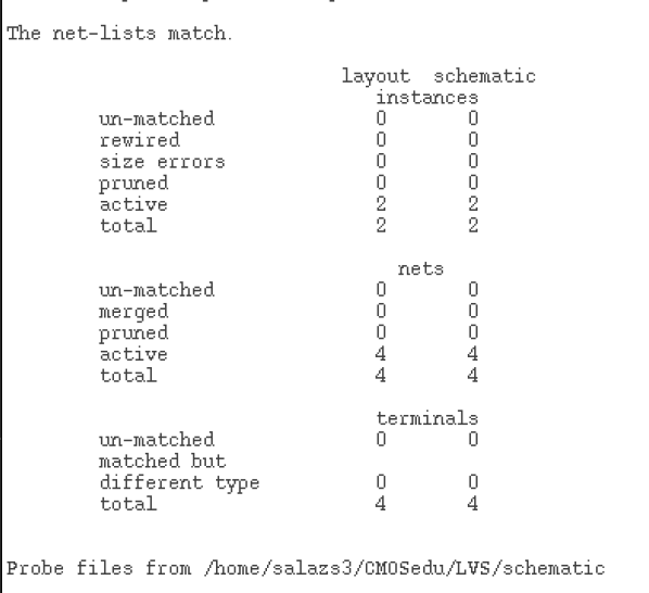
Thankfully, the net-lists matched with minimal effort.
Here is the extracted cell view used in the LVS process.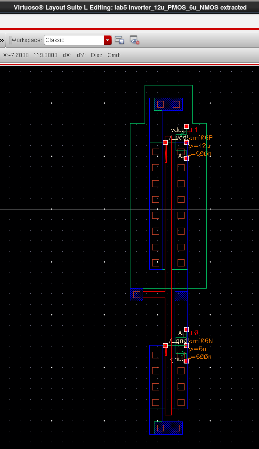
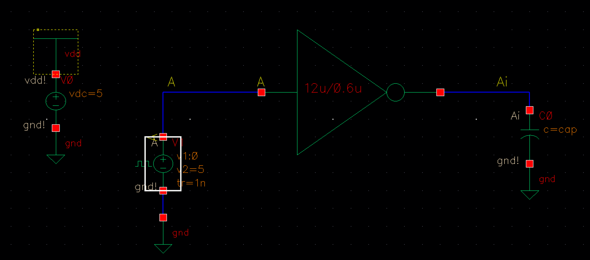
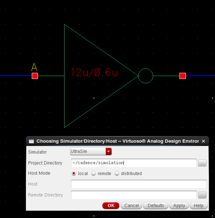
In order to simulate our 12u/6u inverter, we created the schematic below.
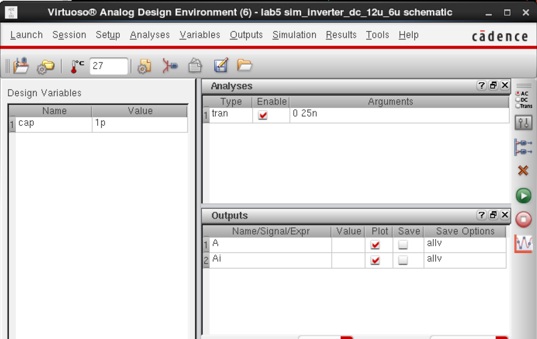
This
window shows us launching the ADE L environment and making sure we
added our proper model libraries, design variables, and a transient
analyses.
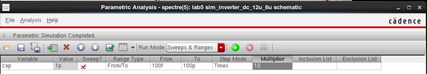
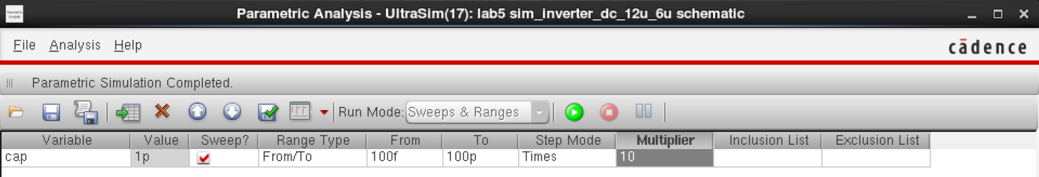
We underwent parametric analysis for our inverter 12u/6u inverter
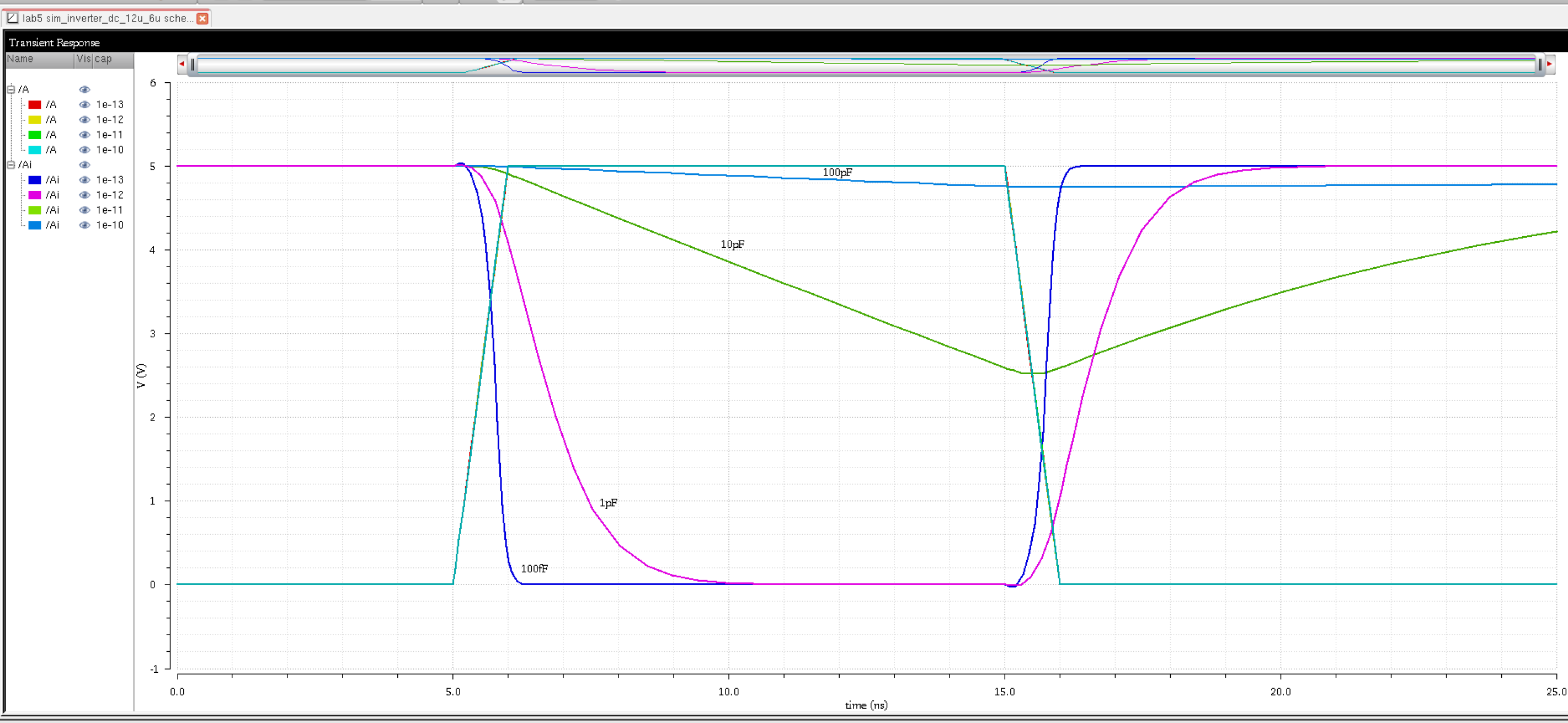
Here
are the simulation results of our 12u/6u inverter with varying
capacitors... As capacitor value increases, the rise and fall times
increase, respectively.
In contrast, we utilized the UltraSim simulator in ADE L using the previous analysis conditions...
We can see in our parametric analysis window that we are truly using UltraSim...
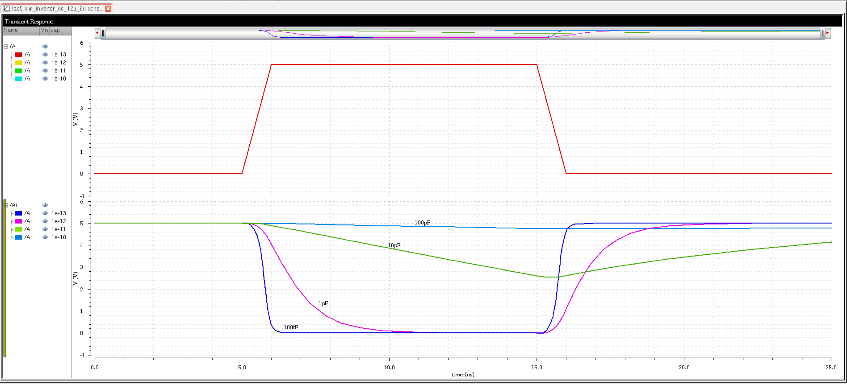
Here are the similar results using UltraSim...
Switching gears to our 48u/0.6u PMOS and 24u/0.6u NMOS flavor using a multiplier of 4...
Here is our schematic view of our 48u/0.6u PMOS and 24u/0.6u NMOS flavor schematic... pay close attention to the m=4
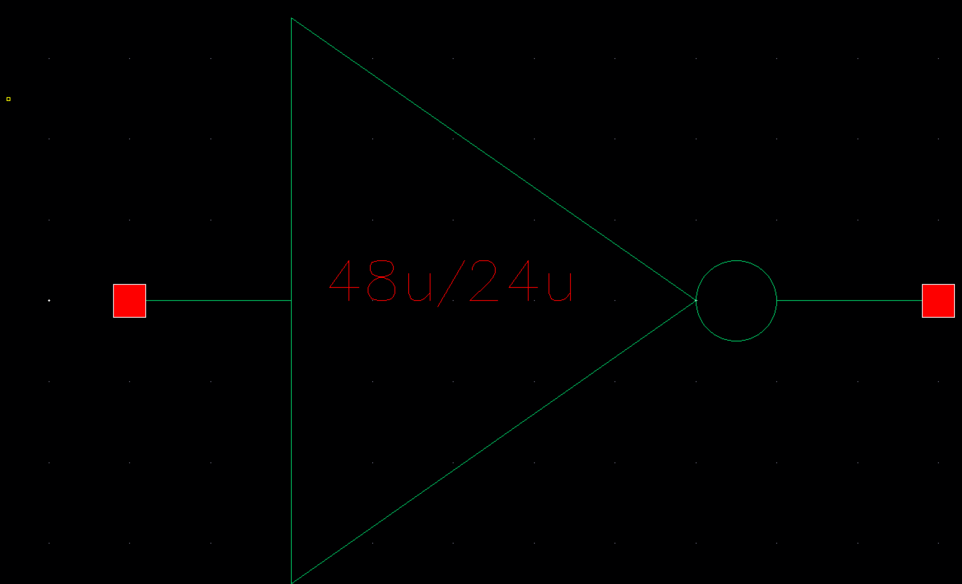
This is the symbol for our 48u/0.6u PMOS and 24u/0.6u NMOS flavor inverter
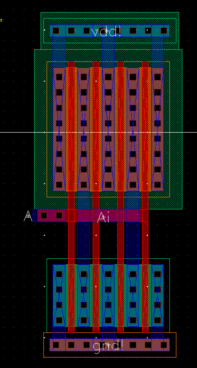
This is the layout view of our 48u/0.6u PMOS and 24u/0.6u NMOS flavor inverter
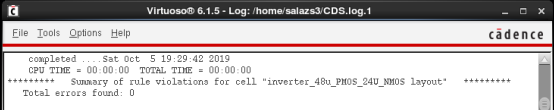
Our layout view underwent DRC beautifully...
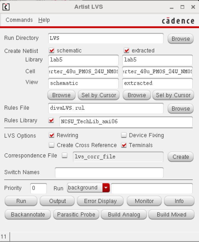
This is our Artist LVS window showing our corresponding schematic and extracted cell views being used
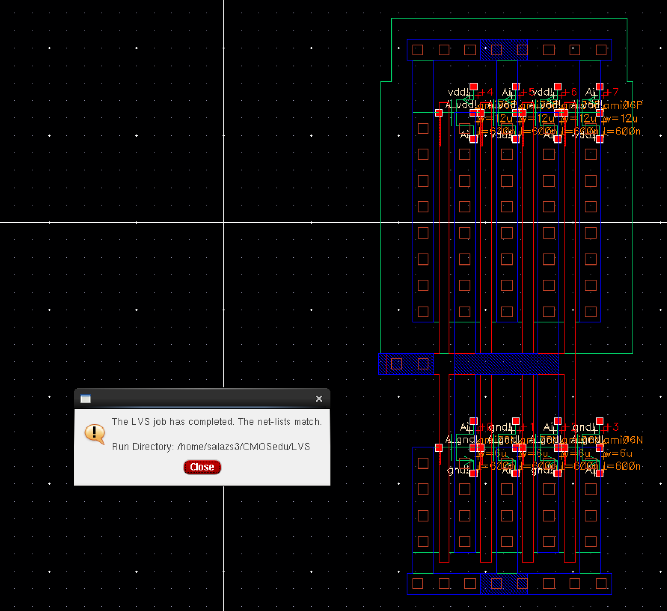
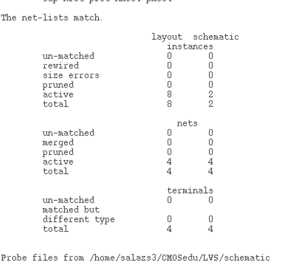
LVS went quite well with the net-lists matching (with the extracted view seen below)...
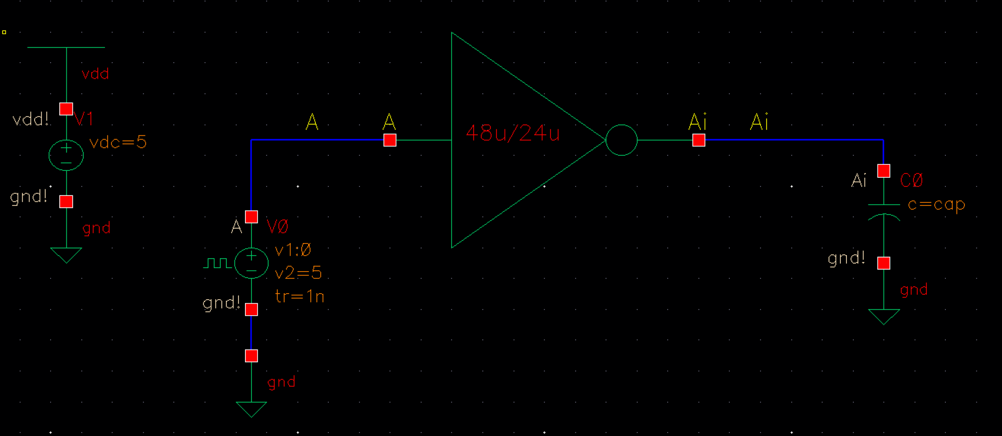
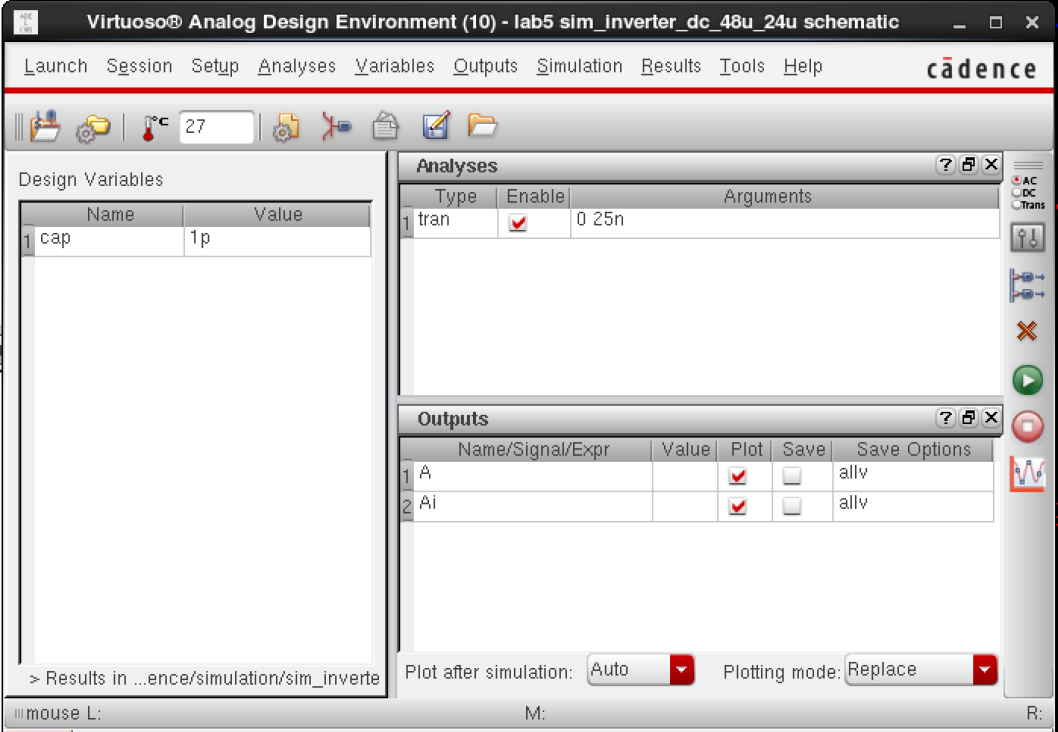
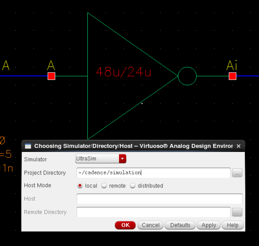
In order to simulate our inverter, we created a simulation schematic as seen below...
This was our ADE L window with the correct design variables, analyses, model libraries, and outputs listed.
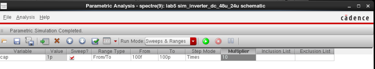
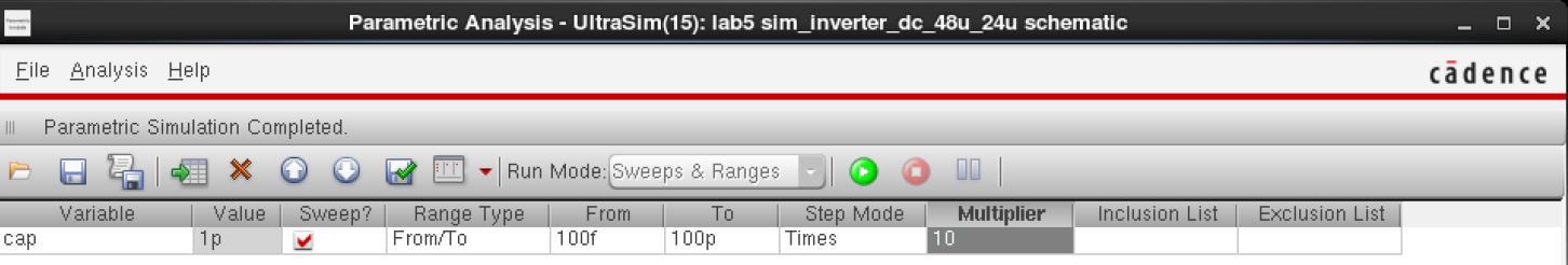
We made sure to correctly undergo parametric analysis...
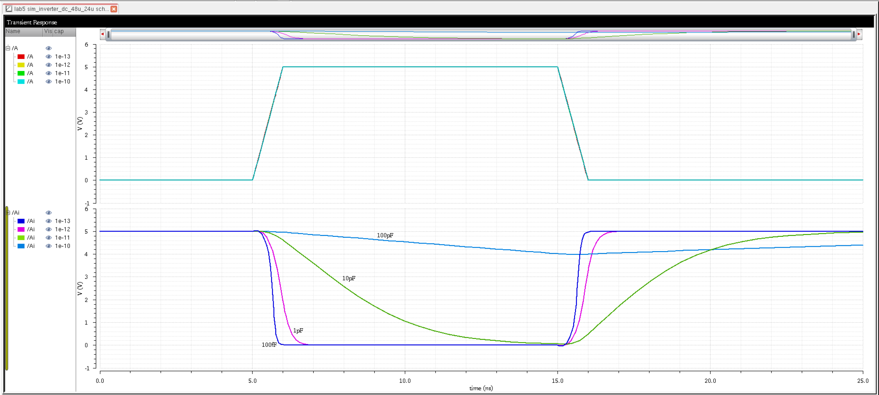
These are the simulation results of our 48u/0.6u PMOS and 24u/0.6u NMOS flavor inverter
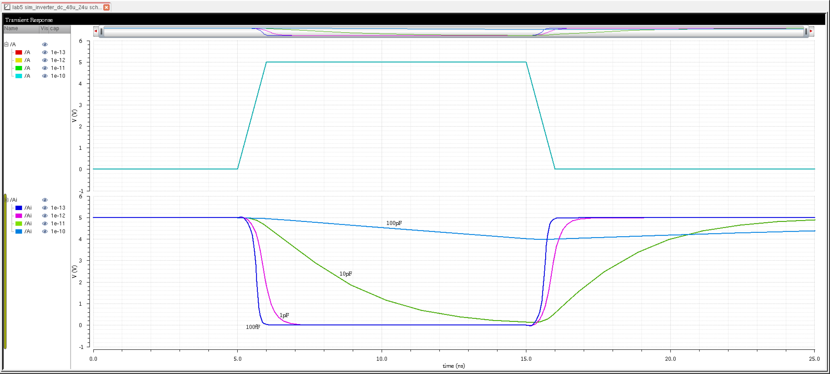
In contrast, we utilized UltraSim to undergo simulations for our 48u/0.6u PMOS and 24u/0.6u NMOS flavor inverter
We can double check and make sure we underwent UltraSim simulation by checking our Parametric Analysis window
Here is our simulation results using UltraSim simulator... pretty similar to using Spectre
Return to salazs3
Return to EE 421L Labs