Lab 3 - ECE 421L
Authored
by Byron Gorsuch,
gorsuch@unlv.nevada.edu,
September 19, 2017
Lab Description
This
lab will continue the development of the 10-bit DAC from lab 2. In this
lab, the layout of the DAC will be created by using n-well resistors
and metal 1 for connections.
Prelab
Tutorial 1 was completed in order to layout a 10K Ohm n-well resistor which will be used to create a layout for the DAC schematic created in lab 2.

Figure
1: 10k n-well resistor layout
In
order to determine the length and width of the n-well to create a 10k
resistor, the considerations of the C5 process from MOSIS were used.
- n-well material is about 800 Ohms/square
- Minimum width of the n-well is 12λ
- λ for the C5 process is 0.3µm
Using
this information the minimum width for the resistor is 3.6 microns. At
800 Ohms a square, in order to achieve a resistance of 10k Ohms it can
be calculted that 12.5 squares are needed.
By choosing the width to
be 4.5 microns as in tutorial 1, it can then be calculated that the
length must be about 4.5 * 12.5 microns or about 56 microns, however in
order for the resistor to fit the
edges on the grid a length of 56.1 microns was used.

Figure 2: 10k
n-well extracted view
Lab
The
n-well resistor created in the prelab was used in order to layout a
10-bit DAC using the R-2R structure. By using the ruler tool, accessed
by pressing 'K' in Virtouso, the exact dimensions of the n-well
resistor could be calculated as well as the minimum distance between n-wells (18λ = 5.4 microns).


Figure
3: DAC Layout
Figure 4: DAC Layout
Close-up
Figure 5: Extracted View of
DAC Layout
Once the layout was complete, the
validity of the layout could be checked using the Design Rule
Checking(DRC) tool. If the DRC is successful, the command interpreter
window will display the tests run and report zero errors found.

With a DRC the extracted view of the layout can be created. A close-up
of the ectracted view of the layout can be seen in Figure 5 above.
The extracted view will display the value of each n-well resistor as
well as any pins connected to the node being observed.
To ensure that the DAC layout is in fact the correct layout of the
schematic from lab 2, the extracted view can be compared to the
schematic
for verification using the Layout-Versus-Schematic (LVS) tool.
With matching netlists, the extracted view can faithfully be used in
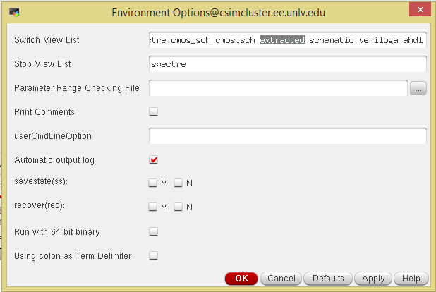
order to simulate the layout. This can be done by opening the Spectre
simulation tool and selecting Setup -> Environment. From this
window, simply enter the word "extracted" before the word "schematic"
as shown
in figure 8 below. Once this is done the simulation can be performed as usual.
Figure 6: DRC Success


Figure 7: LVS Success
Figure 8: How to Sim Extracted View


Figure
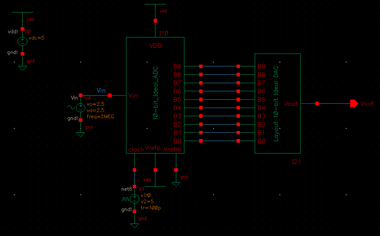
9: Test Schematic
Figure 10:
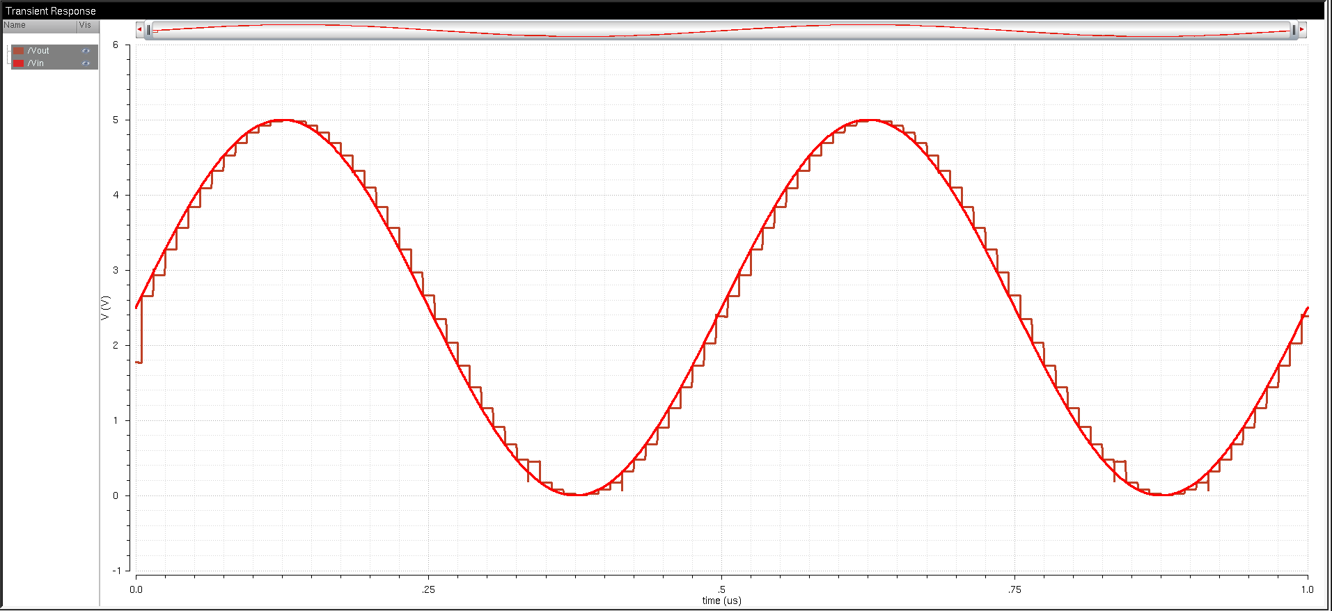
Simulation Results
The schematic used to test
the DAC created with the layout is the same as in lab 2. As can be seen
in figure 10 above, the behavior of the DAC is as expected based on the
simulations from lab 2.
The files used for this lab can be found here
Return to my lab directory
Return to CMOSedu.com