Lab 2 - ECE 421L
Authored
by Byron Gorsuch,
gorsuch@unlv.nevada.edu
September 12, 2017
Lab
description:
This lab demonstrates the design and function of a 10-bit Digital-to-analog converter (DAC).
Prelab:
The files for the lab were downloaded from CMOSedu.com here. Afterwards they were uploaded, unzipped, and added to my library directory on Xterm.
The sim_Ideal_ADC_DAC schematic was opened and simulated, obtaining the following results:

Figure 1: Schematic of DAC
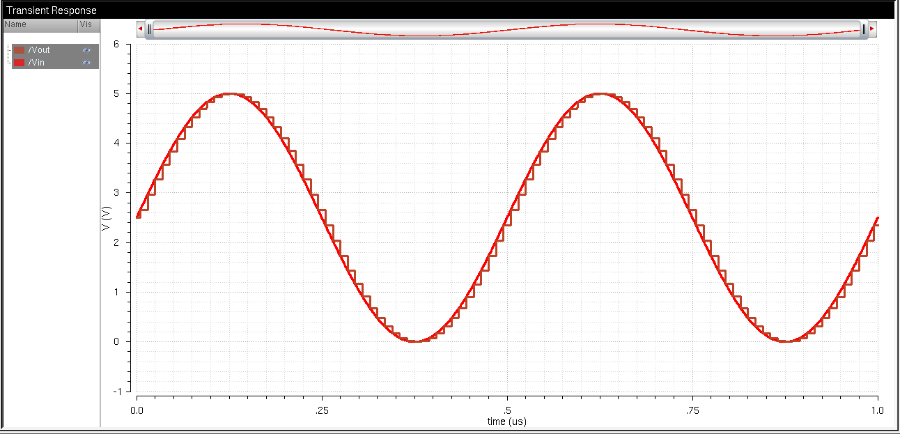
Figure 2: Output of
DAC 5 Volts
As can be seen, the output is a discrete function of the input where each bit change from B[9:0] represents
an incremental change in the input voltage. The increment can be
calculated by dividing the magnitude of the input by the maximum value
possible with the number of bits (2n, where n is the number of bits).
To demonstrate, the magnitude and reference voltage were changed to 8 Volts for the following result:

Figure 3: Output of DAC 8 Volts
Lab:
To begin, a 10-bit DAC schematic was created using n-well resistors valued at 10k as follows:

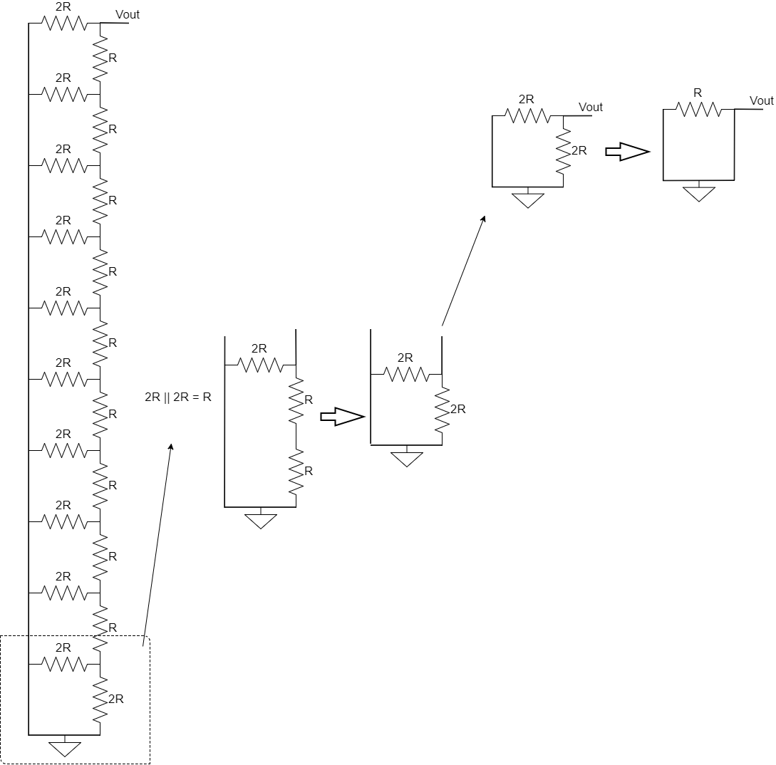
The resistance of the DAC can be calculated by combining the resistors in series and in parallel.

Figure 4: R-2R
DAC
Figure 5: Calculating Output
Resistance
The equivalent resistance of the circuit was found to be simply R, or in this case 10k Ohms.
Next,
the circuit was used to drive a 10 pF load by grounding all of the
inputs except B9 which was connected to a pulse source (0 to 5 V),
As
calculated above, the equivalent resistance of the circuit is 10k Ohms.
Therefore, the delay should be calculated using 0.7RC.
0.7(10k)(10p)=70 ns
In
order to simulate and verify this result, the schematic from Figure 4
above was turned into a symbol by copying the existing ideal DAC
symbol, removing
the unneeded pins and replacing its schematic with the R-2R schematic.
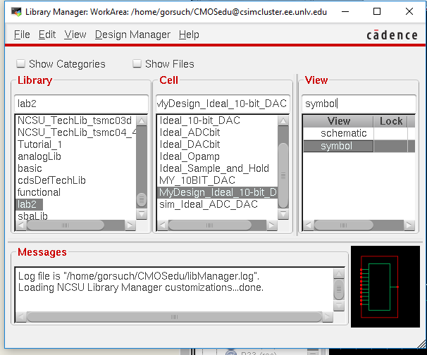


Figure 6: Copying Cell
Figure 7: Original Symbol
Figure 8: My Symbol
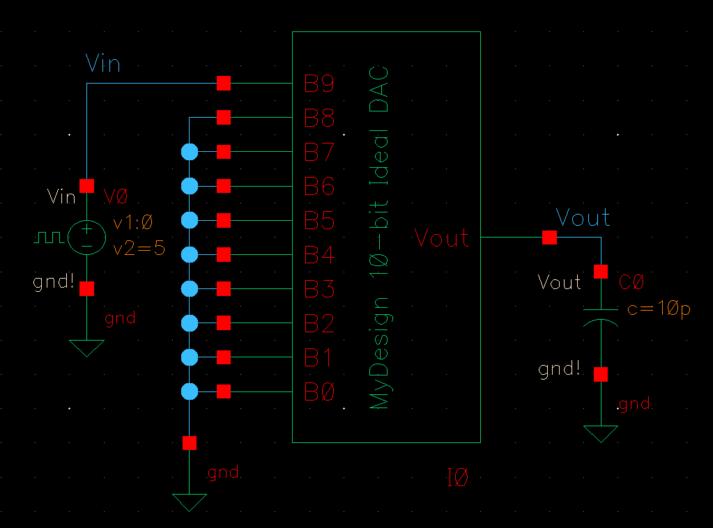
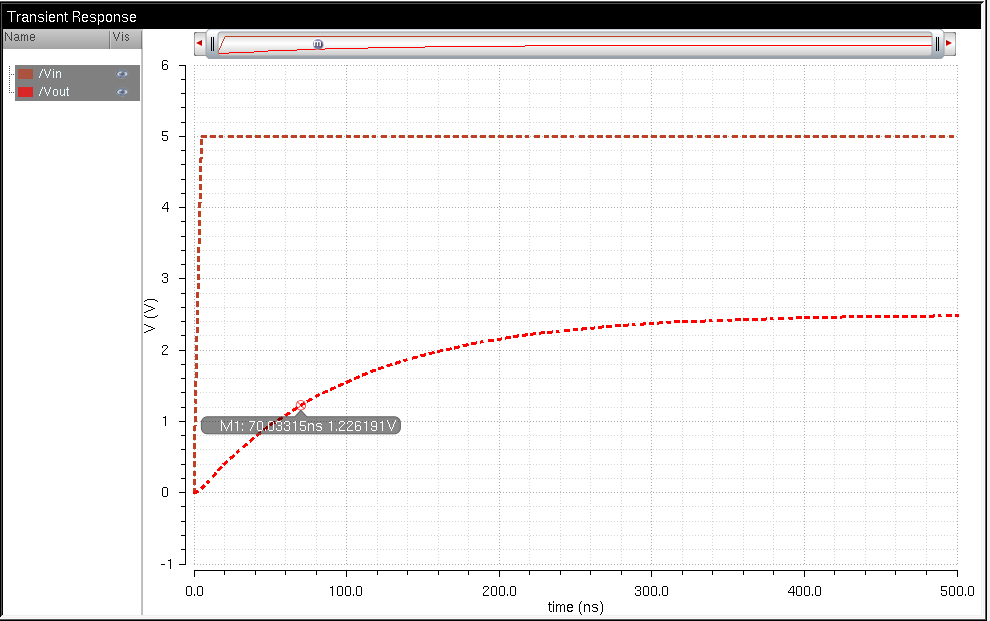
Figure 9: Driving a 10pF load
Figure 10: Simulation Results for Driving 10pF load
As can be seen in figure 10 above, the delay when driving the 10 pF load is as calculated 70 ns
Next,
the newly created symbol of the 2R-R schematic was used to replace the
ideal DAC which was tested above in the prelab to verify
how the 2R-R DAC compares.

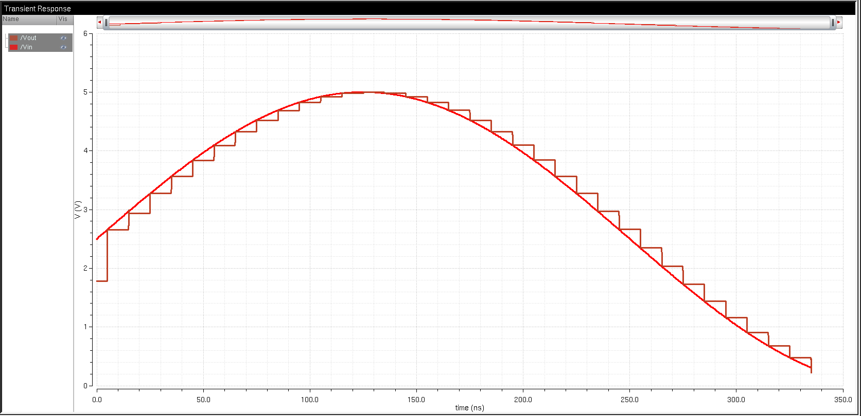
Figure 11:
Replacing Symbol
Figure 12: 2R-R DAC
Performance
As can be seen by the waveform, the 2R-R DAC performs extrememly well when compared to the ideal DAC waveform.
The design was further tested by observing the effects of adding a load to the output. The following results were found:
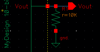
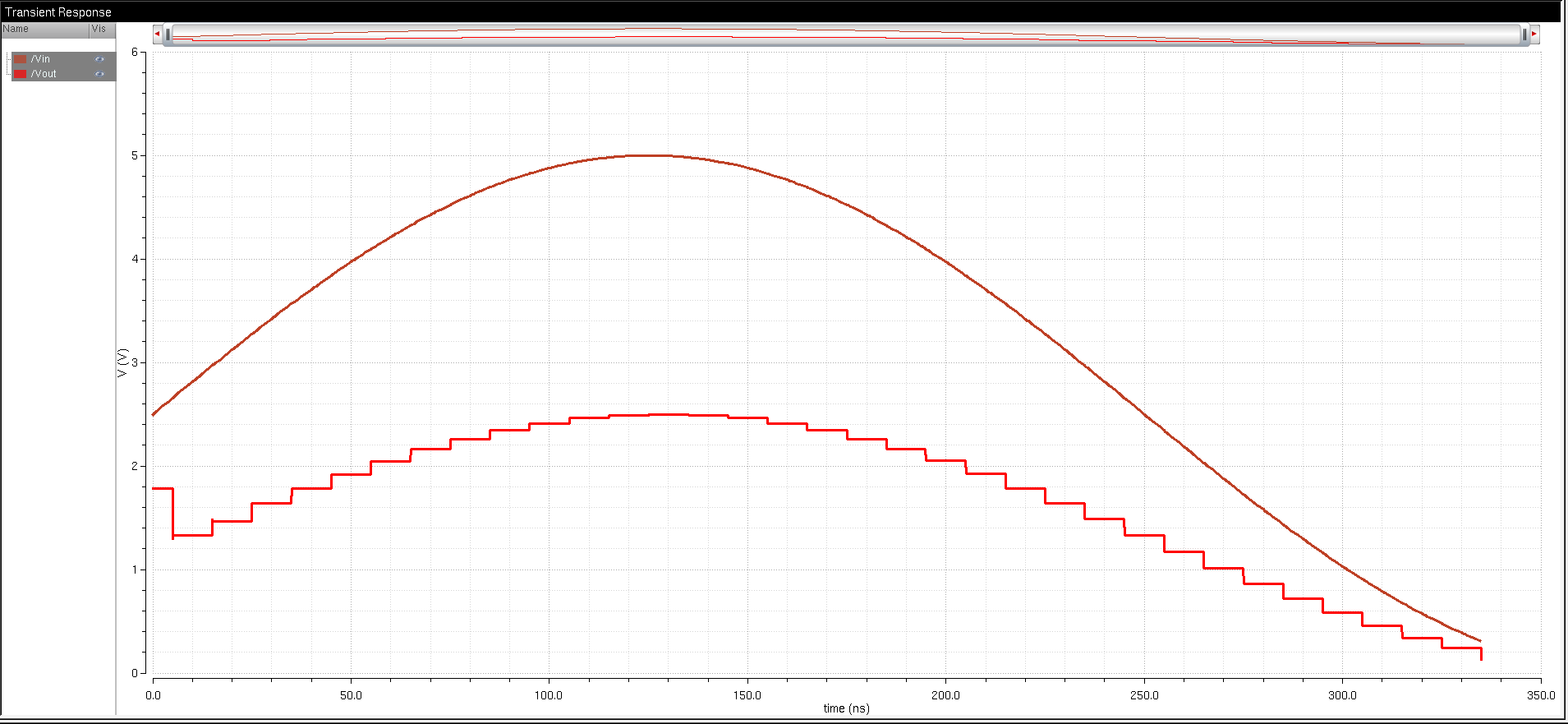
Figure 13: Resistive
Load
Figure 14: Simulation Results for
Driving Resistive load 10k
By adding a 10k
Ohm load, the output voltage dropped to half of the original value.
This is because the DAC resistance is 10k so by adding a 10k resistor
in parallel, the output divided by half.
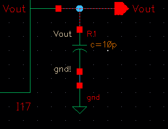
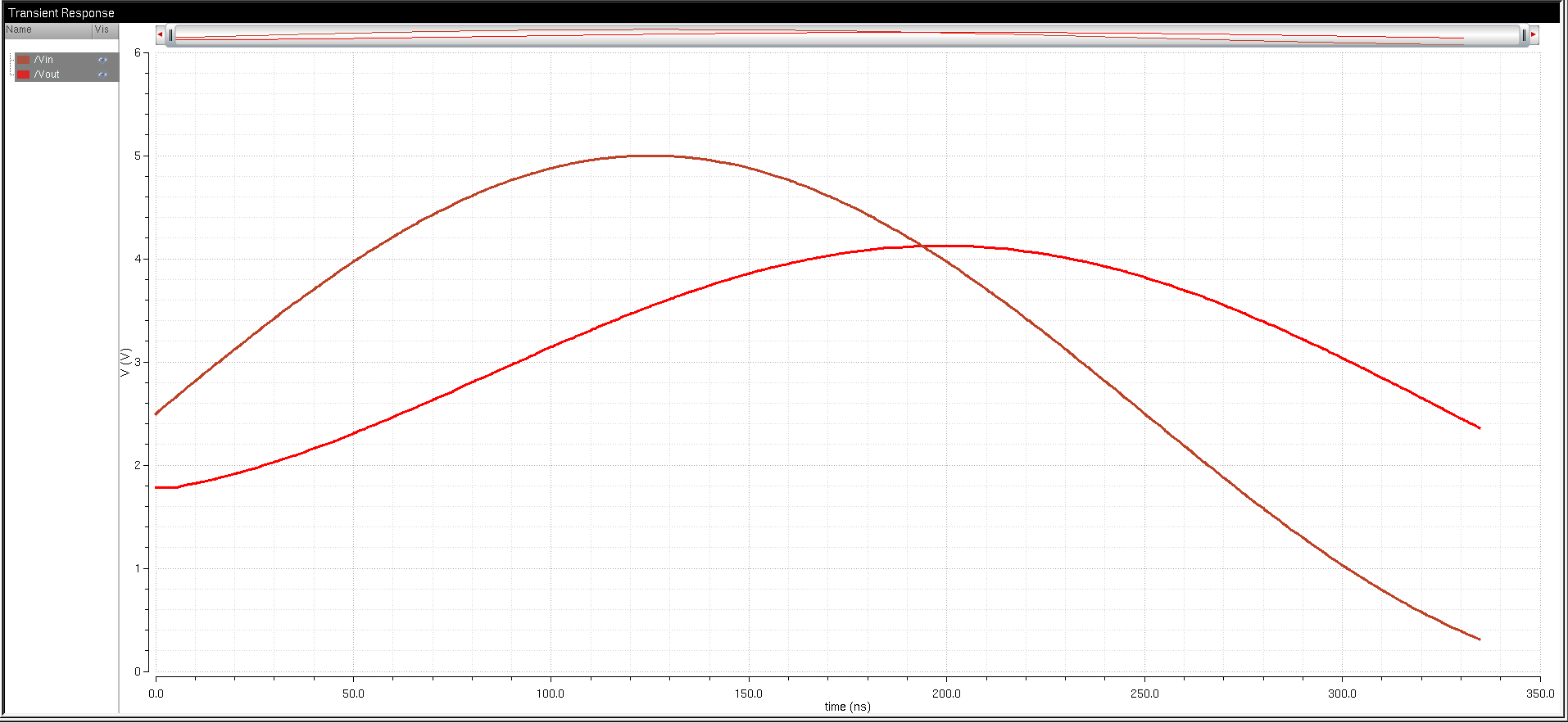
Figure 15: Capacitive
Load
Figure 16:
Simulation Results for Driving Cap load 10p
The
capacitive load causes an RC time delay which in turn smooths the ouput
signal out, but also puts the input and output signals out of phase.

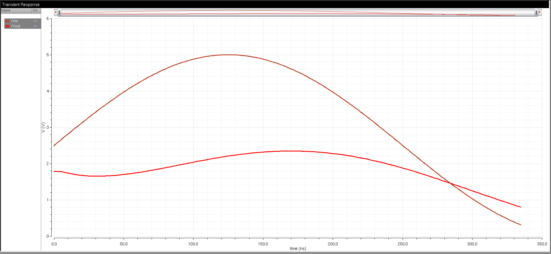
Figure 17: RC
load
Figure 18:
Simulation Results for Driving RC load
The RC
load combines the effects of the resistive and capacitive loads. That
is, the output signal becomes smoothed and out of phase from the
capacitor, and the resistive load causes a change in amplitude.
The
amplitude is based on the resistance. when the output resisitance is
much larger than the resistance from the DAC, the output voltage
shrinks significantly as the effect of the voltage divider increases.
Return to my lab directory
