Lab 4 -
EE 421L
Authored
by Reiner Dizon,
Email: dizonr1@unlv.nevada.edu
Today's
date is September 22, 2017
Lab
description:
This
lab focuses on the construction of NMOS and PMOS layouts and symbols as
well as testing and simulating for their IV characteristics.
PRELAB
- Back-up all of your work from the lab and the course
Lab Backup:

| Course Backup:

|
LAB
REPORT
1) NMOS and PMOS schematics/simulations
For
this first part, I generated four schematic and simulations to show the
IV characteristics of NMOS and PMOS transistors. Each of these set of
schematics and simulations share similar steps of creation, so I
highlighted mostly the difference among them. One major difference is
how to connect the body in both transistors: gnd! for NMOS and vdd! for
PMOS. Not only did I included schematics, I also included the
corresponding symbols used for each one which were based from ones in
the tutorial.
Part A: NMOS device, ID vs VDS
Schematic for 6u/600n (W/L ratio) NMOS device:
 | MOSFET Symbol Used for the schematic:

The NMOS device used for this part came from this symbol.
Notice that the body is connected to ground (gnd!). |
Simulation
for ID vs VDS characteristic curves for VGS varying from 0 to 5V in 1V
steps while VDS varies from 0 to 5V in 1mV steps:

As seen above, there are six graphs in this singular waveform since the variation in VGS is parameterized using Parametric Analysis:

Part B: NMOS device, ID vs VGS
Schematic (similar to Part A, but VDS = 100mV):
 | Simulation:

For this simulation, VGS varies from 0V to 2V in 1mV steps while VDS stayed at 100mV. |
Part C: PMOS device, ID vs VSD
Schematic for 12u/600n (W/L ratio) PMOS device:

Notice that the body (B) is connected to power (vdd!).
| MOSFET Symbol Used for the schematic:

This PMOS device used came from this symbol. |
Simulation for ID vs VSD
characteristic curves for VSG varying from 0 to 5V in 1V steps while
VSD varies from 0 to 5V in 1mV steps:

This simulation also utilizes the Parametric Analysis tool.
Part D: PMOS device, ID vs VSG
Schematic (similar to Part C, but VSD = 100mV):

| Simulation:

For this simulation, VSG varies from 0V to 2V in 1mV steps while VSD stayed at 100mV. |
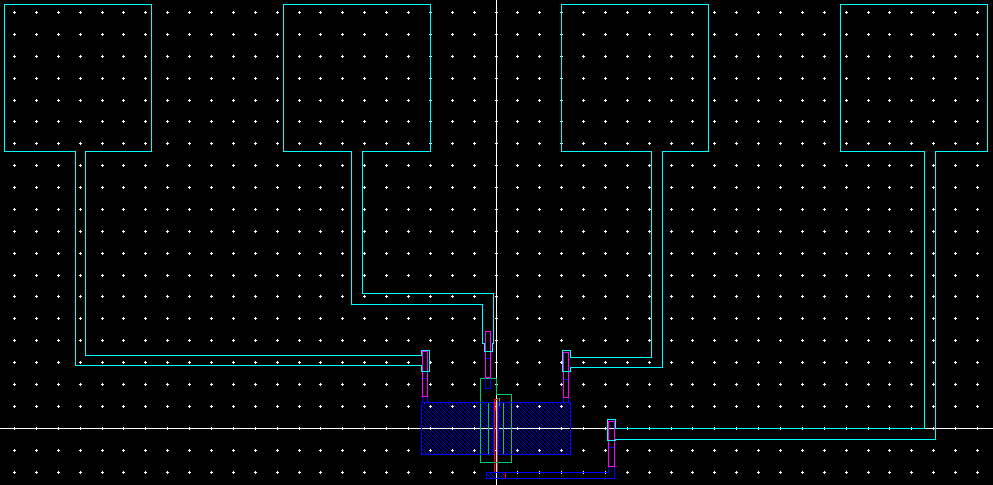
2) NMOS Layout (6u/600n W/L ratio with probe pads)
The
layout used for this part was also based from the tutorial but with the
addition of probe pads which came from lab4 zip file. Since the probe
pad contains metal3 and the MOSFET has metal1 and poly connections,
vias were necessary for connecting metal3 to metal2 (via2) and metal2
to metal1 (via). Three rows of contact are used for each
interconnections to reduce resistance between connections. The probe
pad themselves are spaced 30 microns from each other as specified by
the rule design. After creating the layout, I performed DRC to check
for errors.
After
passing the DRC, I extracted the layout to check if I input the correct
MOSFET parameters as specified from the lab instruction.
Extracted:

| Zoomed In:

|
Before
performing LVS, I made a copy of the corresponding schematic for this
device from part 1 and added the probe pads to match the layout design.
Afterwards, I performed the LVS to check if netlist match.
Schematic:

| LVS Results:

|
3) PMOS Layout (12u/600n W/L ratio with probe pads)
Similarly,
the following layout was an extension of the PMOS transistor created
from the tutorial with probe pads. One key difference between this and
NMOS layout is the presence of the n-well in this design. As done
before with the other layout, the DRC is ran to check for errors. The
layout is then extracted to check if the design matches the
specifications given in the instructions.
Extracted:

| Zoomed In:

|
Finally,
the corresponding schematic for this design from part 1 is copied and
modified with the addition of probe pads. Then, LVS is ran to check if
the netlists match between the layout and schematic.
Schematic:

| LVS Results:

|
After finishing the lab, I backed up my lab 4 web directory from CMOSedu and library from the cluster:
Return
to Reiner's Labs
Return
to EE 421L Labs