Lab 6 - ECE 421L
Authored
by Staford Snow, snows4@unlv.nevada.edu
10/26/2016
Lab
description: In this lab, I drafted schematics, created
symbols, designed layouts, and simulated a 2-input NAND and
XOR gate using 6u/0.6u MOSFETs. Following the completion of the
gates, I drafted a schematic, created a symbol, designed a layout, and
simulated a full adder circuit using my gates.
Pre Lab: Following the lab instruction, I backed up all my work from the lab and the course. I next went through the instruction in Tutorial 4.
Lab:
To begin the lab, I drafted the schematics for the 2-input NAND and XOR gates using 6u/0.6u MOSFETS.


After creating the schematics, I designed the symbols for both gates.


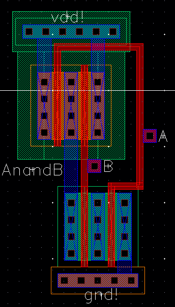
Continuing with the lab, I created the layout for the NAND and XOR gates.


I made sure both layouts passed LVS and DRC.


I next drafted a schematic to simulate my gates. I included an inverter to increase my knowledge.

I
ran the simulation and was able to see that the timing of the input
pulses caused glitches. These glitches are cause, in part, by
propagation delay through the gates.

After completing the NAND and XOR gate, I drafted the schematic for a full adder using the new gates.

After completing the schematic, I created a symbol for this cell.

Once I had the symbol completed, I used it in a schematic to run simulations.

I ran the simulation and was able to see the schematic working.

I next designed a layout for the full adder using the gates I made earlier.

The layout passed DRC and LVS.


I have included my zipped library here.
This concluded the requirements of lab 6.
Return to my labs
Return to EE421L

