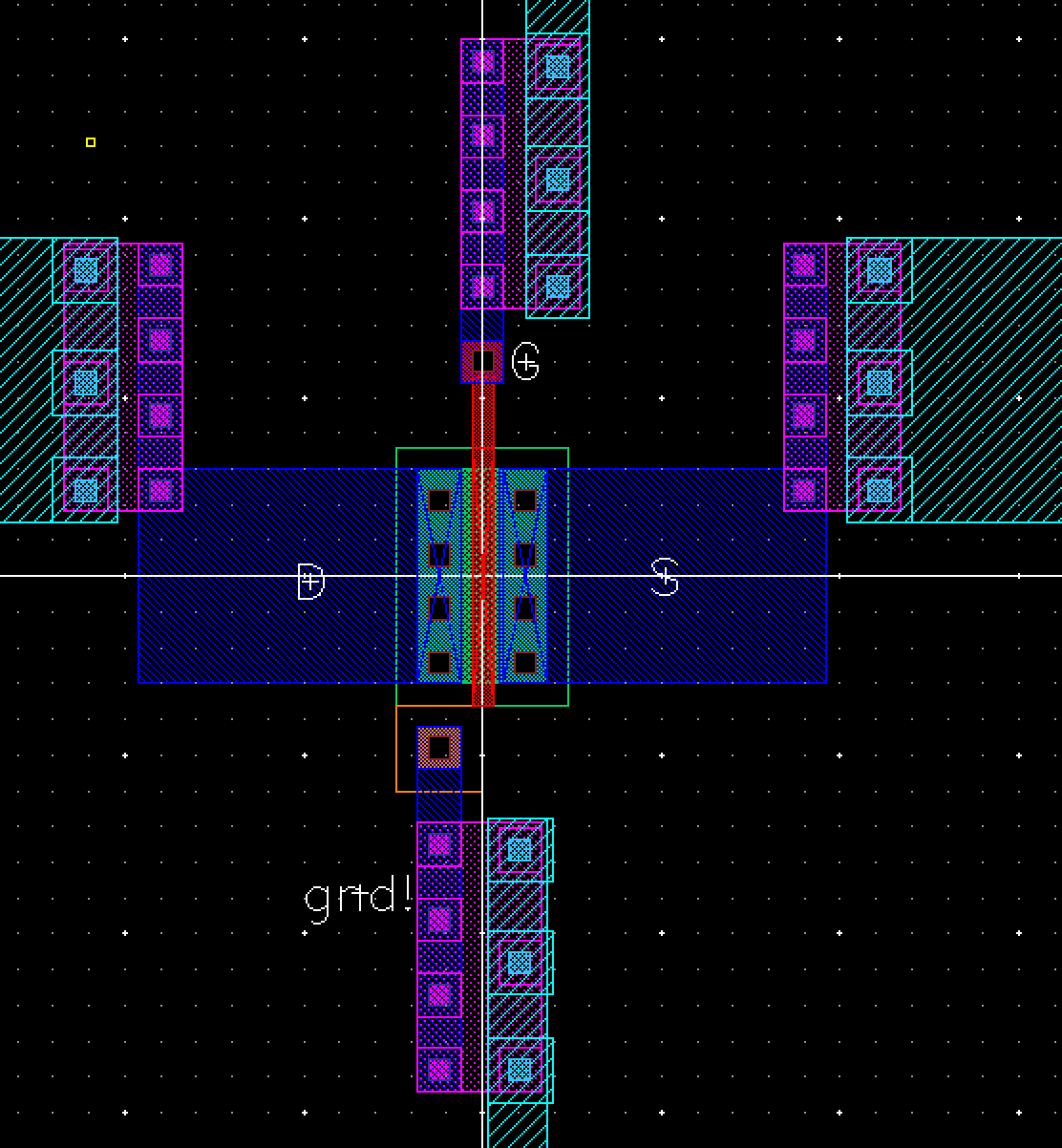
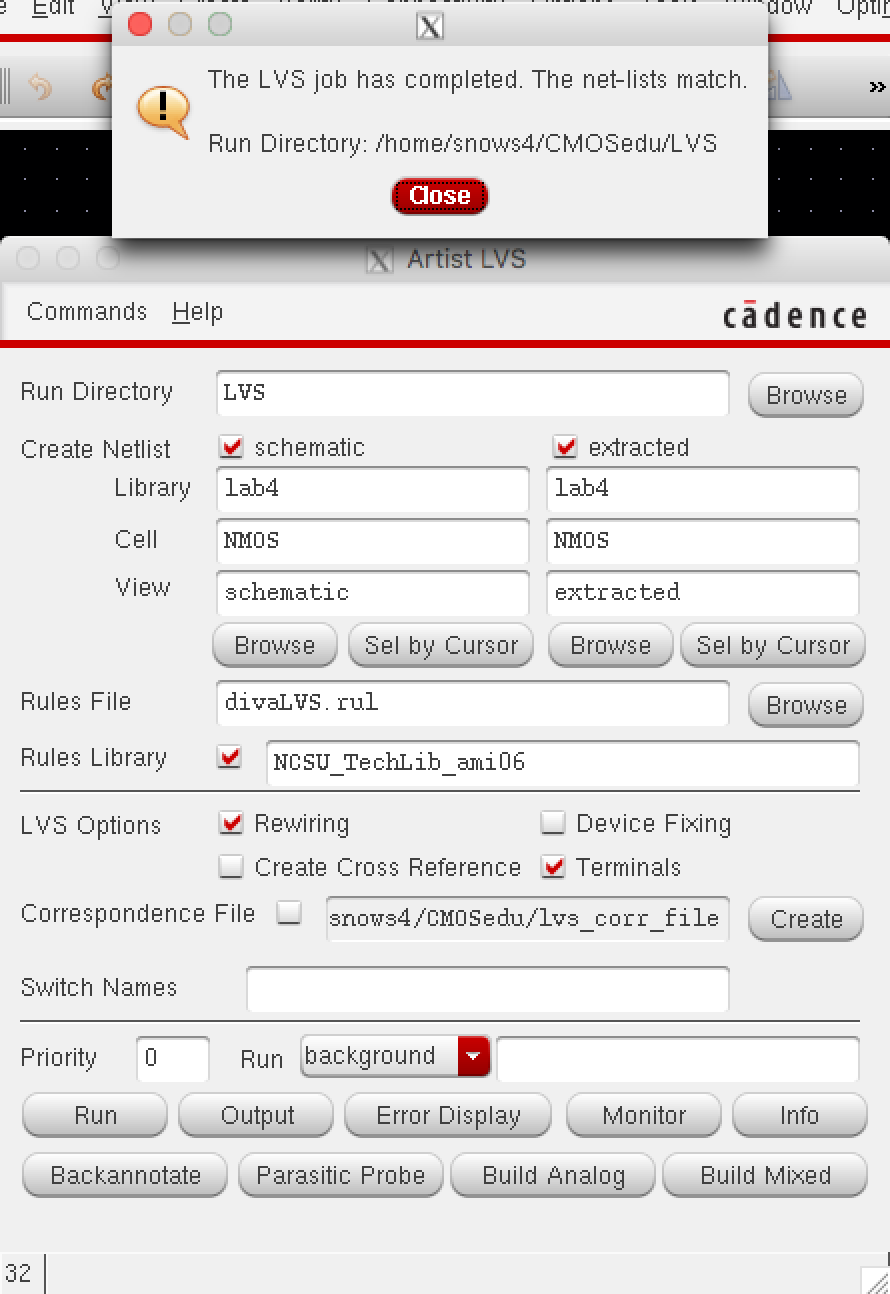
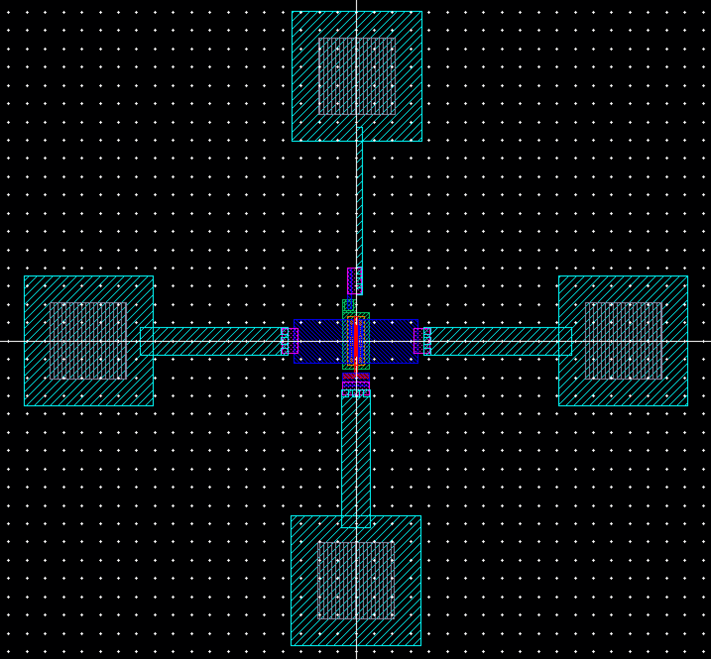
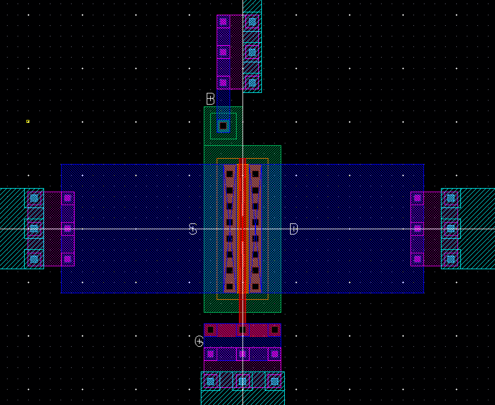
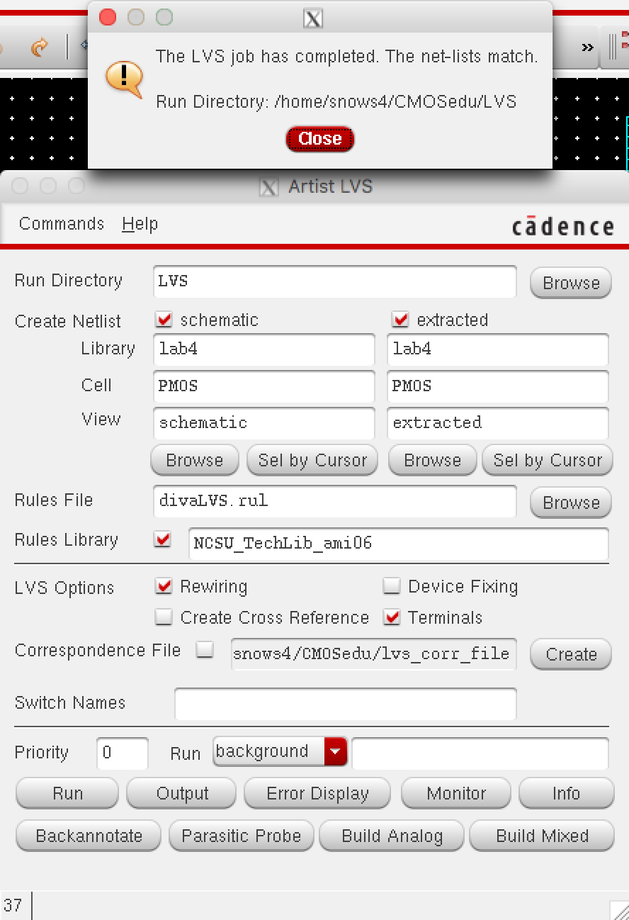
Following the prelab instructions, I backed up my work completed Tutorial 2.
Lab:
We began the lab by generating a schematic for a NMOS device with a 6u/600n width-to-length ratio.

I used this schematic to make the symbol used for simulating the NMOS.
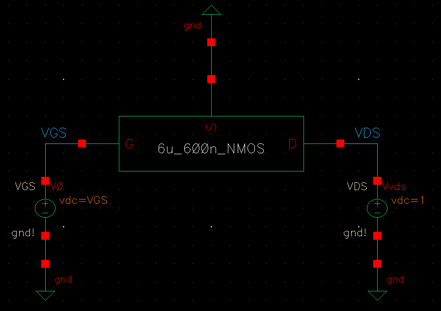
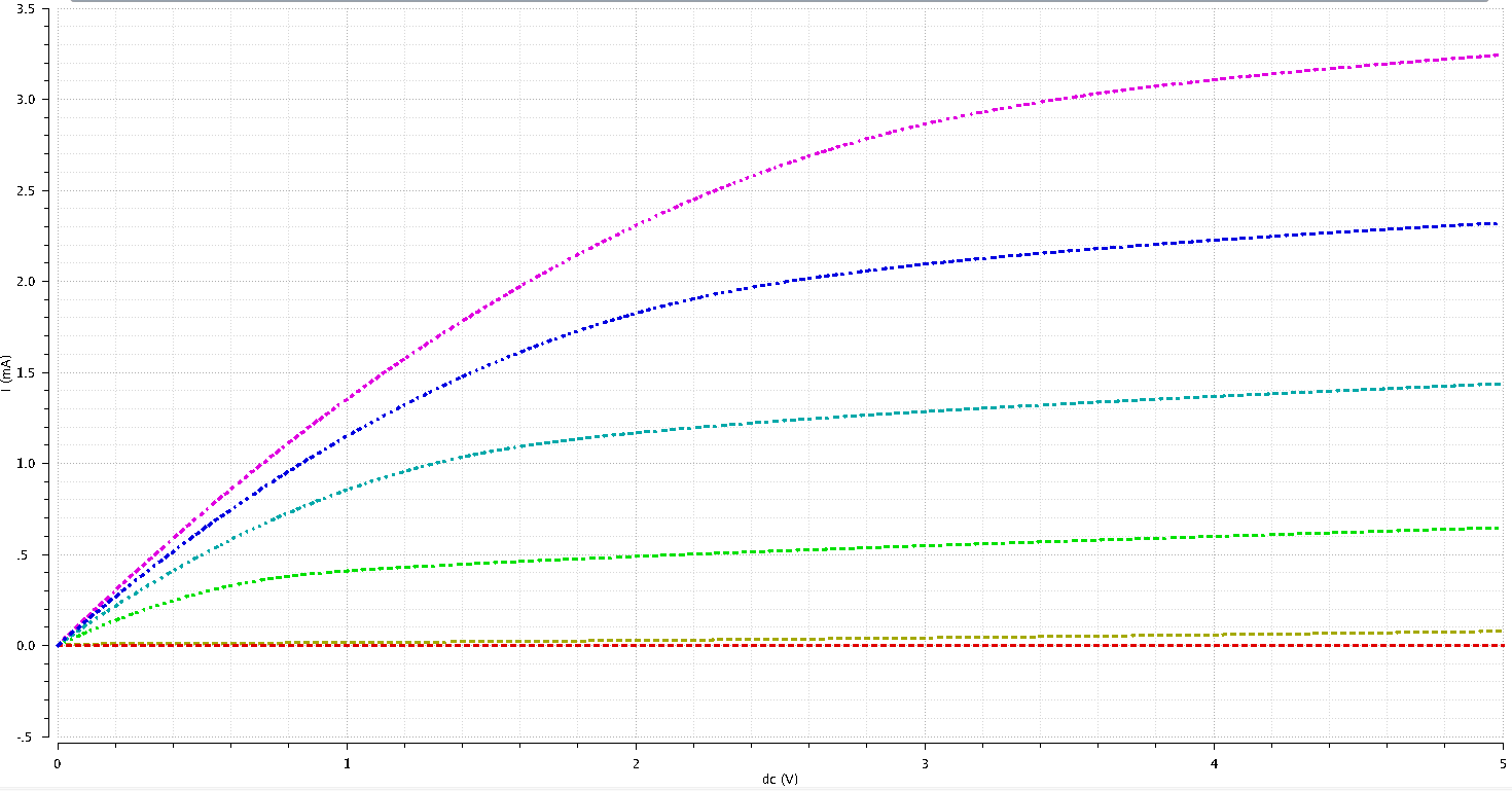
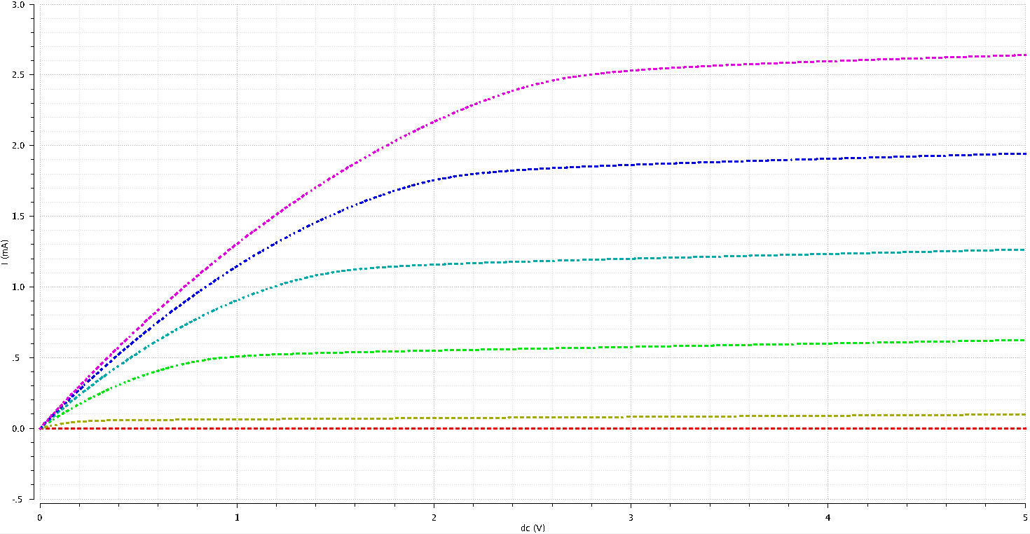
I configured the ADE L to graph ID vs VDS while carying VGS from 0v to 5v in 1V steps while varying VDS from 0v to 5V in 1mV steps.

That produced the following relationship:
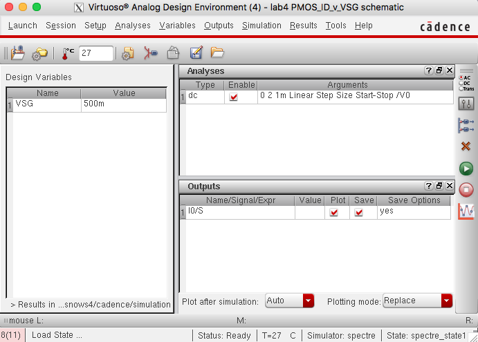
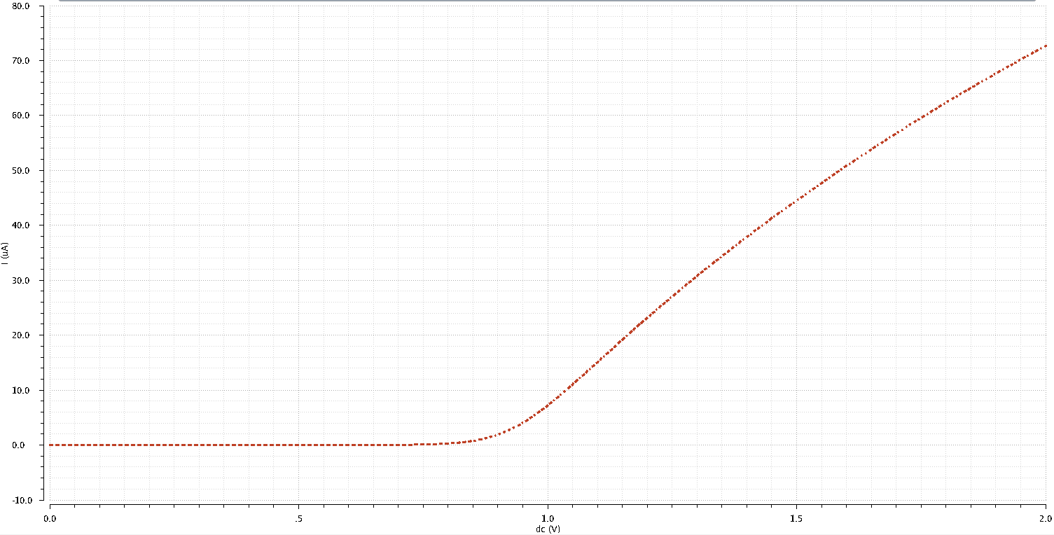
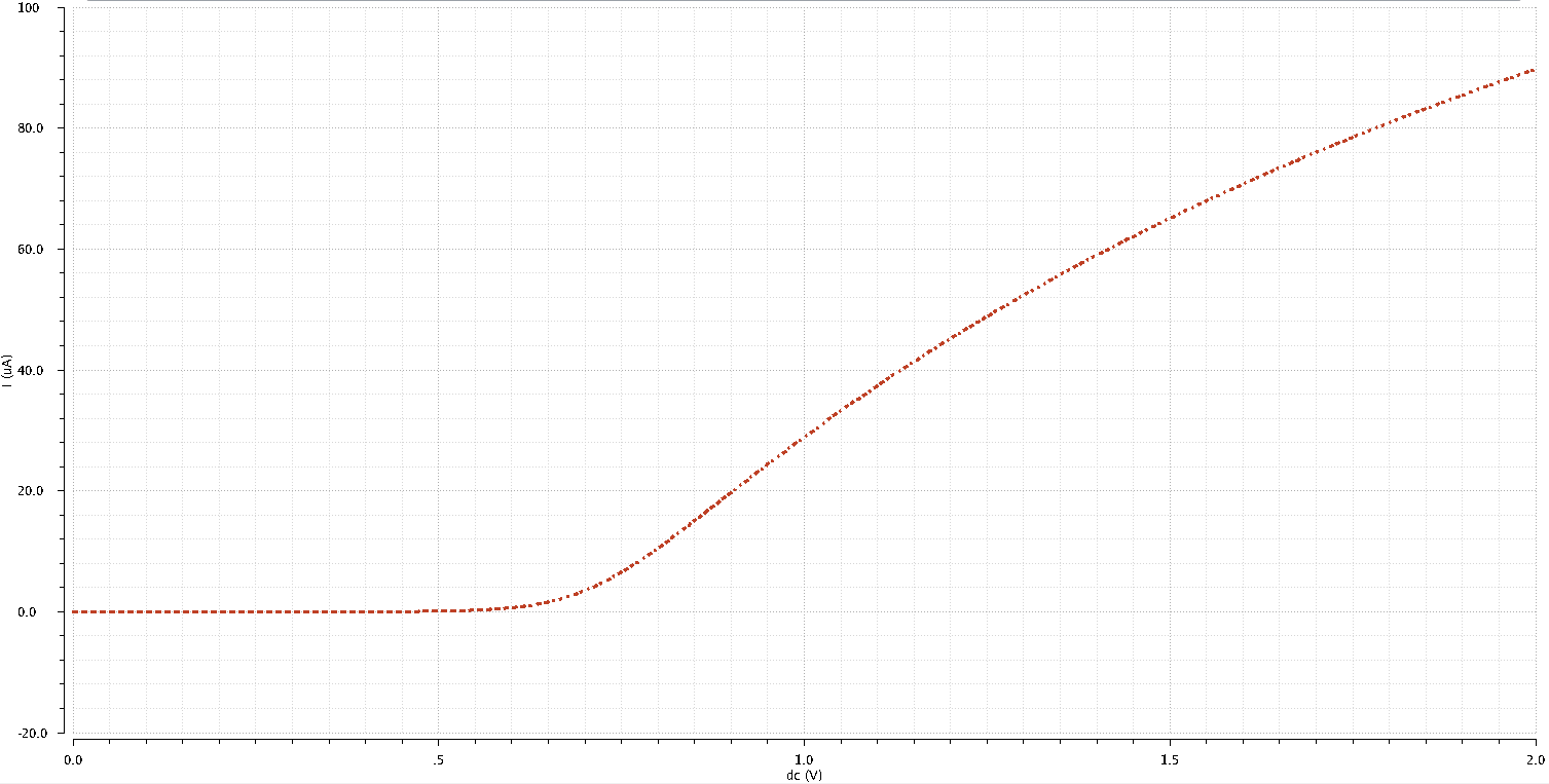
I then configured the ADE L to graph ID vs VGS while varying VGS from 0V to 2V in 1mV steps while VDS is set to 100mV.
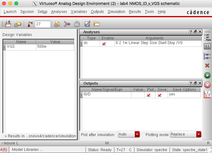
Which produce the this relationship:
I next generated the schematic for a PMOS device with a 12u/600n width-to-lenght ratio.

I used that schematic to create the symbol I used in the following PMOS simulation circuit.
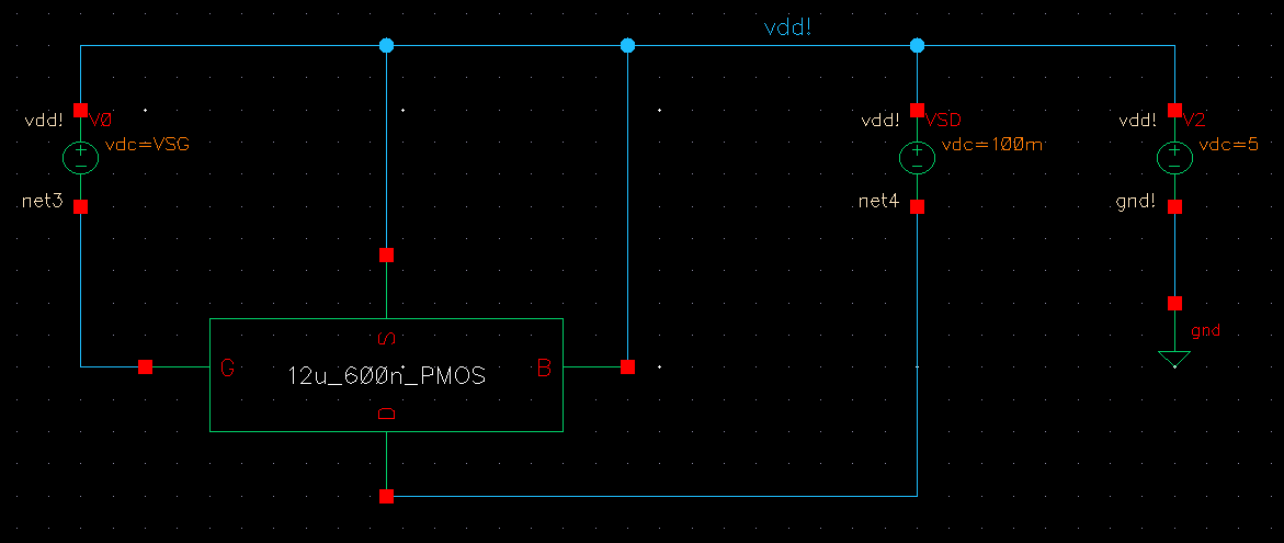
I next configured the ADE L to plot ID vs VSD while varying VSG from 0V to 5V in 1V steps and varying VSD from 0V to 5V in 1mV steps.

That provided the following graphical representation:
