Lab 6 - EE 421L
For the Pre-Lab, we needed to go through Tutorial 4
in preparation for this lab. In the tutorial, a NAND gate is
created using NMOS and PMOS and then tested out.
Creating a 2-input NAND gate
First, a schematic of the 2-input NAND gate, shown below, is created using NMOS and PMOS that both have a width of 6um and a length of 600nm. Pin A and Pin B are representation of the two inputs in the NAND gate and the Pin AnandB are the representation of the output of the NAND gate. Once the schematic has no error when it's checked and saved, a symbol is created as shown below.
Symbol

| Layout | Extracted |
 |  |

Creating a 2-input XOR gate
First,
create the schematic of an XOR gate, as shown below, using again NMOS
and PMOS that are both 6um wide and 600nm long. Pin A and Pin B are representation of the two inputs in the XOR gate and the Pin AxorB
are the representation of the output of the XOR gate. Once the
schematic has no error when it's checked and saved, a symbol is created
as shown below.
Schematic

Symbol

Next,
a layout of the XOR, shown below, is created by instantiating six nmos
and six pmos, where there are two sets of each of the PMOS and NMOS are
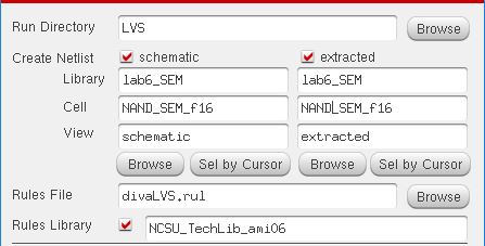
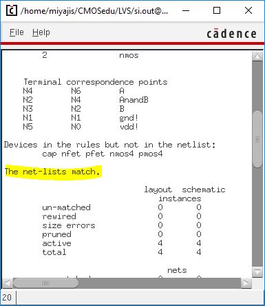
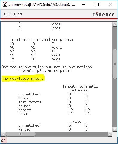
overlapped and flattened. Again, the metal1 and cc's of the NMOS in the middle are deleted. Once everything is connected and labeled, DRC the layout, extract it, and LVS it.
| Layout | Extracted |
 |  |
DRC

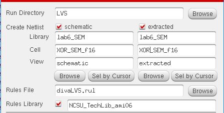
LVS
Gate Simulation
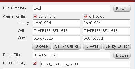
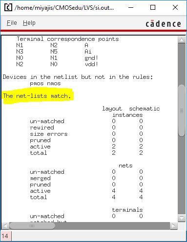
Before any simulation is done, an inverter, shown below, must be created with an NMOS and a PMOS, where they both have a width of 6um and length of 600nm. Once the schematic, symbol, and layout of the inverter passes, we are ready to do the gate simulation.
Inverter Schematic

Inverter Symbol

| Layout | Extracted |
 |  |

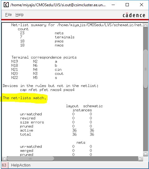
LVS
Schematic

Simulation

| A | B | Ai | AnandB | AxorB |
| 0 | 0 | 1 | 1 | 0 |
| 0 | 1 | 1 | 1 | 1 |
| 1 | 0 | 0 | 1 | 1 |
| 1 | 1 | 0 | 0 | 0 |
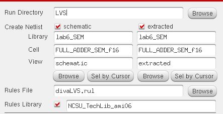
Creating and Testing the Full Adder
First, a schematic of the full adder, shown below, is created by instantiating the symbols of the NAND and XOR gates that were created earlier. After checking and saving the schematic, create a symbol as a representation of a full adder to be used for simulation.
Schematic

Symbol


Schematic

Simulation

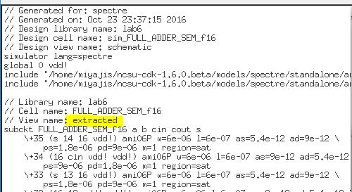
Simulation Netlist
Truth Table
| a | b | cin | s | cout |
| 0 | 0 | 0 | 0 | 0 |
| 0 | 0 | 1 | 1 | 0 |
| 0 | 1 | 0 | 1 | 0 |
| 0 | 1 | 1 | 0 | 1 |
| 1 | 0 | 0 | 1 | 0 |
| 1 | 0 | 1 | 0 | 1 |
| 1 | 1 | 0 | 0 | 1 |
| 1 | 1 | 1 | 1 | 1 |
Again,
there are glitches due to the voltage dropping and rising
around the same time. If you look closely, the fall time of one
input voltage is at different time from the rise time of another
input voltage; therefore, causing the simulation to drop and rise
within a very short period of time.
Here is lab 6 files: lab6.zip
Back-Ups
Backing up my lab content in both my student drive and Google drive.