Lab 5 - EE 421L
Creating a 12u/6u Inverter
Convert the schematic into a symbol and use note (shift + N) to keep track of the widths of the PMOS and NMOS.
Symbol

Layout and Extracted Layout


Creating a 48u/24u inverter
Since the same schematic as the 12u/6u inverter is being used for the 48u/24u inverter, the file of the 12u/6u inverter can be copied and renamed. When the file is copied over, change the multiplier of both the NMOS and PMOS from 1 to 4. Once that is done, Check and Save the schematic.
Schematic

Again, convert the schematic into a symbol and use note (shift + N) to keep track of the widths of the PMOS and NMOS.
Symbol

Create a layout with an ntap, ptap, m1_poly, pmos, and nmos. The size and multipliers of the NMOS and PMOS are the same as the ones in the schematic. Then connect each of the poly layers of the NMOS and PMOS that are adjacent to each other. Connect the second and fourth metal1 layer of the NMOS and PMOS together. Connect the first, third, and fifth metal1 of the NMOS to the metal1 of the ntap, and again with the PMOS except it is connected to the ptap. The m1_poly is connected to all of the poly rectangles using the poly layer. Lastly, add metal1 pins to the ntap as vdd!, ptap as gnd!, m1_poly as pin A, and path between the NMOS and PMOS as Ai. Then DRC the layout, extract it, and LVS the schematic and extracted layout of the inverter.
Layout and Extracted Layout


DRC and LVS


Simulations with Different Loads
Using a 12u/6u inverter:
| Capacitor Load Value | Schematic | Simulation |
| 100fF | 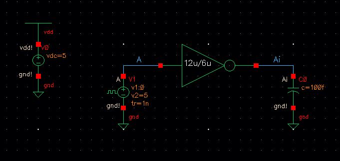 |  |
| 1pF | 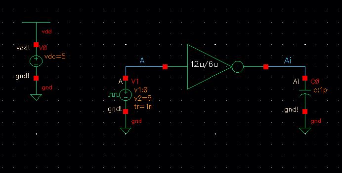 | 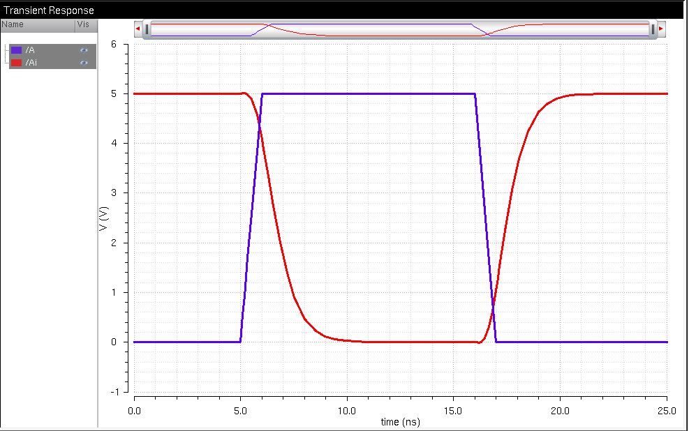 |
| 10pF | 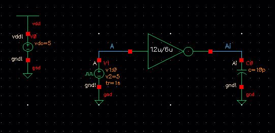 | 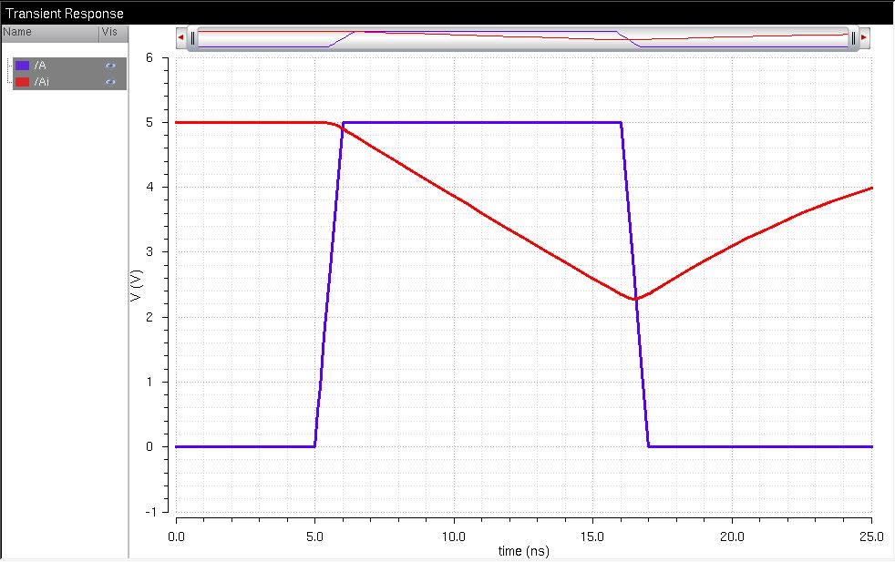 |
| 100pF | 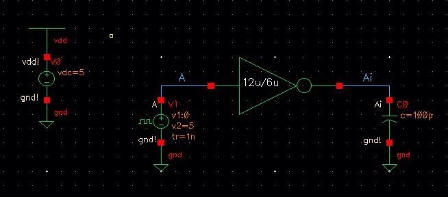 | 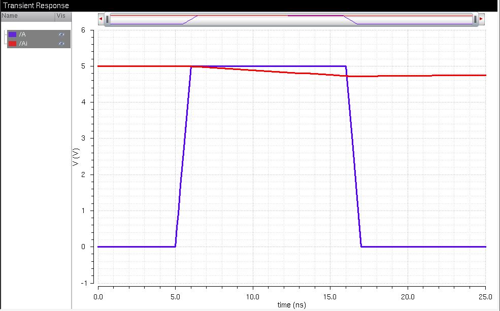 |
Using a 48u/24u inverter:
| Capacitor Load Value | Schematic | Simulation |
| 100fF | 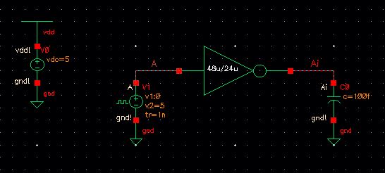 | 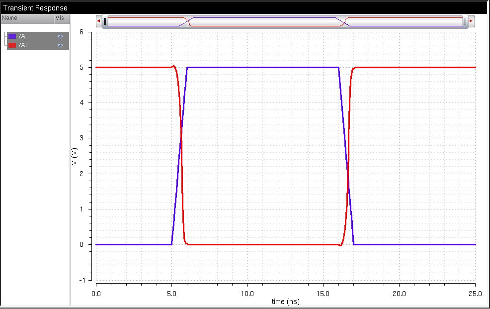 |
| 1pF | 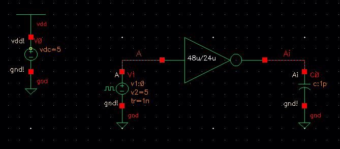 | 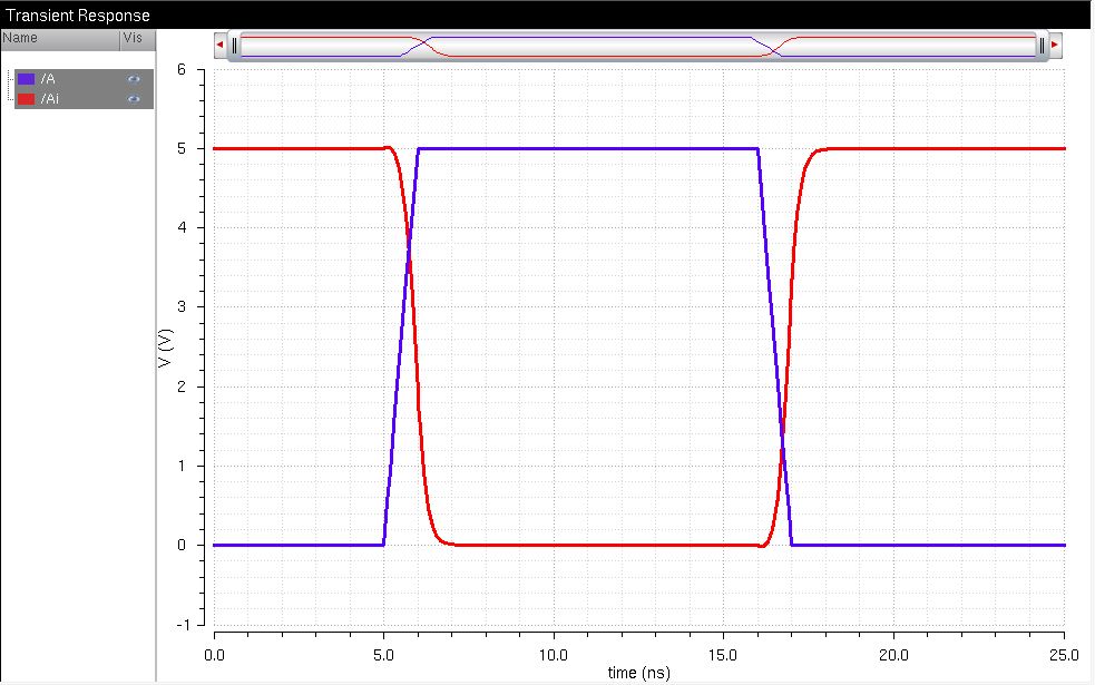 |
| 10pF | 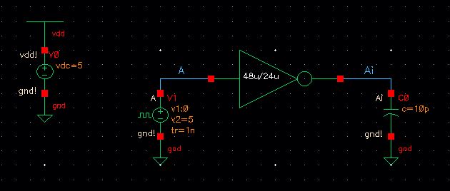 | 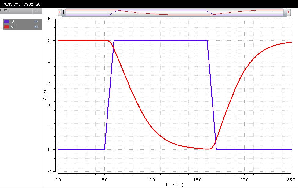 |
| 100pF | 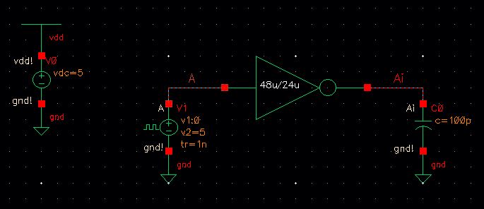 | 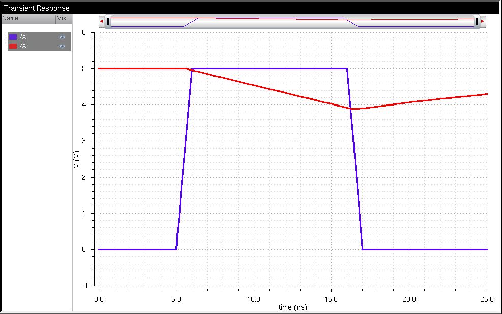 |
Based on the simulations above, the time delay increases as the value of the capacitor increases. When the inverter is multiplied by 4, the time delay of the simulations are shorter than the ones with the inverter multiplied by 1. The larger inverter is faster because the resistance is smaller causing it to charge and discharge faster; therefore, there is more current flowing in, flowing out, and being stored.
UltraSimulations
Again, simulate the schematics above, except change the simulator to UltraSim in the Choosing Simulator/Directory/Host instead of Spectre. UltraSim simulates the schematic faster.
Using 12u/6u inverter:
| Capacitor Load Value | Simulation |
| 100fF | 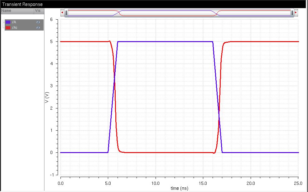 |
| 1pF | 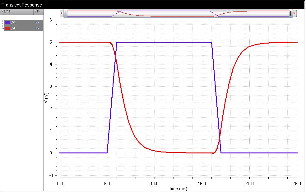 |
| 10pF | 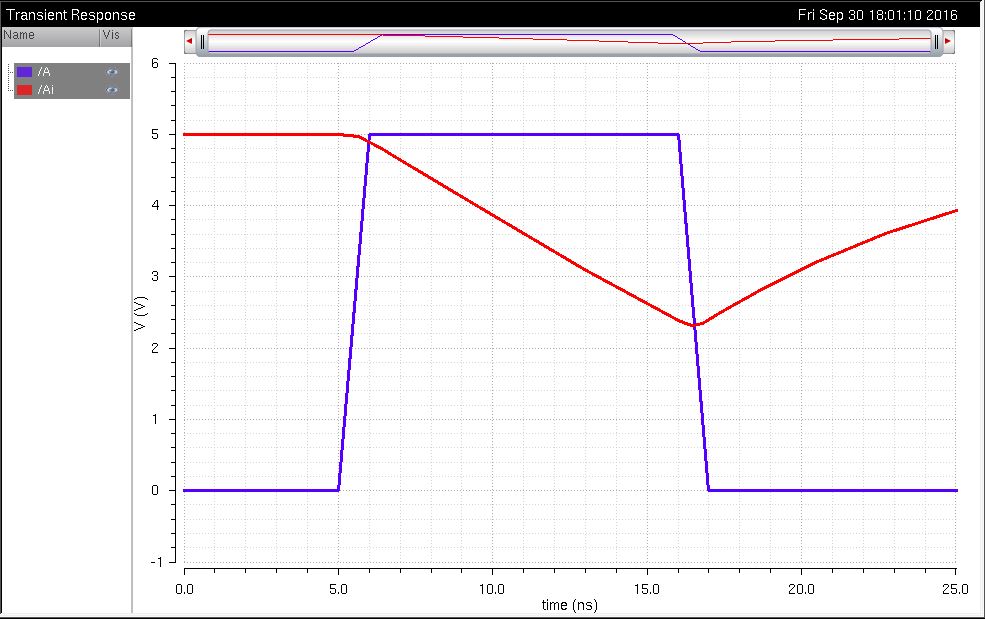 |
| 100pF | 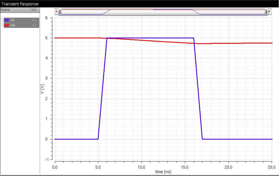 |
Using 48u/24u inverter:
| Capacitor Load Value | Simulation |
| 100fF |  |
| 1pF | 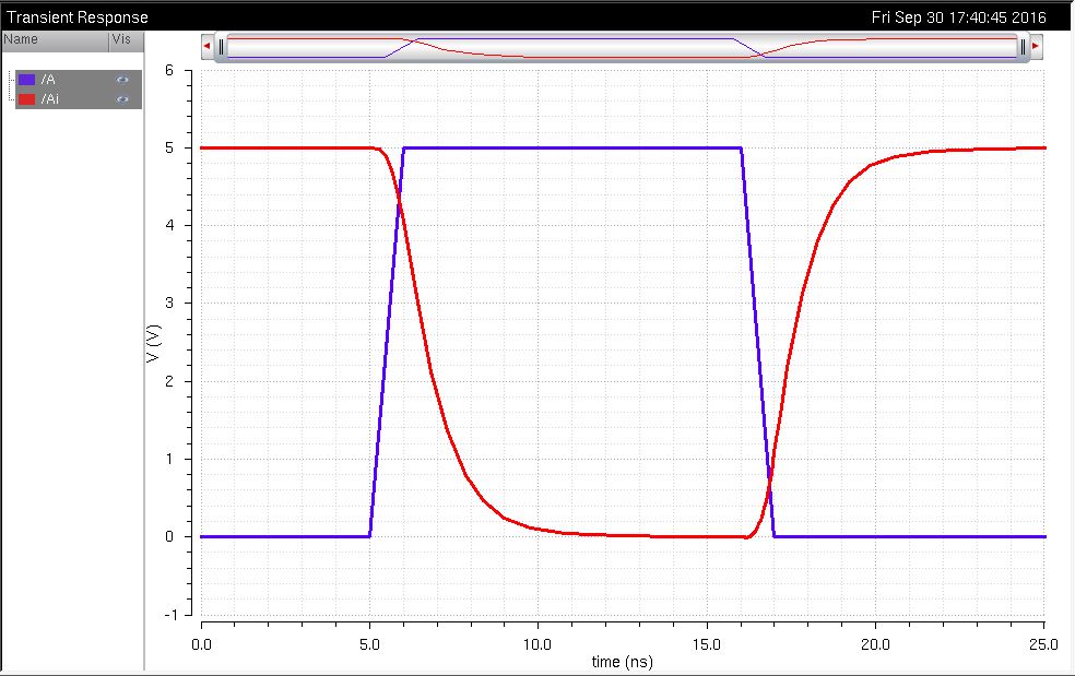 |
| 10pF | 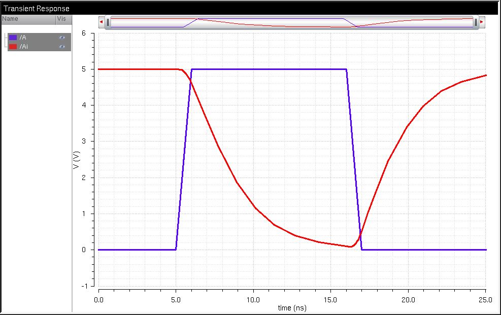 |
| 100pF | 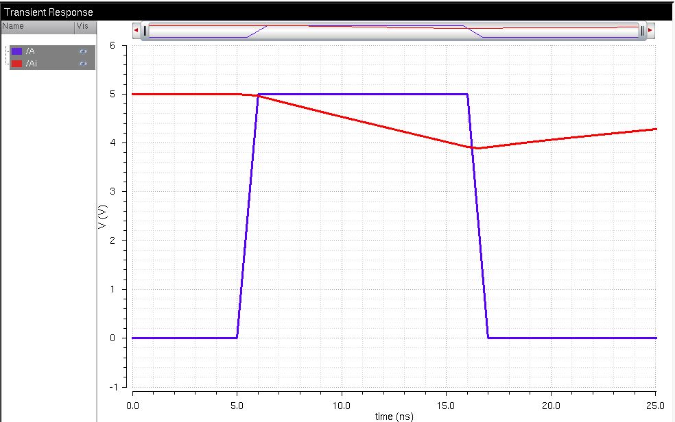 |
The results of the simulations in both spectre and ultrasim simulator setting are very similar to each other.
Here is the lab5 zip file: lab5.zip