Lab 4 - EE 421L
NMOS
| Layout | Schematic | Symbol |
| | |
PMOS
| Layout | Schematic | Symbol |
 |  |  |
Simulations
1. Using the symbol of the NMOS (6u/600n) that was created in the prelab (Tutorial 2), we connect the source of the NMOS to ground, the gate of the NMOS to a voltage source of VGS, and the drain of the NMOS to separate voltage source of 1 volts to plot an ID vs. VDS curve of an NMOS device. The VGS is set from 0 to 5 volts in 1 volts steps and VDS is varying from 0 to 5 volts in 1 mV steps. Before plotting the IV curve, select the drain current for the simulations. In the simulation, each of the lines represents the drain current at the different voltage from the drain to the source starting at 0 volts to 5 volts.


2. To plot an ID vs. VGS curve of an NMOS (6u/600n) device, the same schematic is used as the ID vs. VDS, but VDS is changed to 100 mV instead of 1 volts and VGS will be varying from 0 to 2 volts in 1 mV steps. In the simulation, VGS is greater than the threshold voltage, which causes the current to rise.


4. To plot a ID vs. VSG curve of a PMOS device (12u/600n), the same schematic previously is used, except VSD is set to 100 mV and VSG is varying from 0 to 2 volts in 1 mV steps. The simulation is a representation of the amount of VSG needed in order for the drain current to rise.


NMOS Device with Probe Pads
Before
attaching the probe pads to the NMOS device, the NMOS created earlier
must be modified to where the body of is a pin instead of it being
connected to ground. Once those changes are made, then the attach
a probe pad to each of the terminals in the NMOS device in layout and
schematic as shown below.
Layout

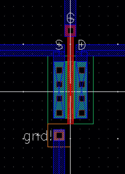
NMOS Zoomed In
Schematic
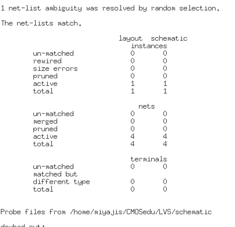
Once both the layout and schematic are created, DRC extract the layout, and LVS the extracted layout and schematic.
DRC
LVS
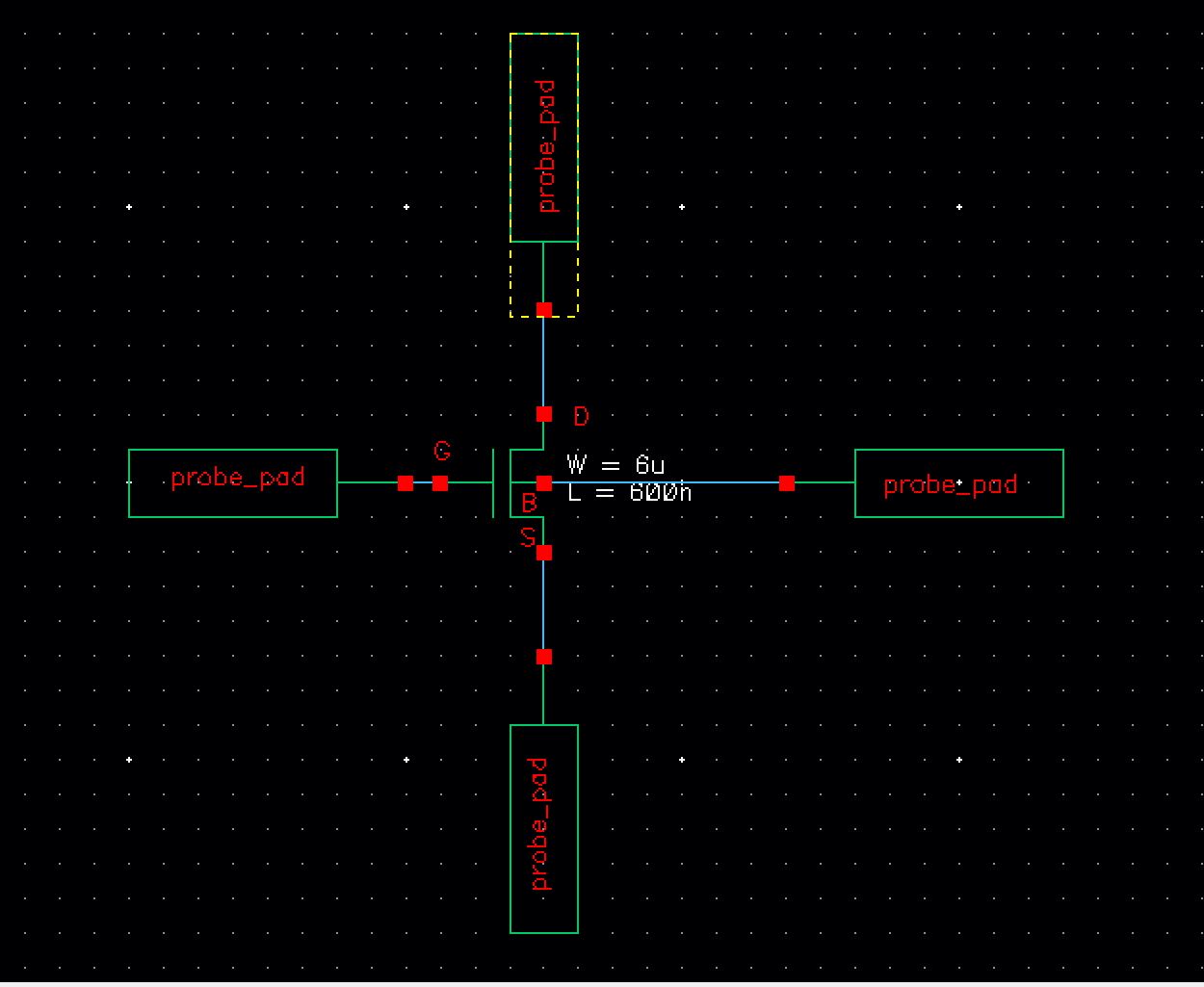
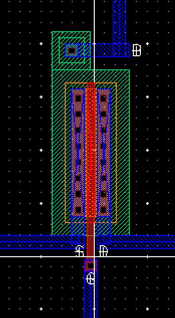
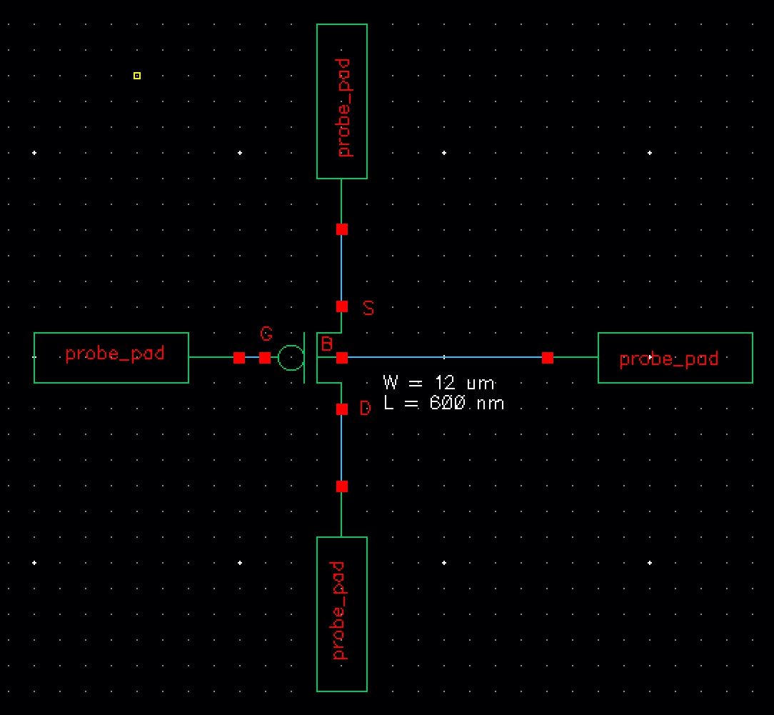
PMOS device with Probe Pads
Using the PMOS created earlier, connect each terminal in the PMOS device to a probe pad in both the layout and schematic.
Layout
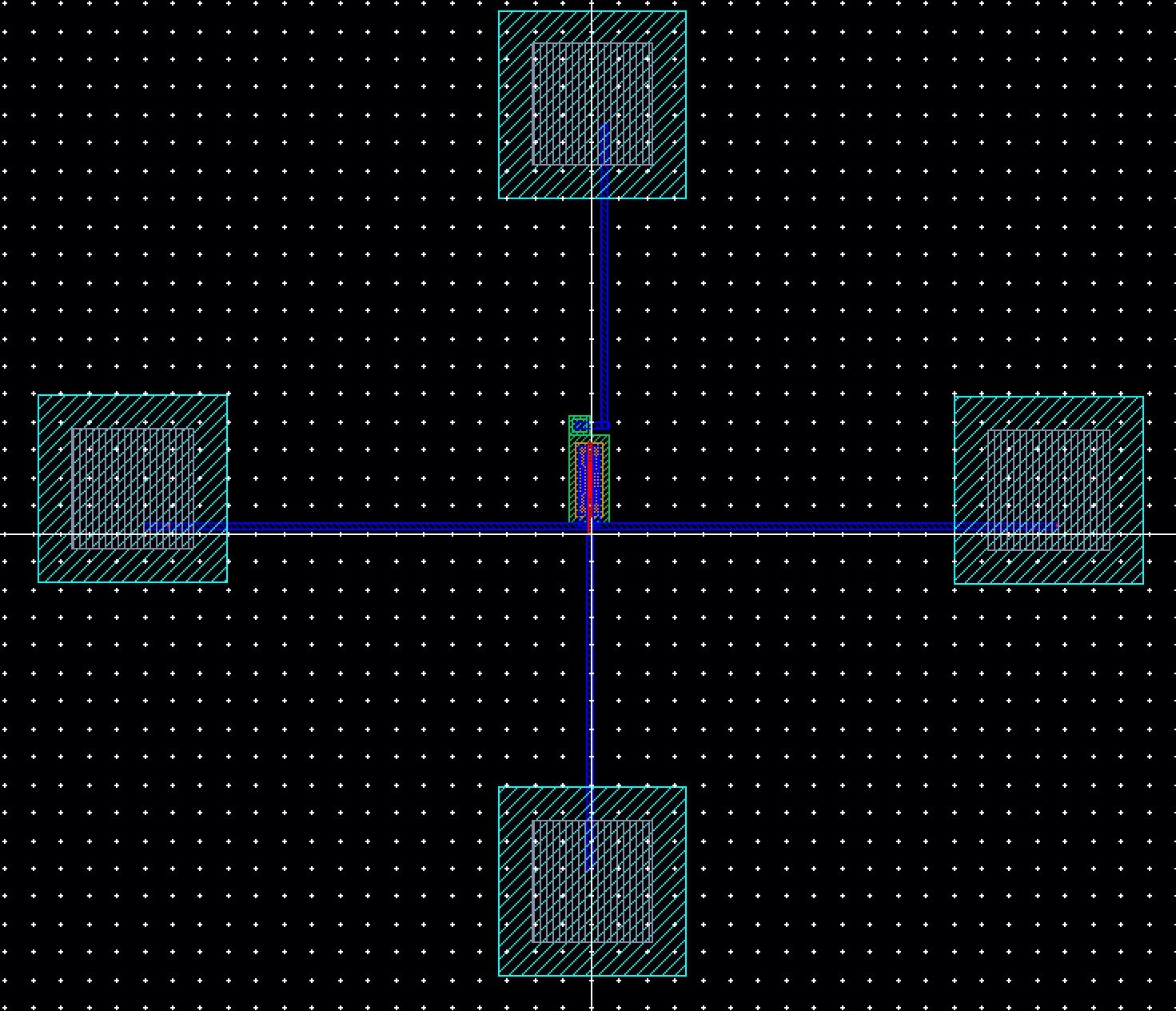
PMOS Zoomed In
Schematic
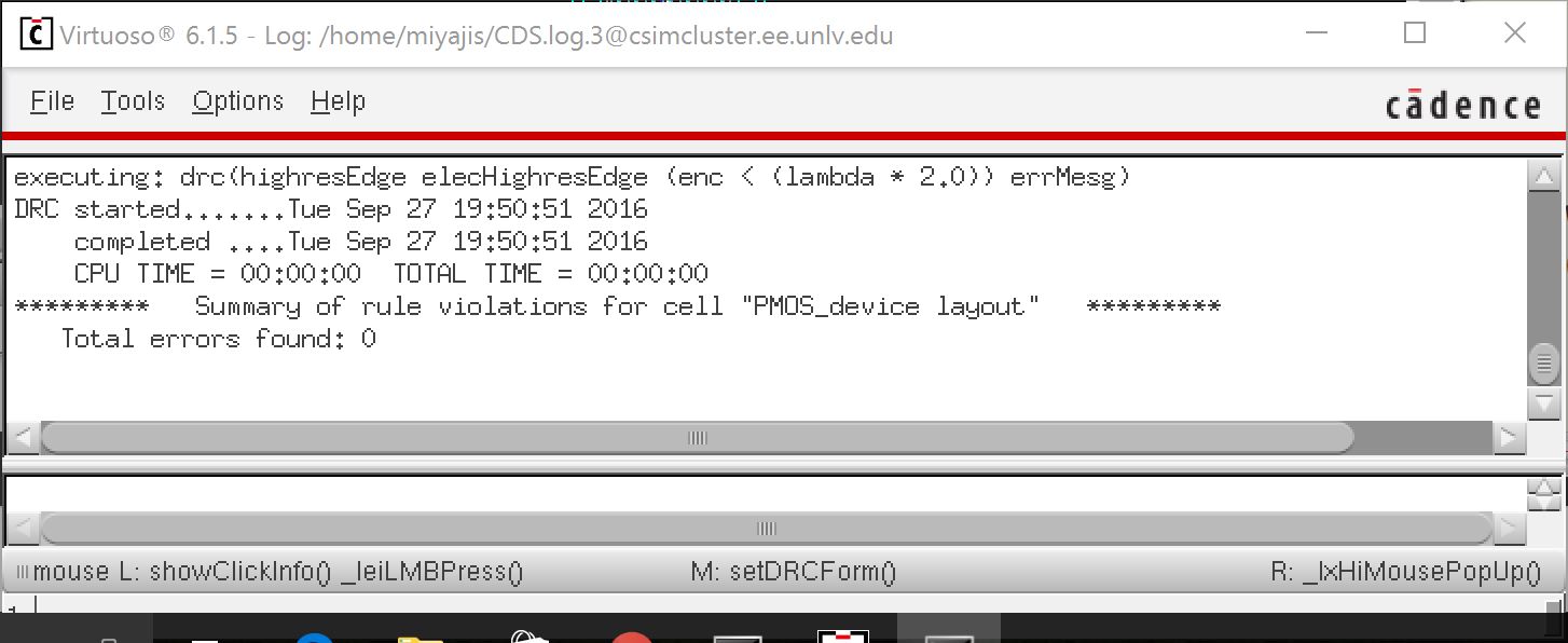
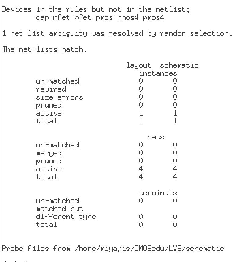
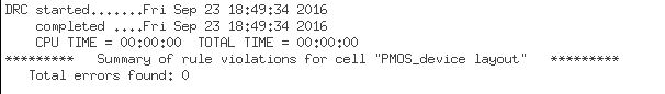
Once the layout and schematic are created, DRC and extract the layout and LVS the schematic and extracted layout.
DRC
LVS