Lab 3 - EE 421L
Lab Work:
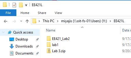
The purpose of Lab 3 is to be able to create a layout of the 10-bit DAC that was built in Lab 2 and simulate its extracted version. Since we need the 10-bit DAC that was created in Lab 2, right click on Lab 2 and copy it as Lab 3, so we can edit it.
Designing a Layout of a 10k Resistor
In
Lab 2, 10k resistors were used in the schemtic of the 10-bit DAC, so
the same value resistor needs to be created in the layout. In
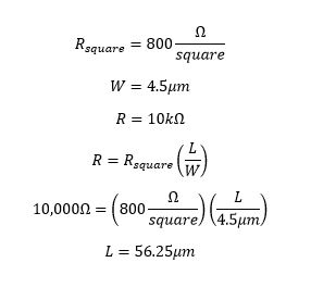
order to figure out the dimensions, the equation and assumptions below
are used. According to MOSIS, the sheet resistance is 800
ohms/square. Also the width of the n-tap that are attached to
each end of the n-well is 4.5 microns; therefore, the length of the
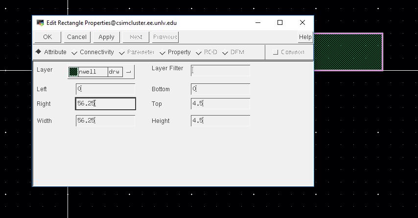
n-well is 56.25 microns. In the layout window of the 10k
resistor, select the n-well layer on the left side and hit bindkey r
to create a rectangle of the n-well. Left and right refers to the
length of the n-well and bottom and top refers to the height of the
n-well.
Once the n-well rectangle is set, n-taps are added to each side of the rectangle. They must be touching the n-well in order for it to pass the DRC. Metal1 pins are added in the n-tap metal1 layer. Lastly, the resistance sheet is added on top of the n-well rectangle by selecting the res_id layer and click on bindkey r. Then save and DRC the layout to see if it passes. If it passes, then extract the layout to see if the n-well resistor is close to 10k.
Layout of 10k resistor:

Extracted file of 10k resistor:


Creating a DAC Layout Using 10k N-well Resistors
Under the DAC that was created and copied from the previous lab, create a new layout and instantiate the 10k resistor that was just made into your layout five times directly above each other with space in between. One pin of the bottom resistor must be connected to ground, so a metal1 layered pin is created and labeled gnd!. On the other side of the same resistor, a metal1 rectangle is connected to one pin of the resistor above it to make them in series. This process is done two more times, so there should be four resistors in series with each other. After connecting the four resistor in series, create another metal1 pin on the opposite and label it B0 to represent to the bit number in the DAC. To create another bit, the fifth resistor must be in parallel by making a metal1 path (bindkey p) starting from the metal1 rectangle in between the second and third resistor to the fifth resistor pin as shown below. DRC the layout to make sure there are no errors before continuing. If there are any errors, it may be because the distance between the resistors and metals are too small.

This process is repeated 9 more times to make it a 10-bit DAC, but without the resistor that is connected to ground as shown above. As a short cut, highlight the top three resistors with the metal1 paths and rectangles and click bindkey c. After copying the bits, change the bit label to the correct number. The final layout should look similar as the image below.


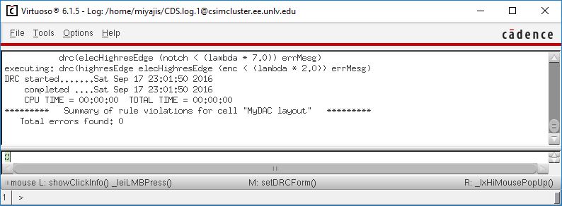
When everything is finished, DRC the layout again to make sure there are no errors in the design by looking at the Cadence command window as shown below.
If the design passes, extract the layout and it should look similar to the picture below.
Extracted layout from B5 to B9


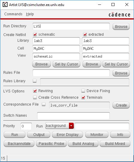
Next, the schematic and extracted layout of the 10-bit DAC has to be LVS to make sure they are the same. To LVS the DAC schematic and extracted layout, click on the Verify tab and select LVS. A window, like below, should pop up. Browse to the schematic of your 10-bit DAC on the left side and the extracted layout of your 10-bit DAC on the right side. Click on Run and then Output to see if the netlist matched.
LVS window
LVS Output Window

Simulations with the Extracted Layout
Using the same schematics as we used in Lab 2, we will apply the extracted layout instead of the schematic of the 10-bit DAC created. In order to do that, we open up the ADE L window of the schematic that you would like to simulate and Load State to Cellview. Then click on the Setup tab and select Environment. In the Switch View List, type in extracted before the word schematic, like below, click OK, and run the simulation.

To make the simulation is using the extracted layout, click on the Simulation tab, Netlist, and Display in the ADE L window.

| Description | Schematic Simulation | Extracted Simulation |
| This is the simulation of your own DAC connected to the ADC with no load added. There is not too much of a difference between the two simulations. In the schematic and extracted simulations, the input voltage is close to the values of the output voltage. |  |  |
| This is a simulation of finding the delay of the DAC created. All of the pins in the DAC created is connected to ground, except for pin B9. B9 is attached to the voltage source with a pulse from 0 to 5 volts. The output voltage source pin is connected to a 10pF load. The schematic simulation is slightly different from the extracted simulation. |  |  |
| This is the simulation with the DAC attached to the ADC with a 10k ohm load attached to the output voltage. Again, there is not too much of a difference between the two simulations. |  | 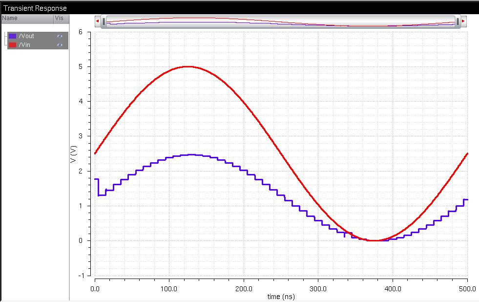 |
| This is the simulation with the DAC attached to the ADC with a 10pF load attached to the output voltage. There was not too much of a change between the two simulations. |  |  |
| This is the simulation with the DAC attached to the ADC with a 10pF and 10k ohm load attached to the output voltage pin. Again, there was not too much of a difference between the two simulations. |  |  |
Overall, when simulating either the schematic version or extracted layout of the 10-bit DAC, there is not too much of a difference in the simulations. If you look very closely, the difference is very small since the resistor values are not exactly the same.
Here is the attachment to my Lab 3 Cadence Files: lab3.zip
Back Up