Lab 7 - ECE 421L
Cassandra Williams
Willi131@unlv.nevada.edu
October 19, 2015
PreLab:
For this prelab 7we went through Tutorial 5 for the cadence design system from CMOSedu.com.
There we constructed schematics, simulated, and then did the
layouts for a ring oscillator using our inverter created in a previous lab.
I. Ring Oscillator
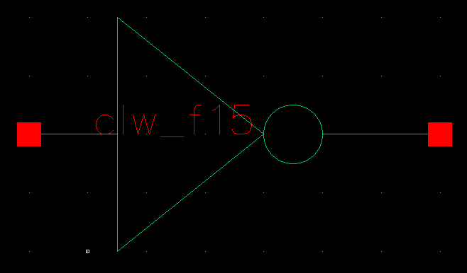
First, copying the inverter symbol file created in the previous
tutorial, we created a new schematic instantiating our inverter.
Then copying the and hitting F3 (opening a special options box),
we modified the columns to 30, which will give us our 31 stage ring
oscillator...

Above
is our resulting ring oscillator schematic: You can see that the output
on the end is wired back to the input of the very first inverter in our
line, creating the ring.
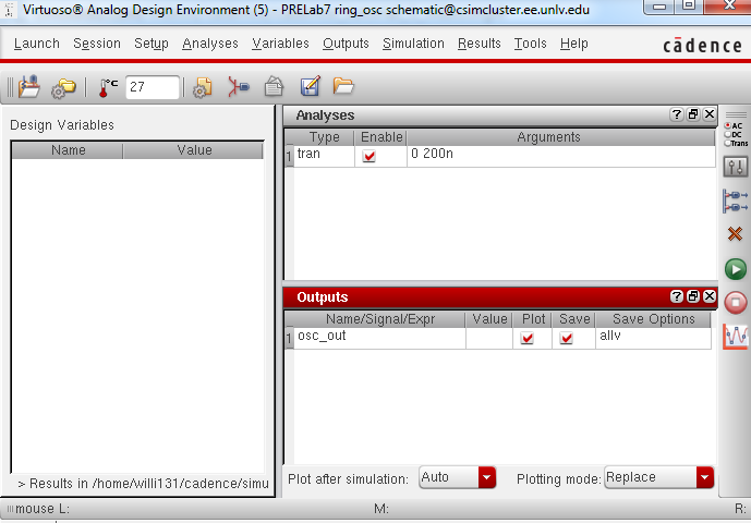
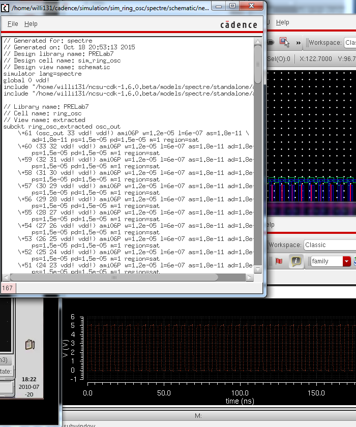
Next, after
checking and saving with no errors, it's time to run an analysis to see
the ring's behavior. Opening the ADE L, we have to
remember to set the MOSFET libraries, and then make sure we set our vdd
to 5V. Also, we had to set our intial conditions for our osc_out
node to zero. (Otherwise we don't get the oscillation we want and
instead the output is a steady voltage or around 2.5V) So now we do our
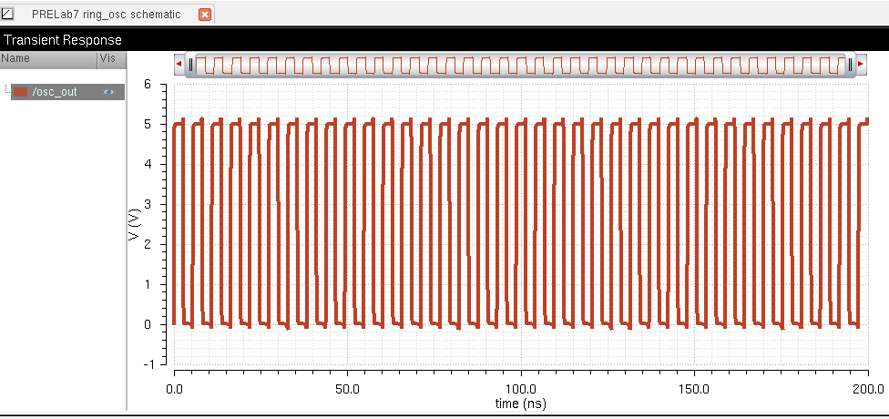
transient length of 200ns and below is our results:
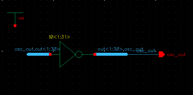
II. Ring Oscillator Array
Now, to simplify our circuit a bit we deleted all the added
inverters leaving just our original again. Now, We hit the bind
key 'Q' and change our instance name to IO<1:31> and turn the
display to Value. This is creating our 31 inverters for our ring
oscillator using an array. Below you can see this:
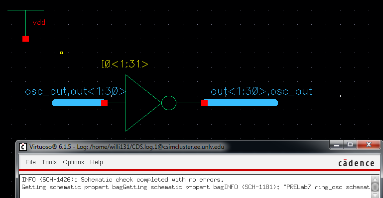
For
our input and output we create wide wires/busses to connect to our
array. Here the wire names are: Input-->
osc_out,out<1:30> and our output-->
out<1:30>,osc_out... This is naming the wires in such a way that
input of the first inverter is osc_out and its output is out<1>,
then the next inverter's input is out<1> and its output is
out<2>, and so forth until the last inverter is reached, then its
output is then osc_out. Here, the assignments declare the loop
connection while keeping the schematic neat.
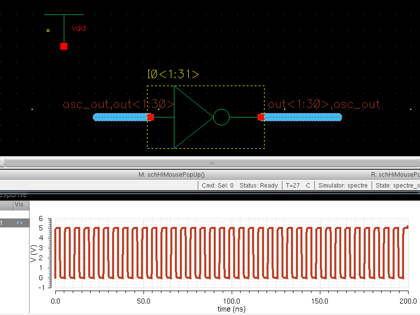
Next,
we run the simulation on our new schematic. The state was saved
and can just be reloaded for this sim... Below is the results.
Here you can see that they are the same as our original.
This should indeed be the case as they are the same schematic!
III. Layout
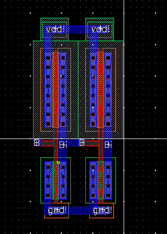
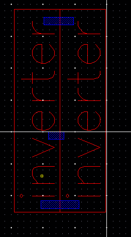
Next, we create a layout for the ring oscillator. First we
instantiate two inverters into the layout right next to each other.
Then we create connections between each of the inverter's vdd!,
gnd!, and in/output. Then, taking it to 0-level display we can
see how they are connected.
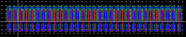
After we ensure that the above successfully DRC's, we delete the
second invertoer. Then we copy the first and hit F3 again just as
before to create our array of 30 columns... After placing the
inverters end to end and making sure they're all connected properly
(with our premeasured metal 1 connections from before), we DRC our
layout.
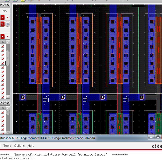
Next, we add our pins for our in/outputs to match our schematic (vdd!,
osc_out, and gnd!). After the DRC is successful with no errors we
extract the layout.
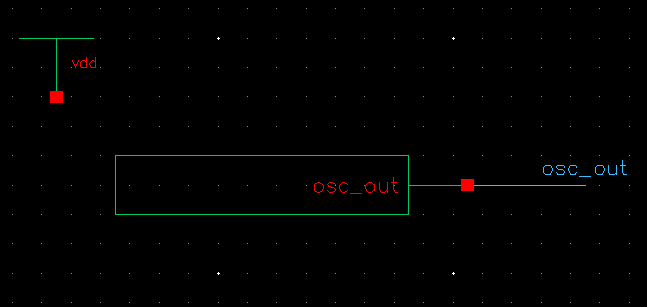
IV. Oscillator Ring Symbol
Now, we create a symbol of our oscillator ring. Below you
can see our symbol instantiated into a new schematic to use for
simulation and testing.
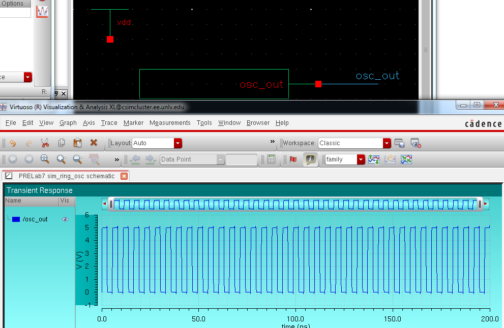
Here
are the results of our simulation... As you can see they are
still the same as before, which should be expected as it is the exact
same thing.
Now,
we want to simulate our extracted layout. First we have to go
into the ADE and under the Setup menu select Environment. Here,
we enter "extracted" in the statement before schematic. This
tells cadence to run the extracted layout simulation before the
schematic.
Here, above are the results... As you can see, they are once again the same!
V. Files were backed up via flashdrive/email.
LAB 7
For
this lab we see how to use buses and arrays in the design of word
inverters, mux/demuxes, as well as adders. We build from single
input/single output gates to 4 and 8-bit devices made from NMOS and
PMOS components.
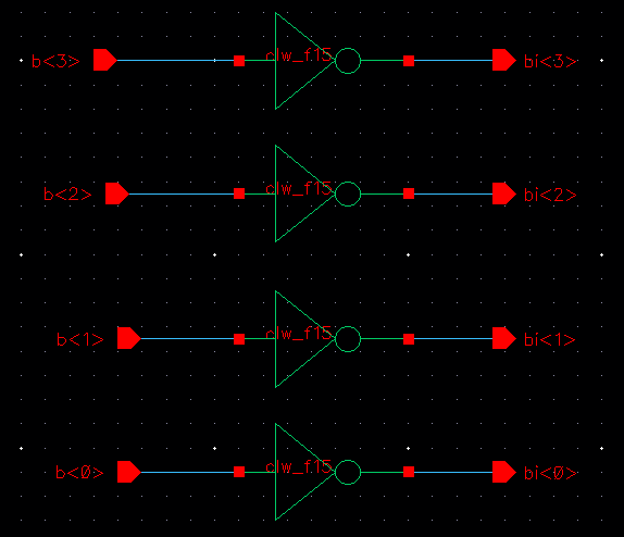
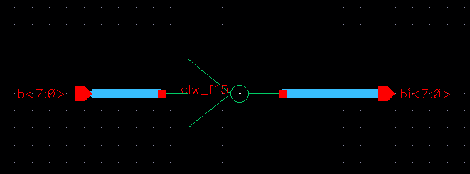
I. 4-bit word Inverter
First step
is creating the 4-bit word inverter using the 6u/0.6u NMOS and PMOS
transistors. Here is my symbol for the inverter that will be used in the schematics, already created in a previous lab....
Below is my schematic. As you can see there is
a single inverter for each input/output (4 inverters total).
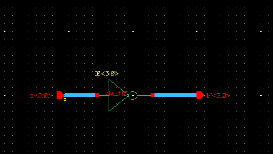
To
create a more compact and clean schematic, we'll utillize buses and
arrays so that we minimize components. Shown below is the
equivalent circuit. The input is named b<3:0> stating that
inputs b3 through b0 are included on the input bus, and just the same
as outputs bi3-bi0 included on the output bus. Editing the
instance name of the inverter to inclue the array of 4 inverters
(<3:0>) as shown below ties each input to the output along
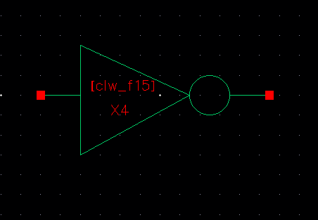
the buses. Also, below is my 4-bit inverter symbol for the
schematic that can be used as a single component in larger circuit
schematics helping compact the design even more.
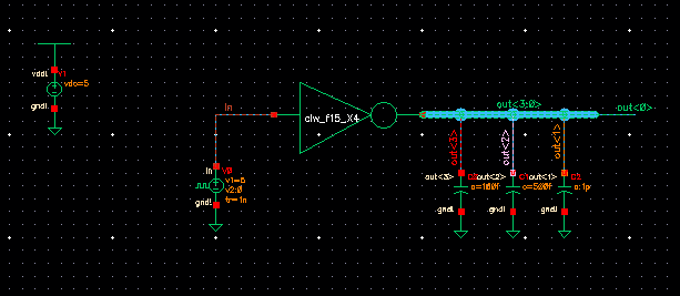
Here
is an example of the 4-bit inverter being used in a simulation circuit.
Here, each output is going to it's own load. Following
below are the simulation results.
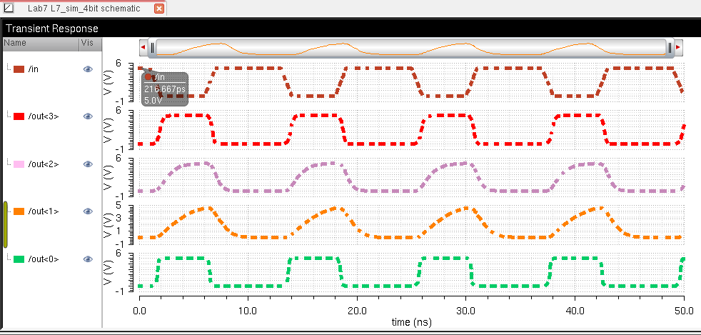
The inverter works as expected... Inverters the input on each output as
you can see. You can see the different effects that the varied
sized capacitors have on the outputs as well. The larger the
capacitor, the longer it takes to charge and discharge when the input
pulse switches. This causes longer delays and slower rise/fall
times of our outputs. This is obvious looking at the simulation
results below. Our<3> has a very tiny capacitive load, and
Out<0> does not have one at all, they have much quicker rise/fall
times and much less delay than the other two with larger capacitive
loads.
Out<3> --> 100fF cap
Out<2> --> 50fF cap
Out<1> --> 1pF cap
Out<0> --> No capacitive load
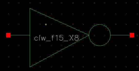
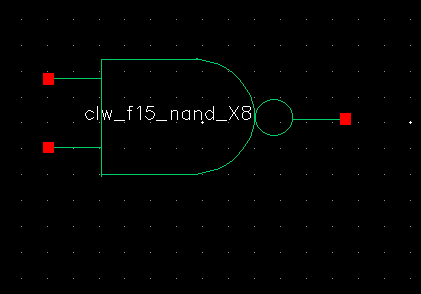
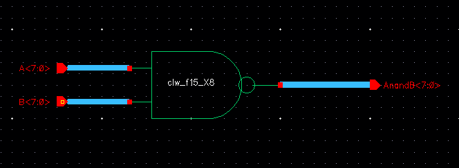
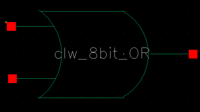
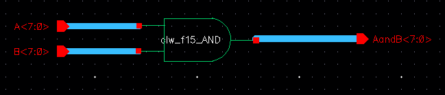
II. 8-Bit Gates
Next for this lab we created schematics and symbols for an 8-bit input/output array of: NAND, NOR, AND, inverter, and OR gates. Also, simulated to show they are working correctly and behave as we expect...
A. Inverter
As already seen before, below is the inverter
symbol and schematic for the 8-bit array. (Please note that simulations
are done all together after each gate is created)
B. NAND Gate Array:
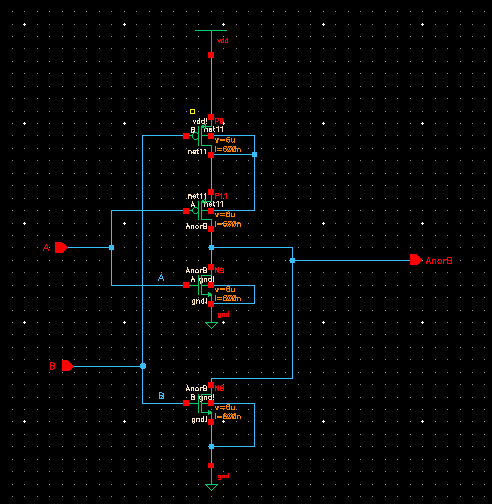
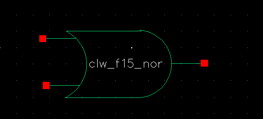
C. NOR Gate:
Below is the symbol and root schematic for the single NOR gate.
We had not yet used this gate before so the base schematic is
shown here.
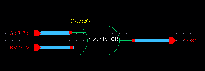
D. OR Gate:
For the OR gate I simply included an inverter on
the output of the NOR gate in the schematic. So below is only showing
the schematic and symbol of the OR array.
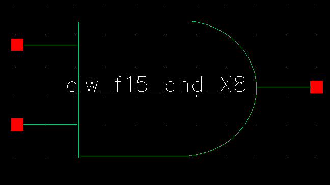
E. AND Gate:
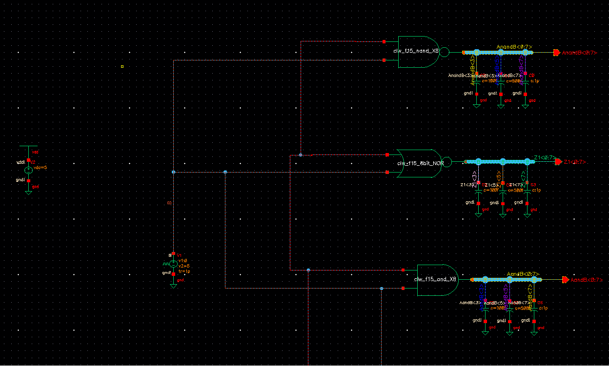
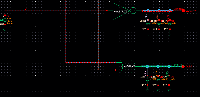
F. SIMULATIONS:
Below is my simulation schematic. So it would be easier to
see it's snap-shotted in two parts (top and bottom), but connected as
one circuit. I used the same three capacitors for load examples,
100fF, 50fF, and 1pF. You can see each arrayed gate with a simple
input and the bused outputs.
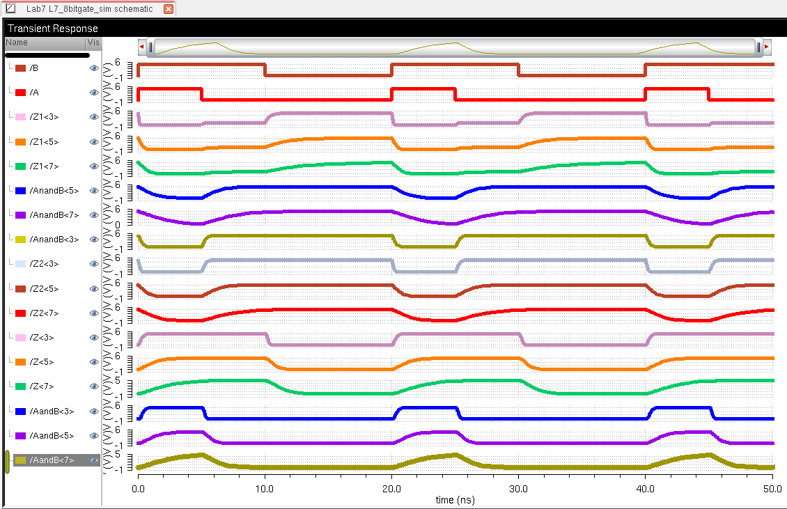
Below are the simulation results: You can see once again with
each gate the output is greatly dictated by the size of the capacitor.
Also, observing the behavior of each gate, the graph shows that
each perform as expected.
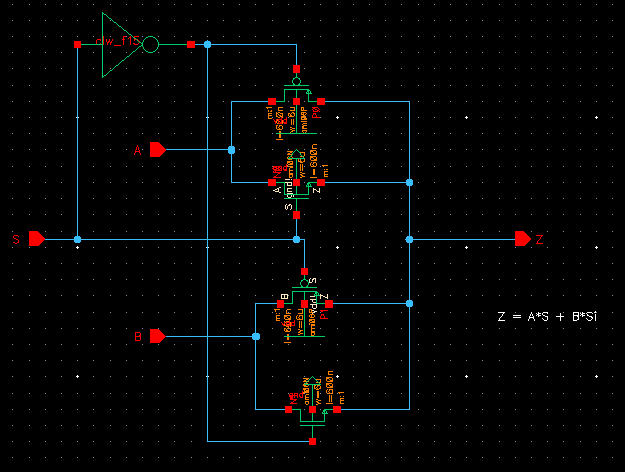
III. MUX/DEMUX
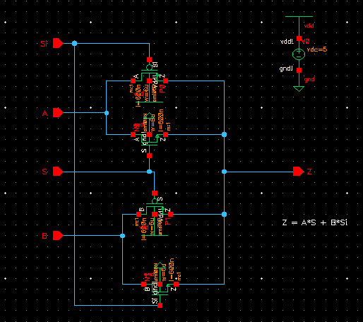
Below
is a schematic of a 2-to-1 DEMUX/MUX (demultiplexor/multiplexor) given
to us in the lab, along with the symbol representing it. So the
way this circuit works is, you have two inputs (A and B), a single
output (Z), and Select (S/Si - inverse select). The expression
was given with the schematic: Z = A*S + B*Si What this is
stating is the if Select =1, then Z =A, but if Select =0 (Si =1), then
Z =B.
Below is an example of a Truth Table for the MUX.
| A | B | S | Si | Z |
| 0 | 0 | 0 | 1 | 0 |
| 0 | 1 | 0 | 1 | 1 |
| 1 | 0 | 1 | 0 | 1 |
| 1 | 1 | 1 | 0 | 1 |
You
can see that when S is high (logic 1), the Z = A. And when Si
is high (Si = 1 and S must be 0) then Z = B. Basically, in
very simple terms, your S (select) selects which input you will
transmit to the output, either A or B in this case.
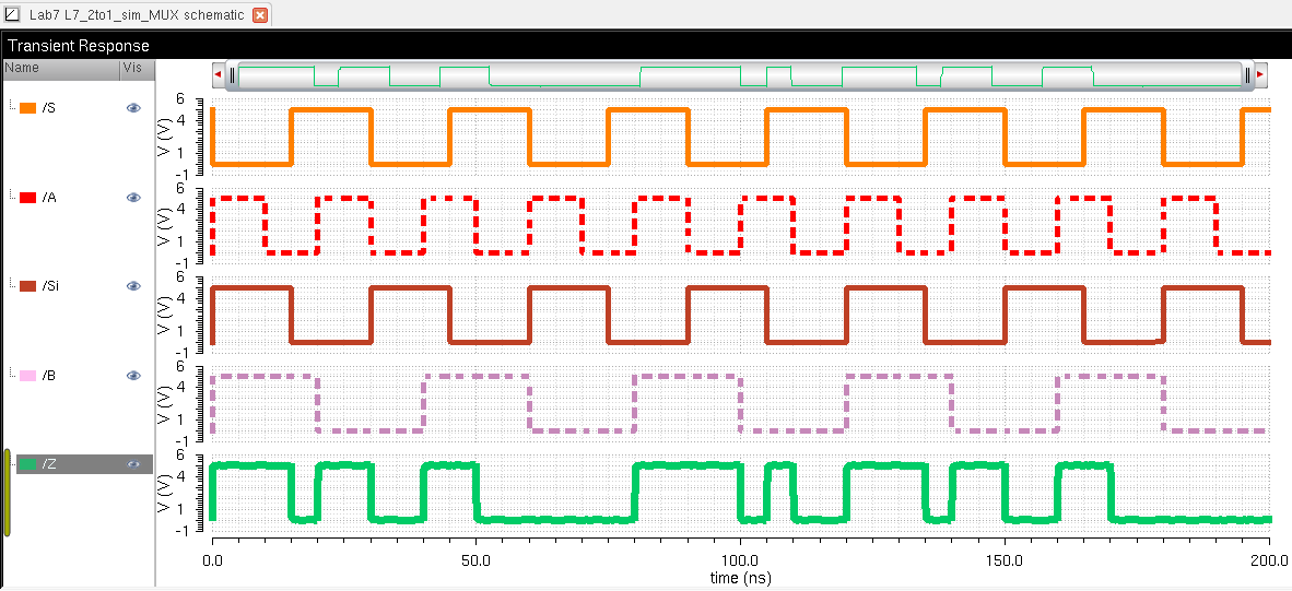
Next, I constructed the following schematic in order to show how the MUX/DEMUX behaves through simultations.
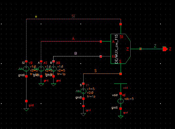
As you can see, the S and Si are inverses of each other.... Looking
down at the Z output it is very easy to visualize which input (A or B)
is being selected. Once again, As S goes high, Z = A, and As Si goes
high, Z = B.
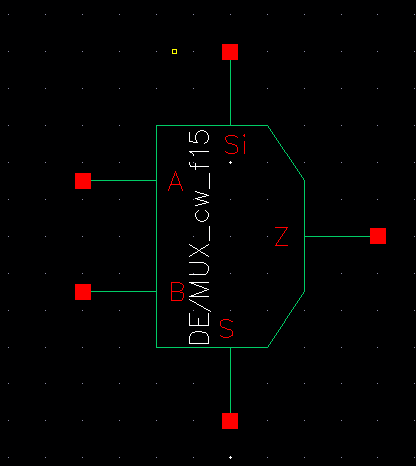
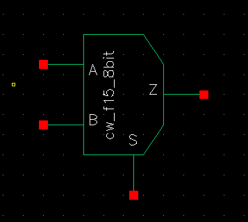
Next, we use an inverter connected to the S input to eliminate our Si
input. This will help us have one less connection to worry about
when using our MUX symbol in larger circuit schematics in the
future.... Below is the newly renovated circuitry.
Below is our new symbol (8-bit symbol shown and is an exact
replica of the symbol created for the base schematic, which was
instantiated in the schematic below) with one less limb and our 8-bit
MUX array schematic.
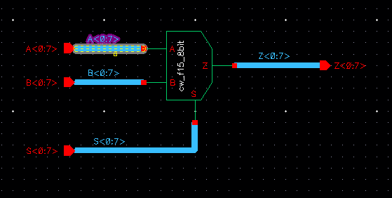
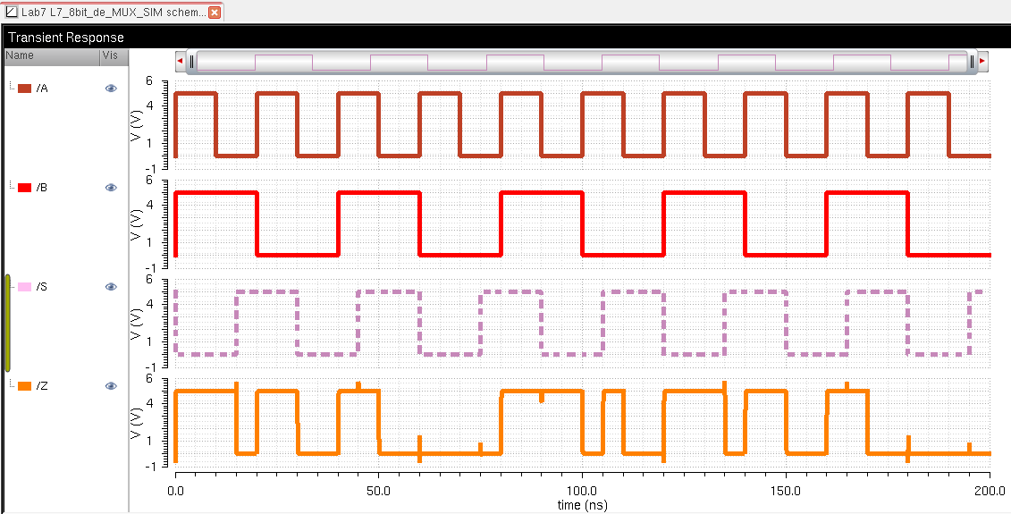
Simulating our 8-bit MUX, we see the results are still the same as the logic has not changed.
IV. Full ADDER
Now we draft the schematic of the full-adder seen in Fig. 12.20 of the CMOS textbook using 6u/0.6u devices (both PMOS and NMOS).
A. Full Adder
Below is my schematic...
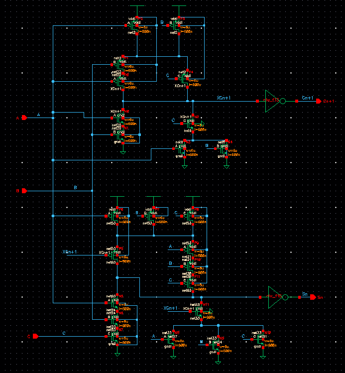
After constructing the above schematic, I created a symbol to use
to represent it in other schematics. Below in the circuit you can
see the ADDER symbol.
B. 8-bit ADDER
Here you can see that with using buses and arrays as in previous
8-bit gate construction, I have created a schematic of an 8-bit ADDER.
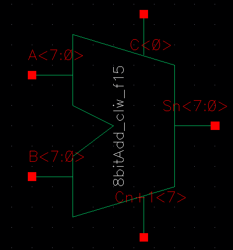
Next, following this circuit you will see the 8-bit ADDER symbol
in which it is encompassed.
Using similar bus labeling as in Tutorial 5's explanation of a ring oscillator, I was able to ensure that carry OUT of one ADDER went to the carry IN of the following ADDER...
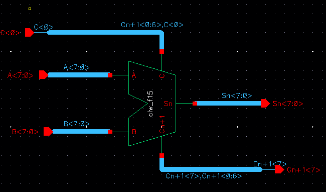
Below is my simulation schematic that will be ran to verify performance of the 8-bit ADDER.
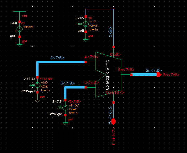
Using similar bus labeling as in Tutorial 5's explanation of a ring oscillator, I was able to ensure that carry OUT of one ADDER went to the carry IN of the following ADDER...
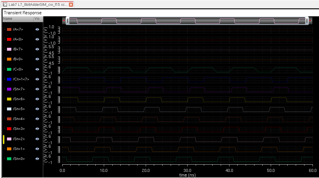
Now after seeing that the schematic of the Full Adder works as
expected, it's time to do the layout... Below you can see the full
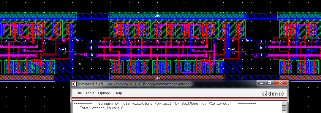
adder with a successful DRC showing no errors.
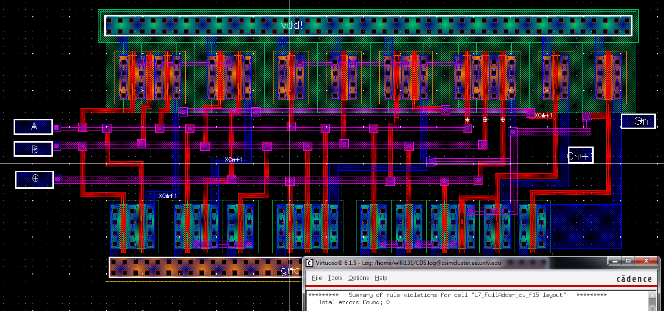
Next extracting the layout (shown below), you can see all the connections clearly.
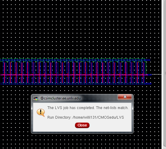
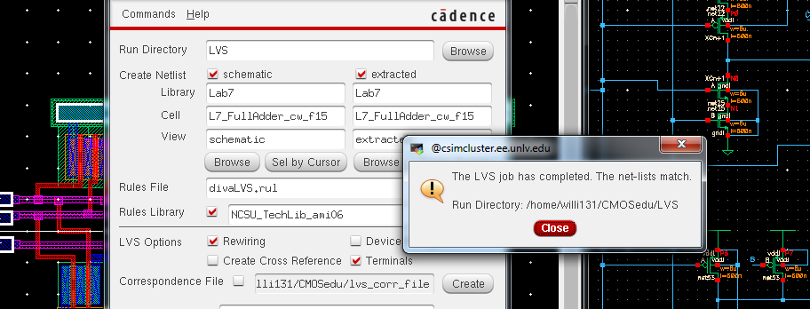
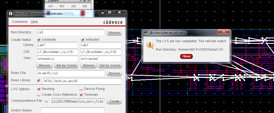
From
here we run an LVS check and you can see that it was ran successfully
with netlists from the extracted layout matching the schematic of the
full adder.
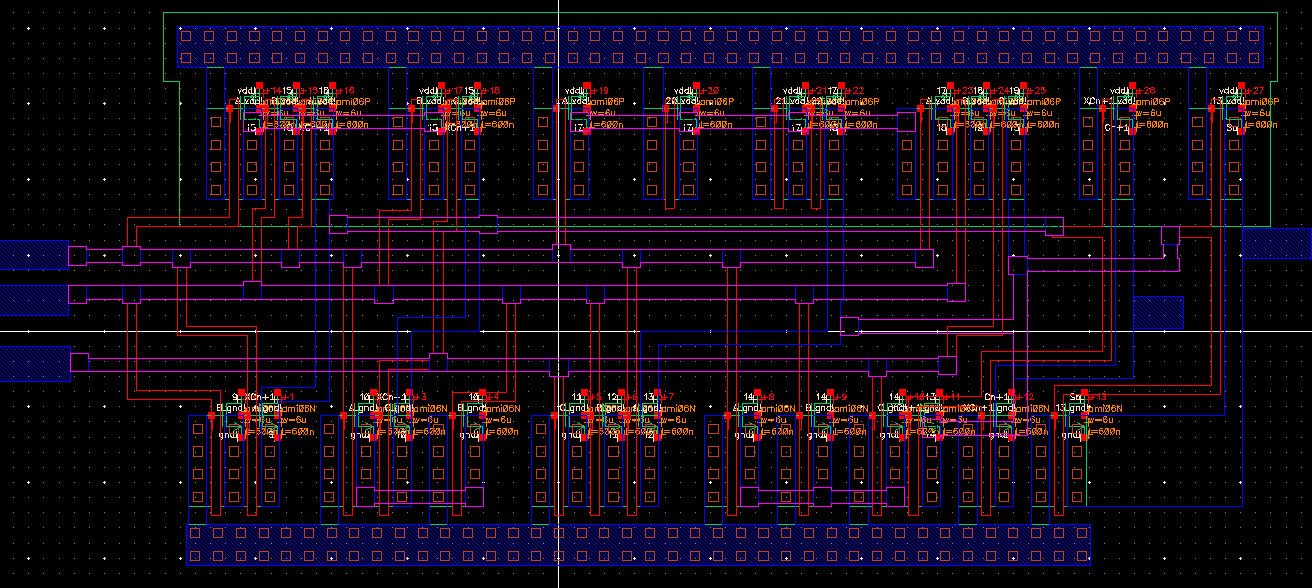
Next, Laying
out the 8-bit adder is less than a challenge since we already have the
matching netlists from a single bit adder.... By instantiating the
layout 8 times and connecting each Cn+1 (Cout) to the next C (input) of
the following cell an 8-bit adder is constructed. Below you can
see an example of the connections and the cleaen DRC ran.
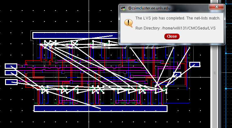
Finally, LVS-ing the extracted 8-bit layout with the schematic we see that netlists match successfully.
Now
after completing this lab we have all the basic building blocks to
construct an ALU that will be done in a lab project to follow. :)
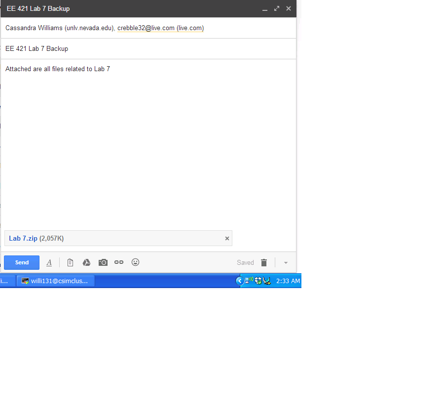
All files related to performing this lab were backed up via email and flashdrive....
Return to Student Lab Reports here.
Return to EE 421L Course page here.