Lab 4 - ECE 421L
Cassandra Williams
Willi131@unlv.nevada.edu
September 21, 2015
PRELAB:
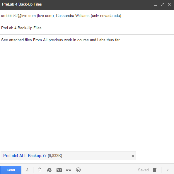
-First, Back-up all of your work from the lab and the course.
-Read through this lab before starting it.
-Go through Tutorial 2 seen here.
-In
the simulations in this lab the body of all NMOS devices (the
substrate) should be at ground (gnd!) and the -body of all PMOS devices
(the n-well) should be at a vdd! of 5V.
I. Back-up for Prelab 4 files and all course work is shown below:
II. Tutorial 2 takes you through step-by-step the Layout and Simulating the I-V curves of both NMOS and PMOS devices.
A. NMOS
- First
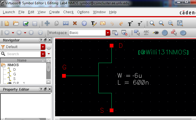
this lab begins simply instantiating an nmos device in the schematic
editor. We connected pins to each the drain, source, and gate.
From there we created a symbol shown below.
-Next,
we built a schematic using the symbol above. After checking and
saving with no errors we initiated the ADE L in order to simulate our
NMOS circuit.
-Once
the ADE opened we had to pull our spectre from the Model Library
ami06N.m. This is found in the ncsu-cdk-1.6.0.beta file set up in
the very beginning of the semester when doing Tutorial 1.
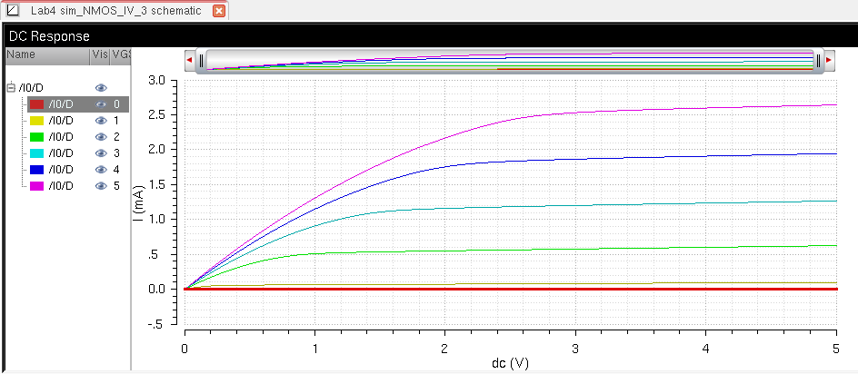
-Once our analysis parameters are all set up, we run a DC sweep... Below is our simulation results.
-So
I will note here that the first half of this tutorial was done for a
homework assignment previously. Therefore the mistakes of
attempting to layout and LVS a 3-lead nmos device rather than the
4-lead device used in the library we pull our nmos component from is
not shown here.
-Next, I created the layout shown below.
a. First I inserted from the NCSU_TechLib_ami06 library an nmos device with the width 6um and length 600nm.
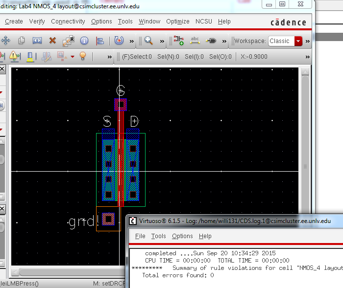
b. Then in order to ground our p-substrate we insert a ptap cell.
This is the box labeled gnd! below. The ptap is the metal1
connection to p+..
c. The simple layout was DRC-ed and returned with no errors.
d. Next, Pins created from metal1 were created and labeled G(gate), S(source), D(drain), and gnd!(p-sub)
e. The DRC ran with no errors and is shown below.
-After
completing a successful DRC with no errors, I extracted the layout in
order to run my LVS. Below is the extracted view of my layout
with a successful LVS ran with no errors.
B. PMOS device Layout and Simulation:
-Here
we essentially repeated the NMOS process (without stumbling through
everything... This time was very quick and efficient design process).
a. First, created a basic schematic using the pmos4 device shown below.
b. After checking and saving with no errors, a symbol was created for later use.
c. Next, we created a Layout of the PMOS device. Notice this time
our ntap is connecting our B (body) to what will be VDD!.
d. The layout is DRC-ed succesfully with no errors as shown below.
e. After we know the layout is good and has no errors we extract it as shown below.
f. Finally we construct the circuit below. So if you pay
close attention you may notice that I have made a mistake... After
trying to run my simulation from the extracted layout I figured out my
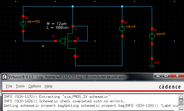
error in labeling.... Because this is a pmos, my V0 is VSG, NOT VGS!
This is stressed in the tutorial and was corrected in my circuit
in order to get successful a LVS. (You can see this correction in the
LVS netlist below!)
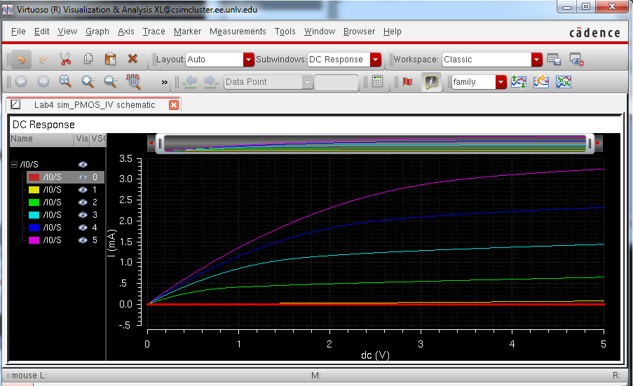
g. Below is my simulation results, DC Sweep again...
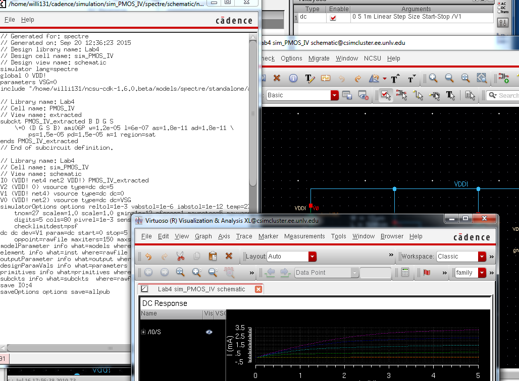
h. Lastly, editting my environment options in the ADE, I state to
run the extracted layout... Below shows the simulation results (same as
the circuit simulation) as well as the Netlist.
- You can see in the 2nd paragraph of the netlist that this is ran from the EXTRACTED view.
POST LAB REPORT:
September 28, 2015
In
this lab we generated 4 schematics and simulations illustrating IV
curves for NMOS and PMOS devices. Then we created each an NMOS
and PMOS layout with connections to probe pads.
1. NMOS
A. ID vs. VDS
Below is the circuit I used for my NMOS device. This was generated through tutorial 2 and the prelab.
You can see that we have voltage
sources on the VGS and VDS terminals. Also, our Source and body
are grounded. (The body being grounded is a standard for NMOS
devices)
After checking and saving without errors, I launched the ADE L
in order to simulate my circuit. Below shows my simulation and
parameter settings. Here I ran a DC sweep. VGS was varied
from 0V to 5V in 1 second steps and VDS was swept from 0V to 5V in 1 ms
steps. As you can see, the output selected was for Node N0/D.
(This is the current, ID)
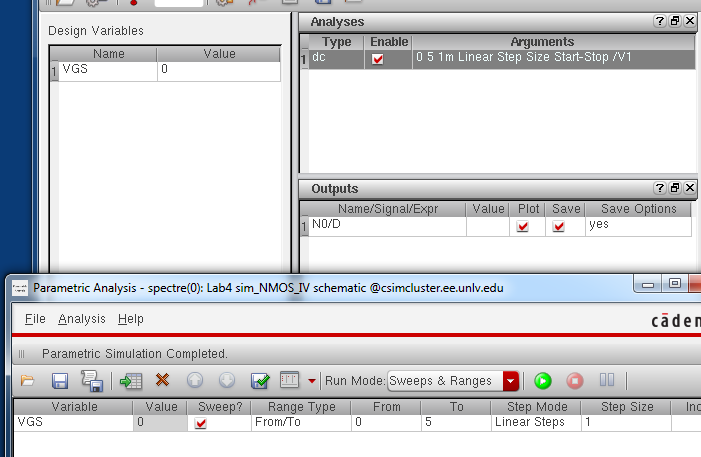
*As a side note, if VGS was left at 0V
rather than turning on to 5V as show above, there would be no current
flow through the MOSFET.*
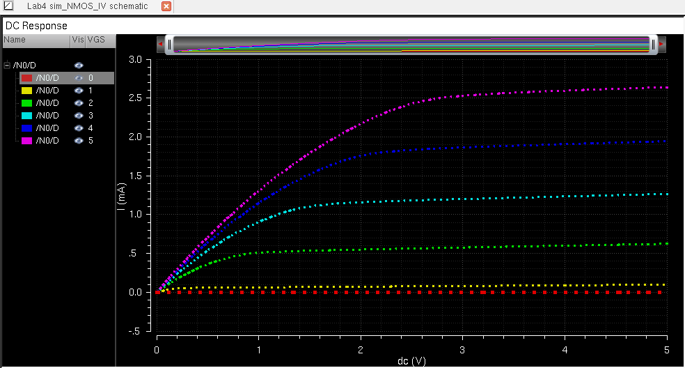
Below is my output. You can see each curve for the corresponding voltage step in voltage.
B. ID vs VGS:
Below shows the schematic for our next
simulation. Here you can see that this time VDS is held to 100mV.
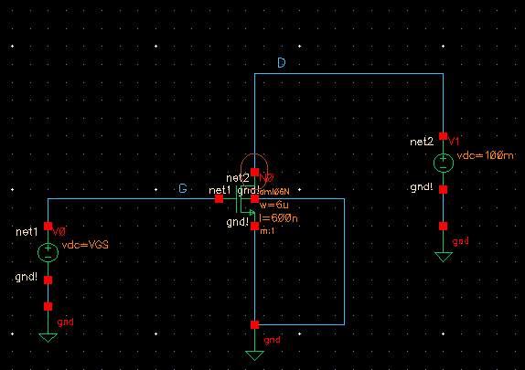
This time we will hold VDS constant and
perform a DC sweep on VGS with VGS varying from 0V to 2V as seen below
in the simulation parameters.
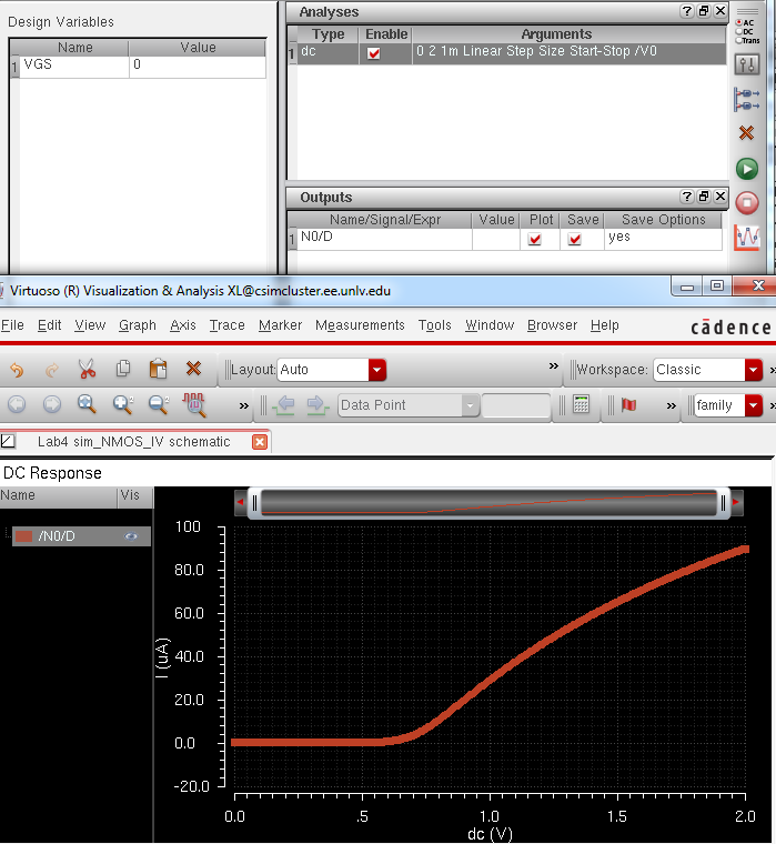
Above shows our simulation results.
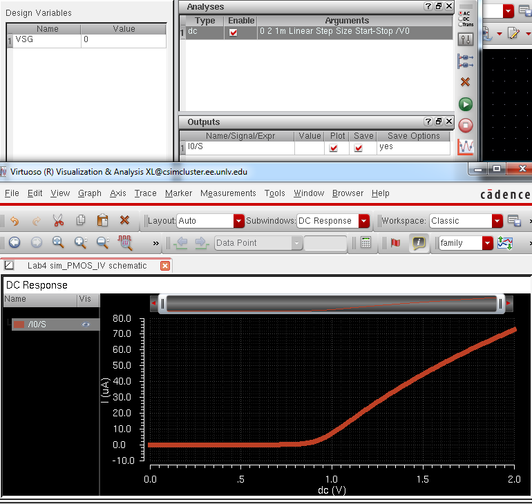
2. PMOS
A. ID vs. VSD
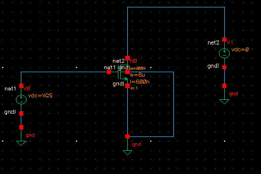
Next, I constructed the schematic to use for my PMOS device simulations.
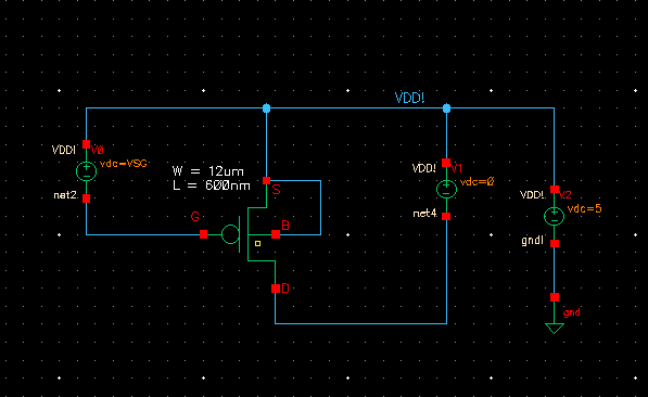
For this schematic, you can see that our
Body of the PMOS is connected to VDD, opposed to Ground like the NMOS.
Also, our Drain and Source are inverted. Below shows the
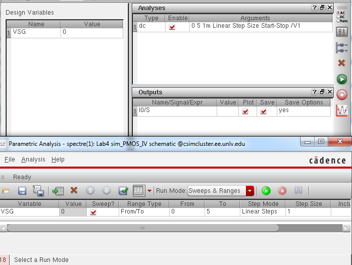
simulation parameters used. You can see that we run VSG
from 0V to 5V in 1 s steps and sweep our VSD as it varies from 0V to 5V
in 1ms intervals.
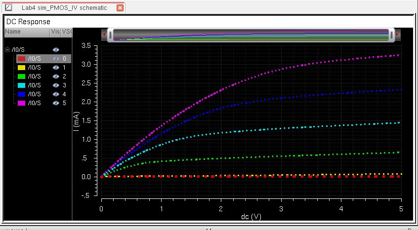
Below is my simulation results.
You'll notice they are VERY similar to my first NMOS simulation
IV curves.
B. ID vs VSG
For our second simulation I used the
schematic below... Here you can see that VSD is set to 100mV.
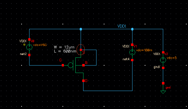
The parameters for the simulation are set
to sweep VSG as shown below. You can see that our IV curve from
our simulation output is very similar to the one of our VGS sweep done
for the NMOS device.
C. Layouts with Probe Pads
1. NMOS
First, a schematic was created for the Probe
Pad by simply instantiating a pin with a single lead. As shown
below, after this was created I then developed a layout of the Probe
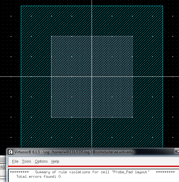
Pad in order to use in the NMOS/PMOS layouts. The Probe Pads are
simply layed out using a layer of metal3 and glass. This was made
according to C5 processing rules (Significantly smaller than our Bond Pads created in previous labs)
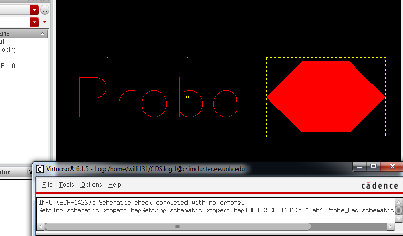
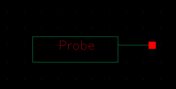
The symbol below was created to utilize in my schematic for my device-pad connections.
Next, I created a schematic with an NMOS device.
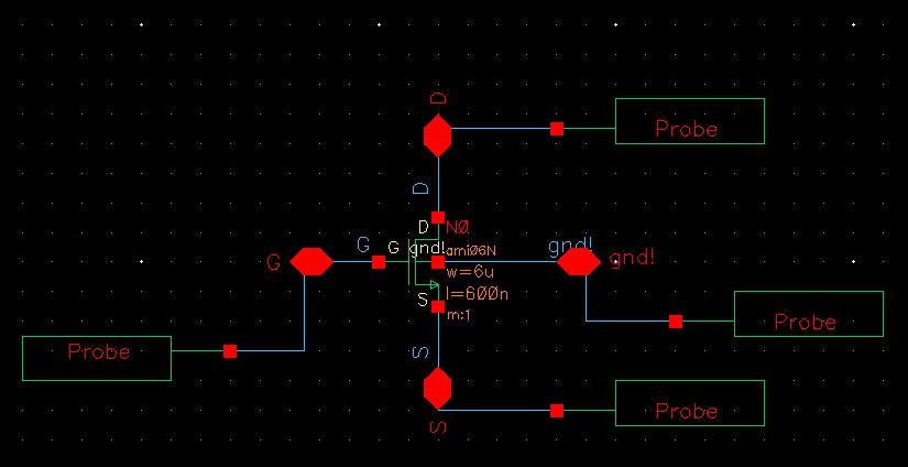
After checking and saving my schematic
successfully without error, I created a layout of my NMOS device. (nmos
chosen from the ami06 library) Below you can see that connections
to the NMOS are made using metal1. Then a path is created to a
connection layered with m2_m1 and m3_m2 in order to continue my
connection path (then on with metal3) to the probe pads.
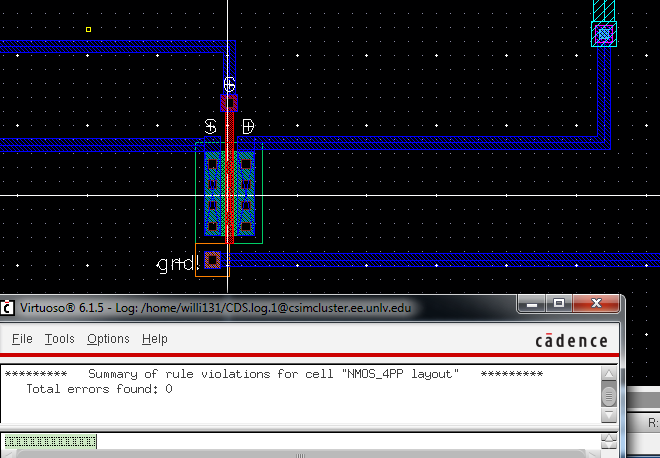
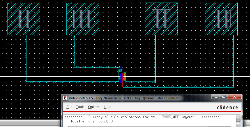
DRC was ran with no design rule violations.
Below is another view of the layout, zoomed out including the
probe pads. You can see that the NMOS device is still
significantly smaller that the probe pads, even as the probe pads are
still significantly smaller than bond pads....
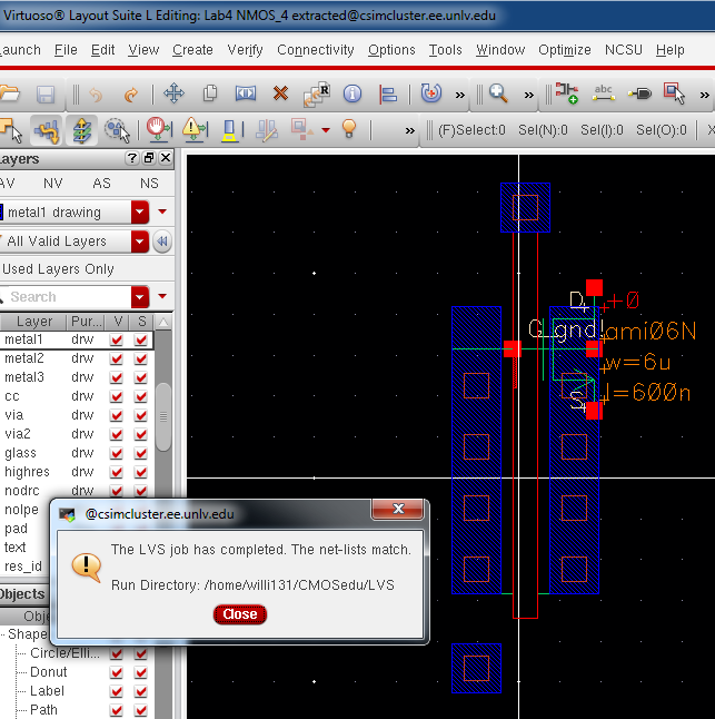
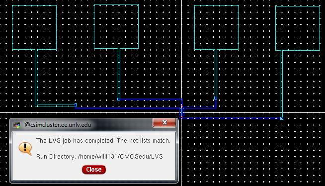
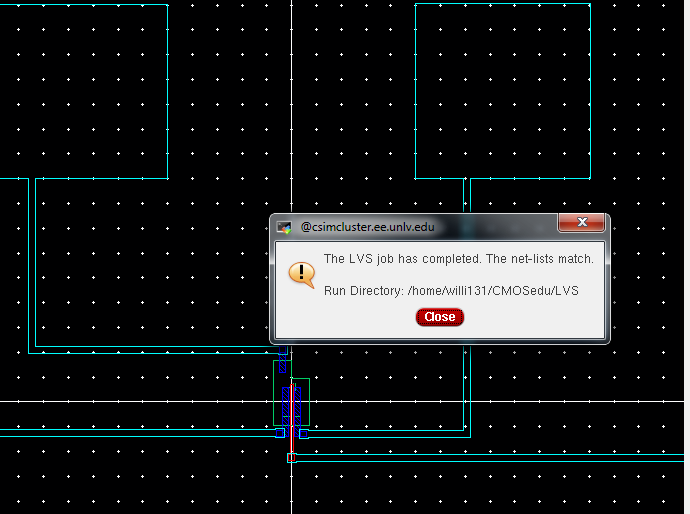
Next, I extracted my layout and ran an LVS
with the schematic shown above. As you can see below, LVS was
successful.
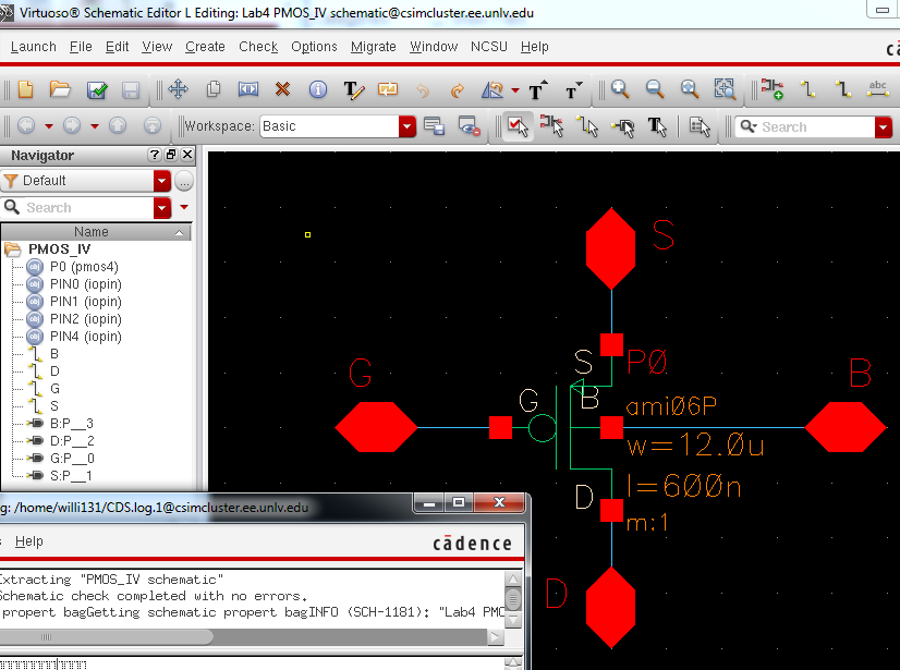
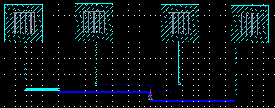
2. PMOS
Next, I repeated steps above rather this
time instantiating a PMOS device from the ami06 library (pmos).
Below shows a good view of the MOSFET.
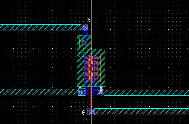
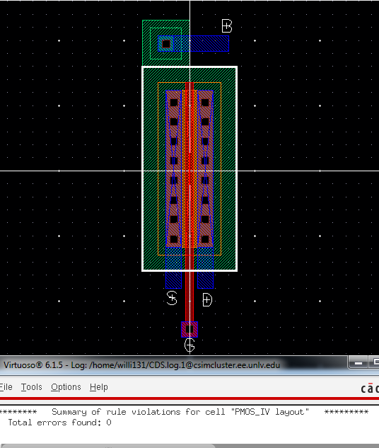
PMOS layout DRC returned with no errors...
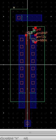
Next, I extracted my PMOS layout and ran a
successful LVS. (The schematic for the PMOS was created just as the
NMOS schematic with pins and probe pad symbols)
Files and clips for this lab were all backed up by email and flash drive.
Return to Fall 2015 421L Here.
Return to Student Lab Reports